Lab 6 - ECE 421L Fall 2023
Pre-lab:
The prelab wants us to go through Tutorial 4.
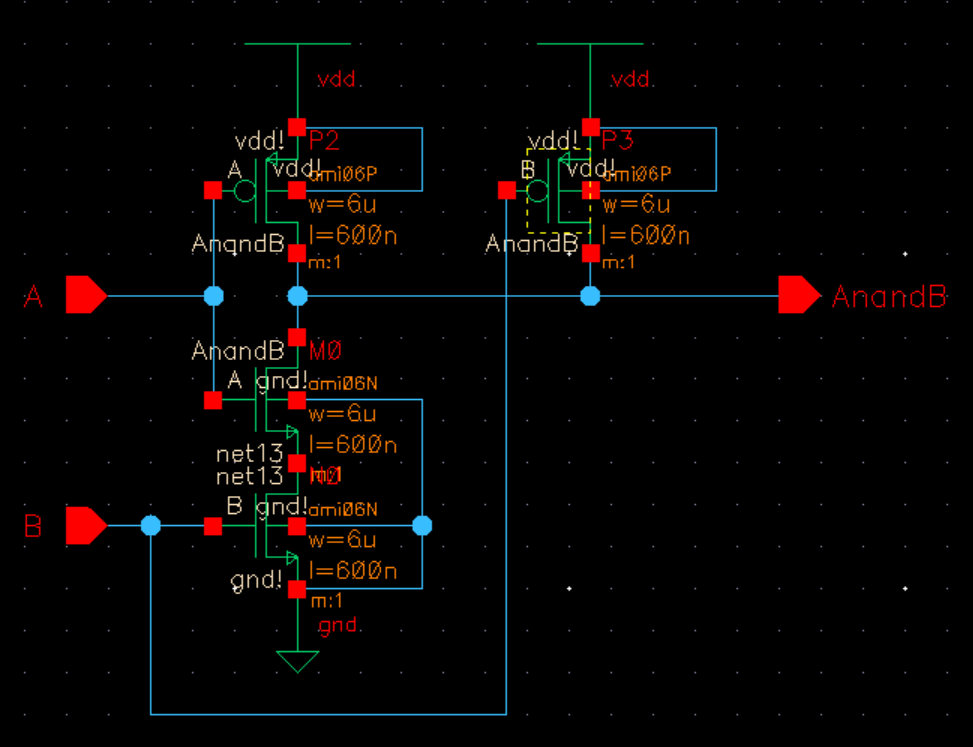
First we will create a schematic for our NAND gate.
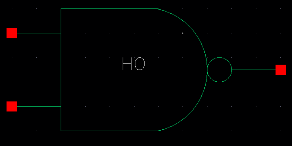
Next we will create the symbol for our NAND gate.
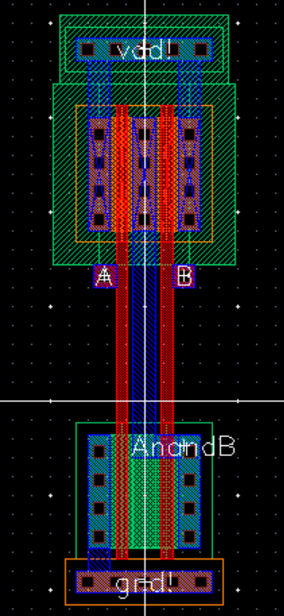
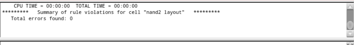
Next, we will create a layout for our NAND gate, and DRC check it,
Now we will extract the layout and LVS it.
The next thing to do is make a schematic for simulating the NAND gate, and then simulating it.
Lab:
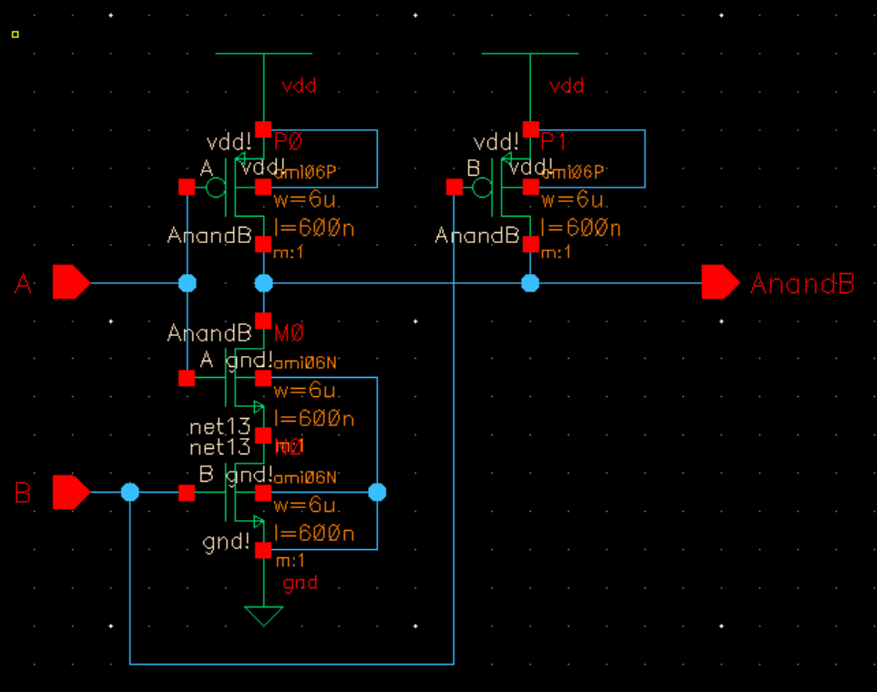
We are going make a schematic, layout, and symbols for a two input NAND gate that is 6u/600nm.
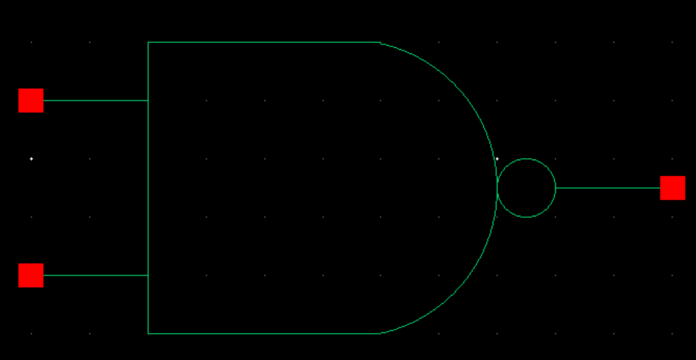
First, create a schematic of the 6u/600nm 2-input NAND gate, then create a symbol for the NAND gate.
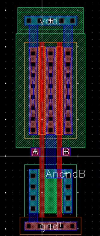
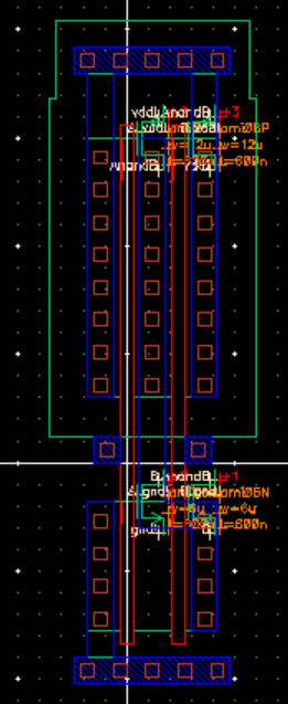
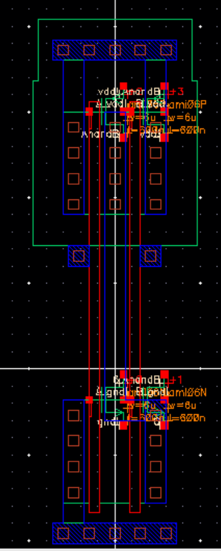
Next, create a layout of the 2-input NAND gate.
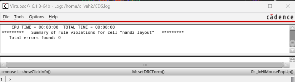
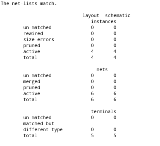
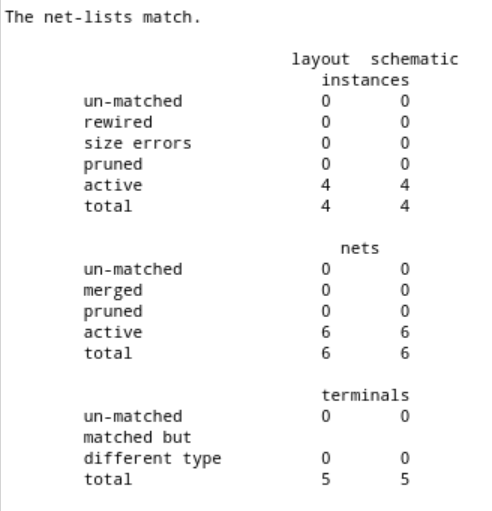
Next, we will DRC the 6u/600nm NAND gate, and then extract the layout and LVS it.
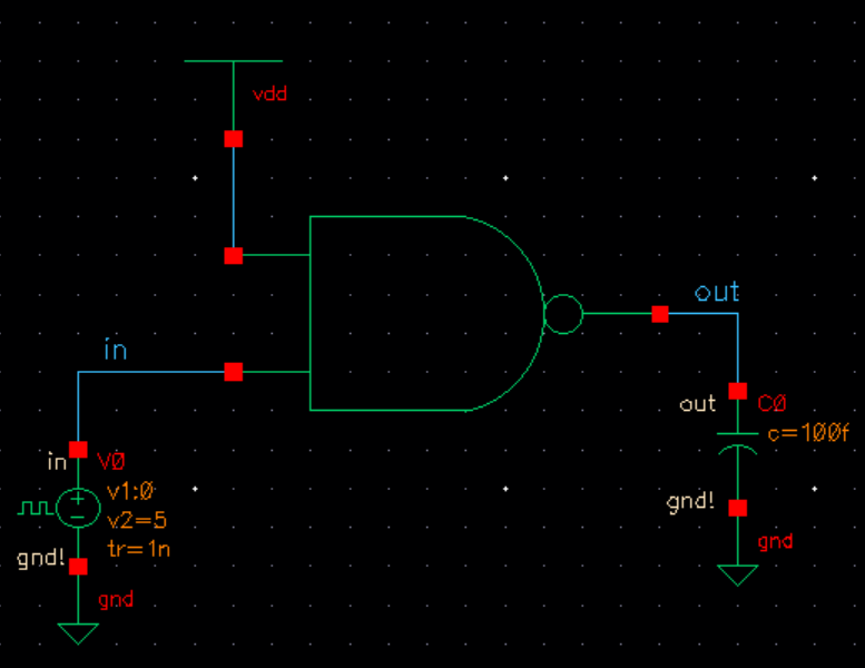
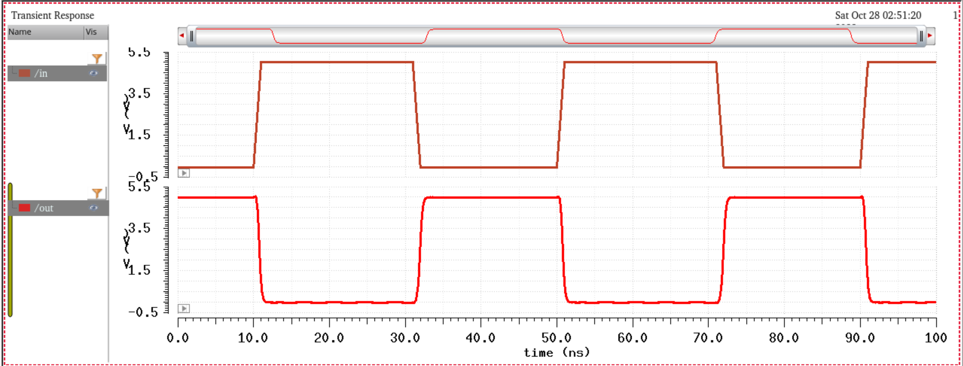
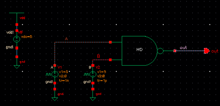
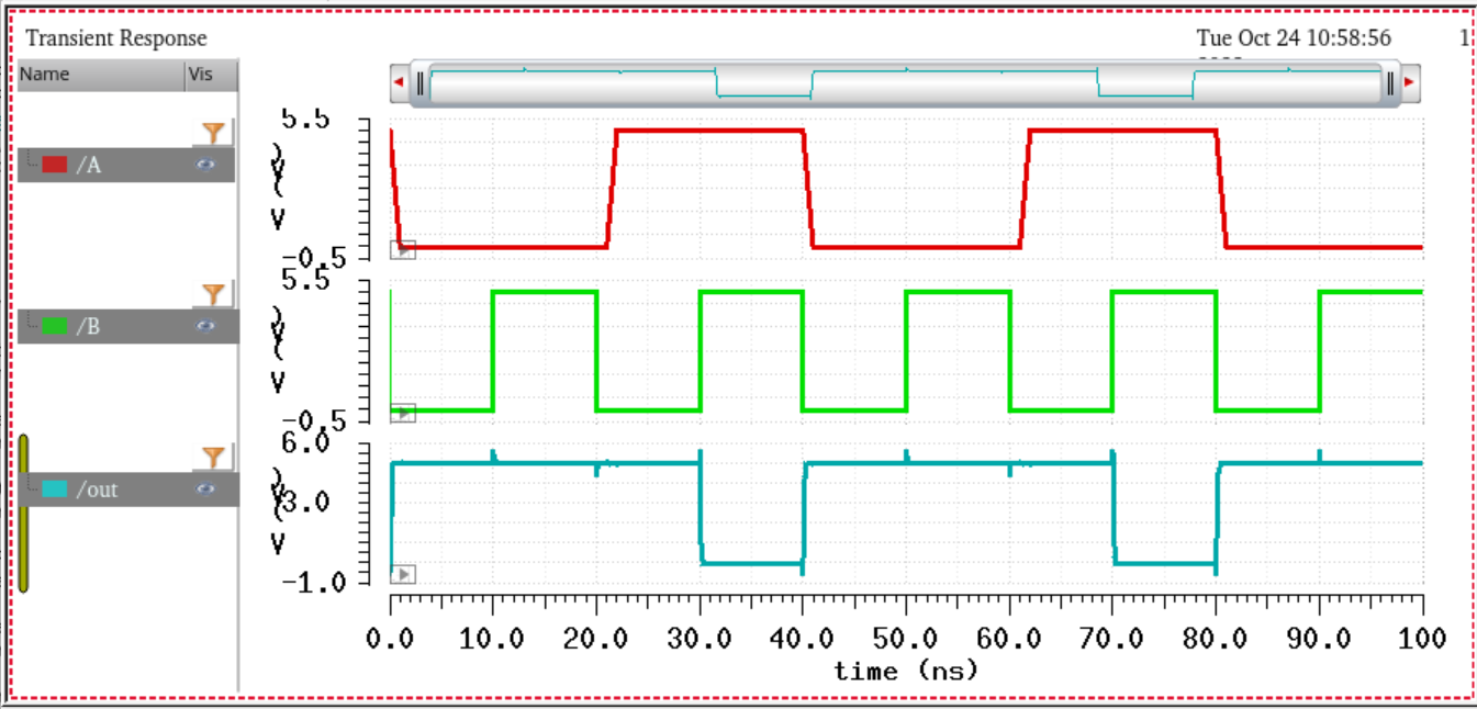
Next, we will create a circuit for simluating the NAND gate.
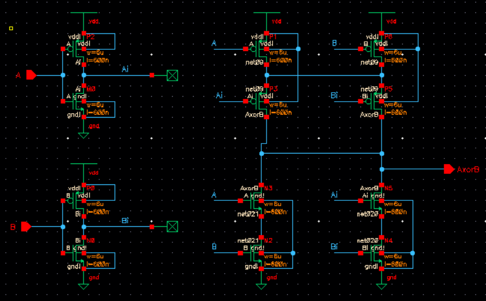
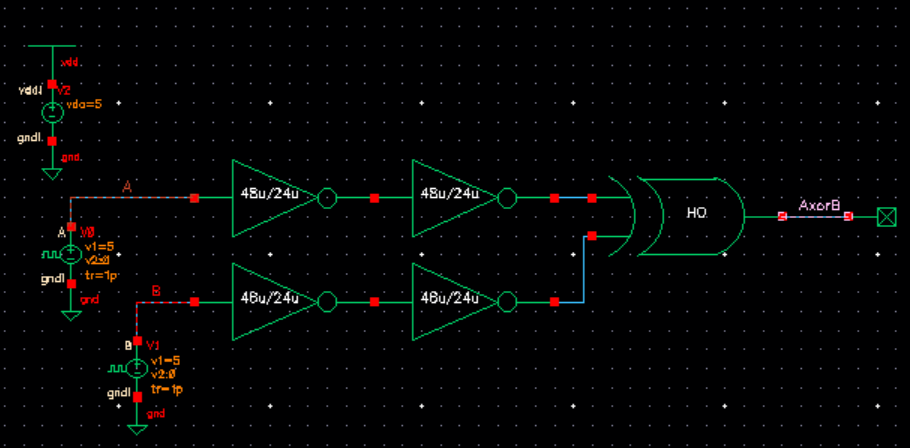
The next part of the lab is to create a schematic for a XOR gate. The first thing we will make is the schematic.
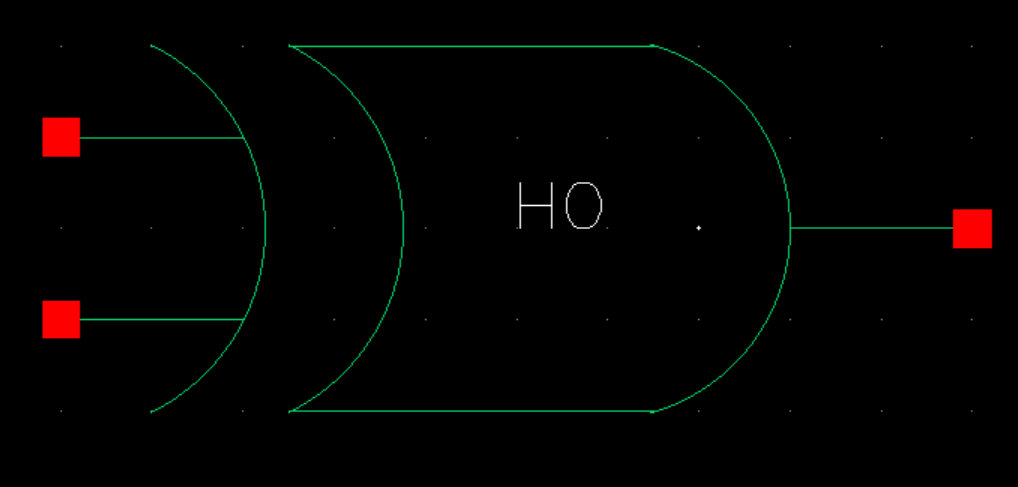
The next step is to create the symbol for the XOR gate.
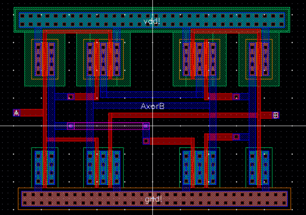
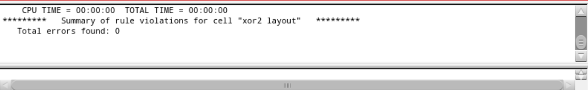
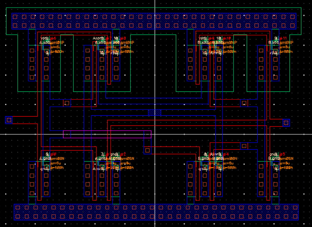
Next, we will create a layout for the XOR gate and DRC check it.
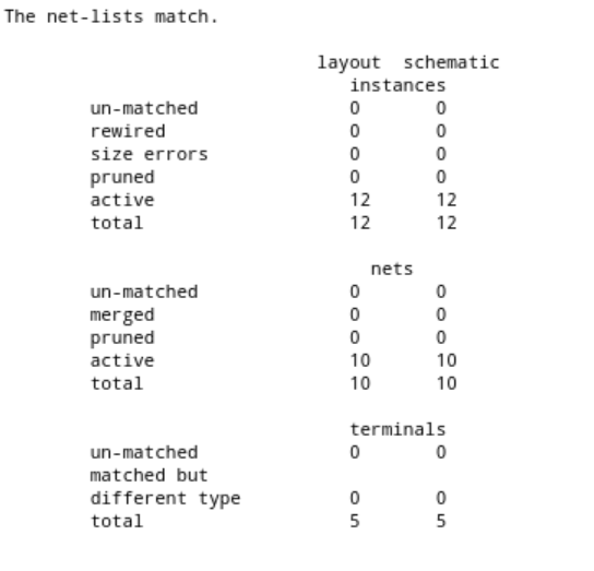
The next step will be to extract the layout and LVS it.
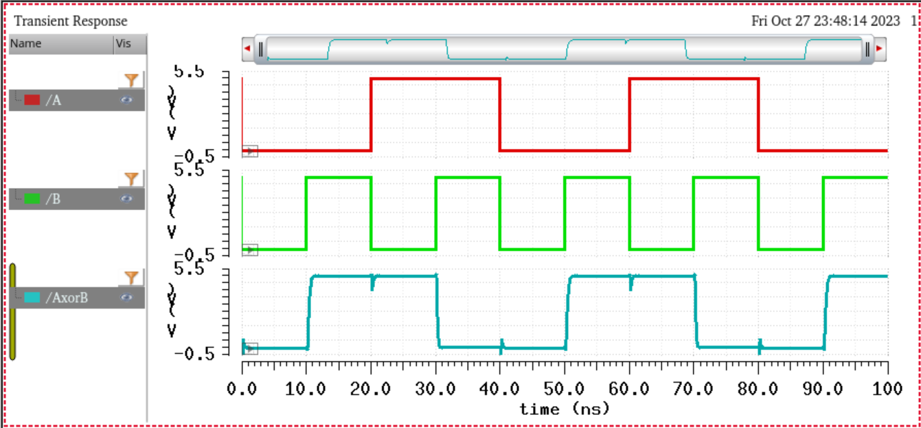
Following LVS completeing, we will make a circuit for the XOR gate and verify its outputs.
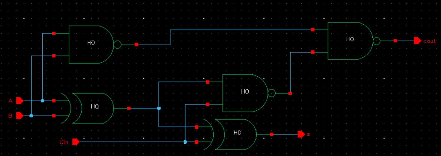
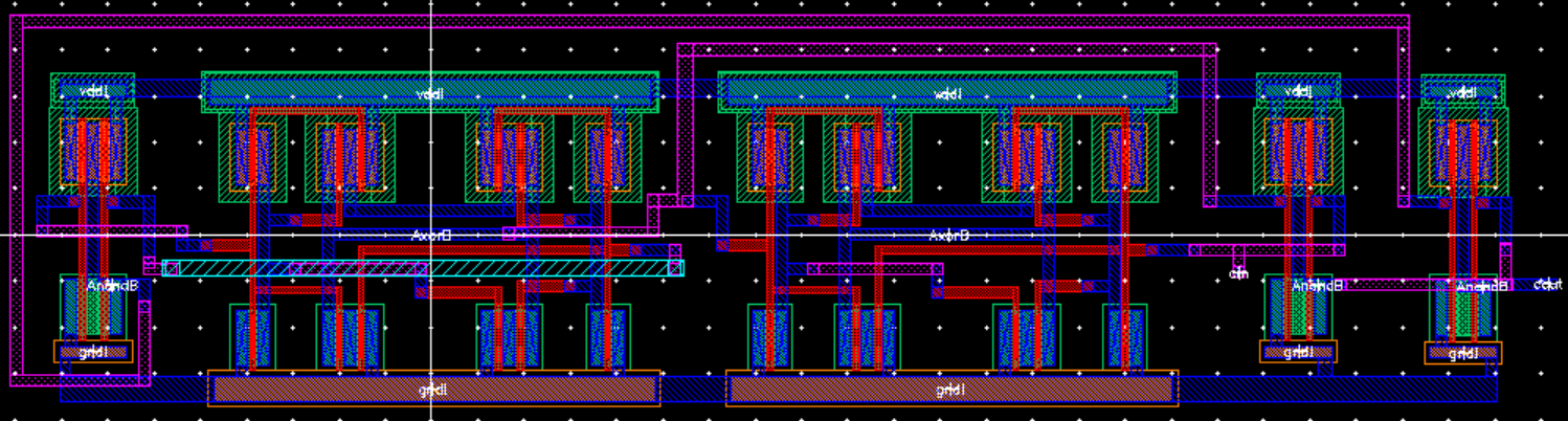
The next thing to make within this lab is a Full-Adder. The first step is to use the symbols that we created earlier in this lab
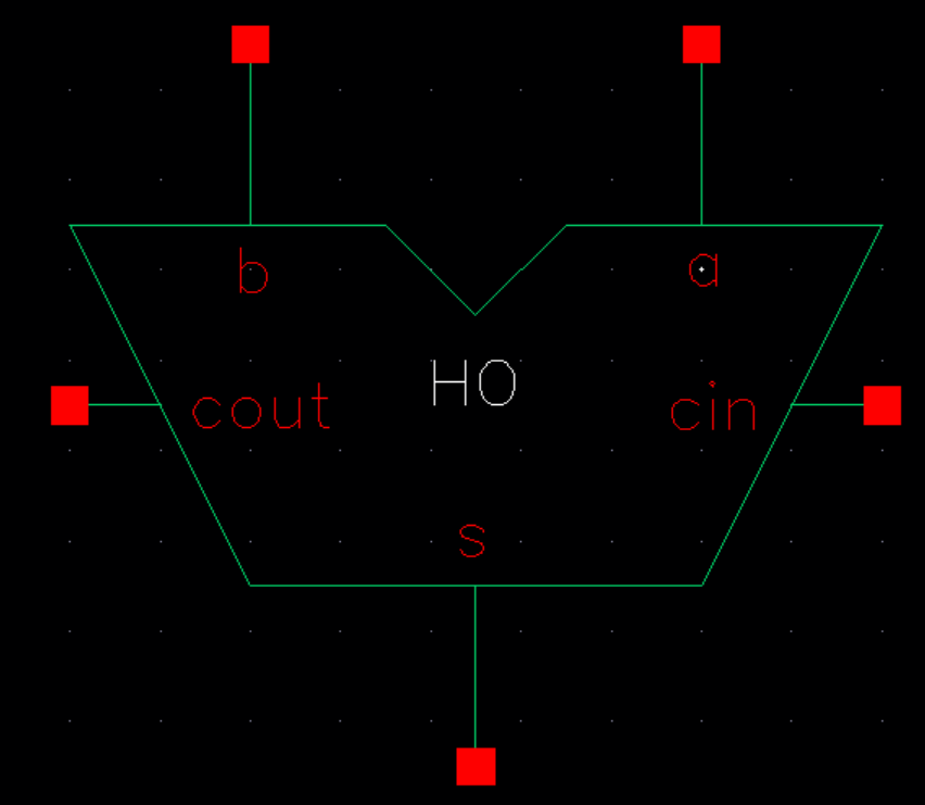
to make the schematic for the Full-Adder. Then following the schematic we will create the symbol for our Full-Adder.
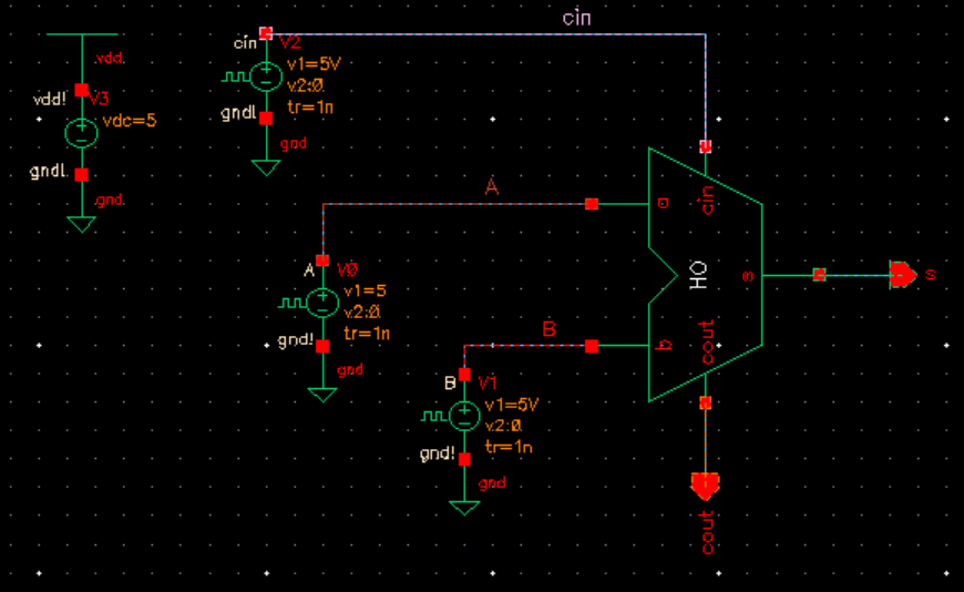
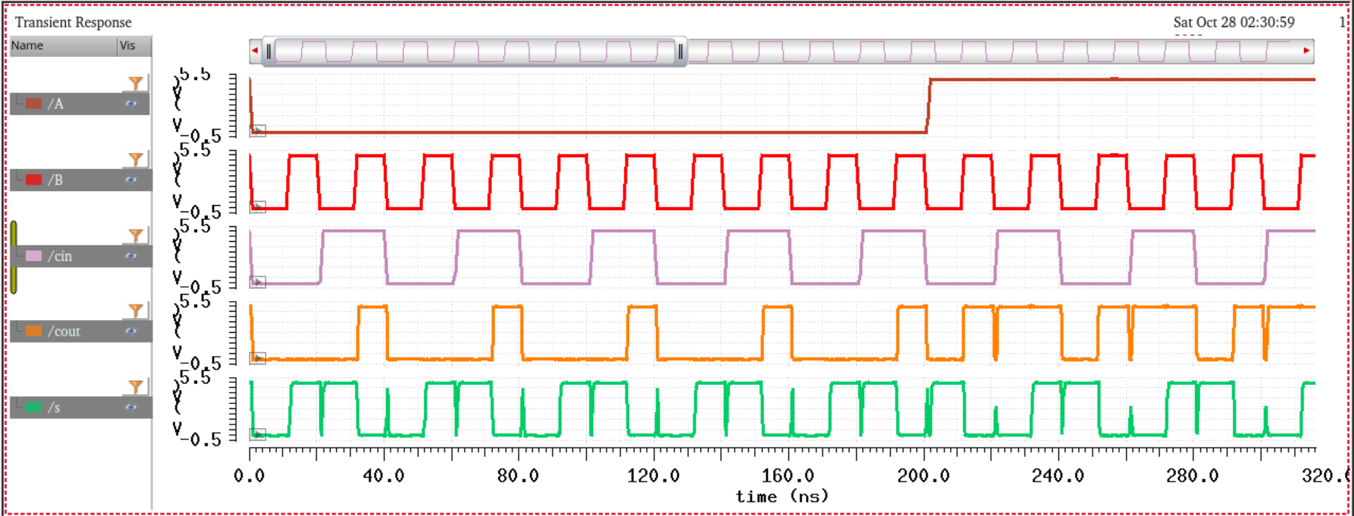
The next step will be to create a circuit for the Full-Adder and checking its outputs, by simulating it. Then to create a layout of
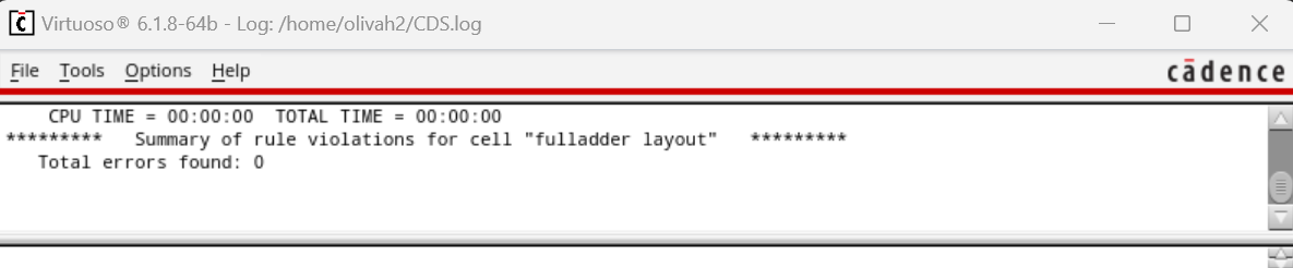
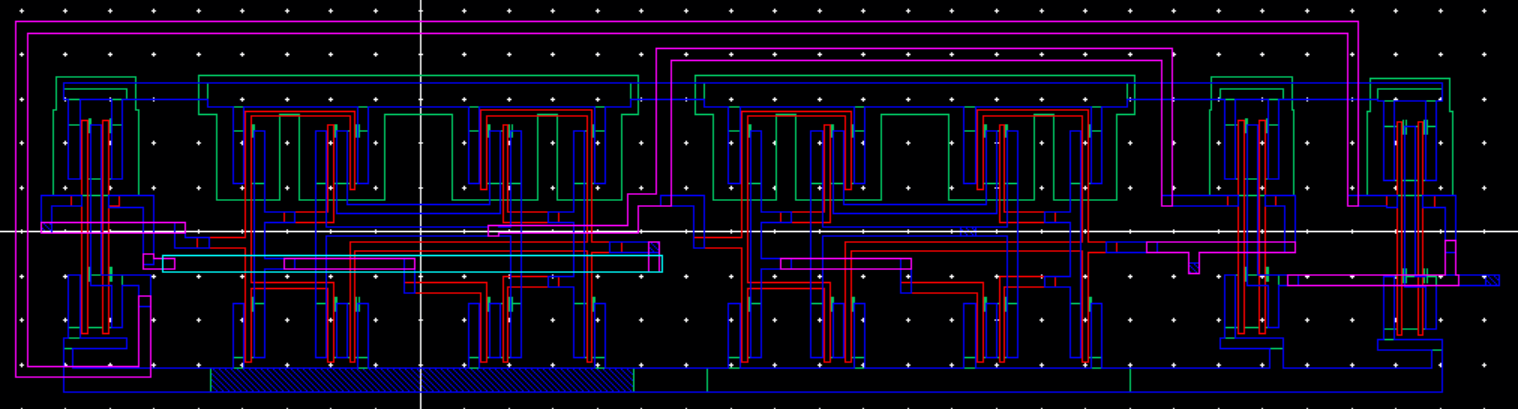
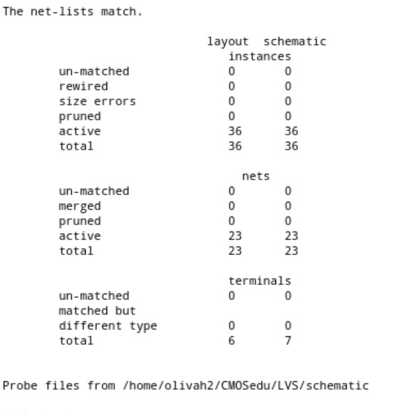
the Full-Adder checking that it DRC. Then extract the layout and LVS it making sure it does match.
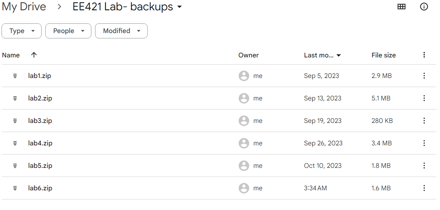
Back-up Files
Return to EE 421L Labs