Lab 5 - ECE 421L Fall 2023
Pre-lab:
We are to go through Tutorial 3 of the pre-lab.
Tutorial 3 begins with questions to answer:
1) What does the Bindkey q do?
- q is to edit object properties
2) Which two Cell Views are used when doing an LVS?
- The schematic and extracted cell views are used
3) What is the difference between the nmose and nmos4 schematic cells?
- The nmos has only 3 connections (Gate, Drain, Source), while nmos4 has 4 connections (Gate, Drain, Source, and Body).
4) How do you select the MOSFET models in the ADE window? What does ADE stand for?
- To select the MOSFET models launch ADE -> Setup -> Model Libraries and follow the path
/$Home/ncsu-cdk-1.6.0.beta/models/spectre/standalone then select nmos (ami06N.m) or pmos (ami06.P.m)
5) What is the difference between moving and stretching?
- Moving is when you move the entire object you selected, while stretching changes the size of your object's dimensions.
6) How do you layout a rectangle on the metal1 layer?
- Select the metal1 layer, the press 'r' and click once, then move the mouse, the rectangle should start forming, then click a second
time to make the rectangle the size you want.
7) What does the ! indicate at the end of gnd! and vdd!
- ! indicates it as a global variable.
8) What do the acronyms LSW and CIW stand for?
- LSW stand for Layer Selection Window. CIW stands for Command Interpreter Window.
9)How is the ruler used? Cleared?
- Press 'k' to get the ruler to measure. Then when you are done with the ruler Press 'shift + k' to clear the ruler.
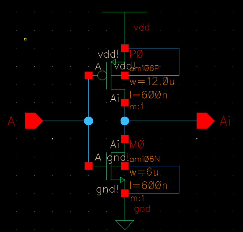
Now we can begin going through Tutorial 3 to make a schematic, symbol, and layout of an inverter.
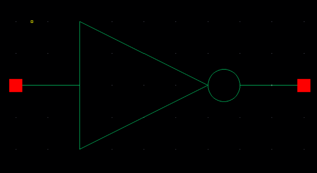
First we will create a inverter schematic, then create symbol to represent an inverter.
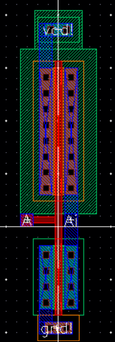
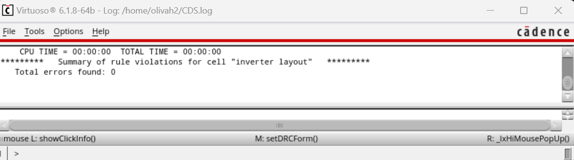
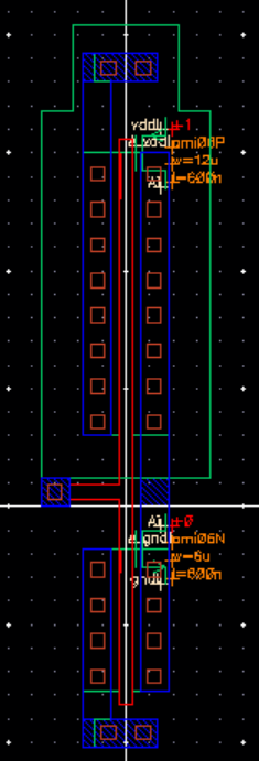
Next, we will create a layout of the inverter, then we will DRC check.
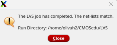
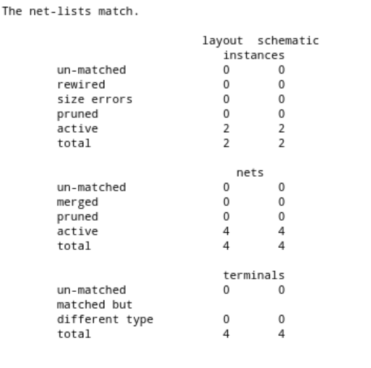
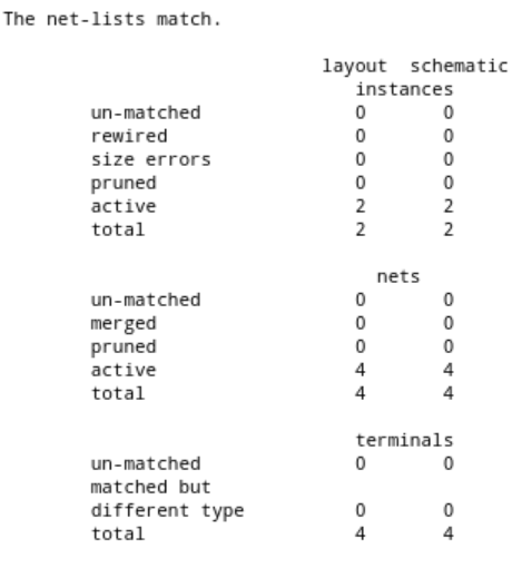
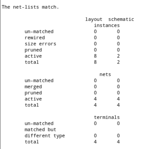
Now we will extract the layout and LVS it.
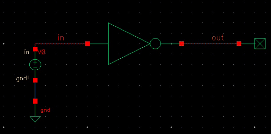
The next step will be to simulate to see the invertors operation. First create a schematic and then setup the simulation.
Below we can see the results of our simulation.
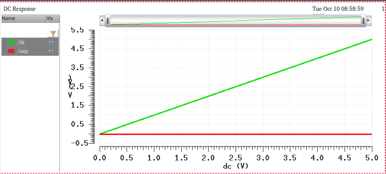
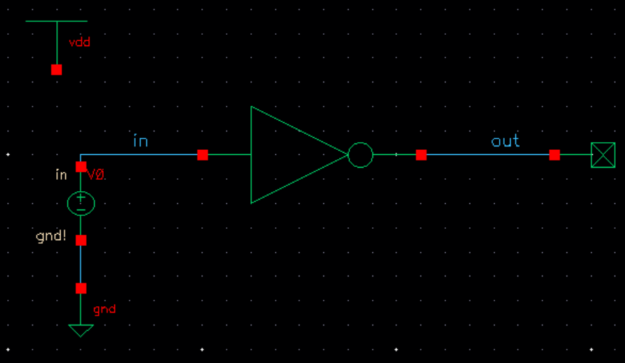
Next, we will add vdd because we did not include in the previous schematic.
Next, we will run a simulation of the circuit with a voltage.
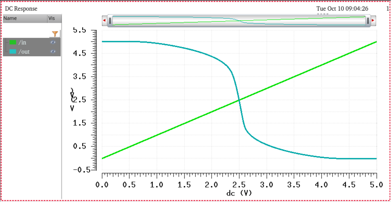
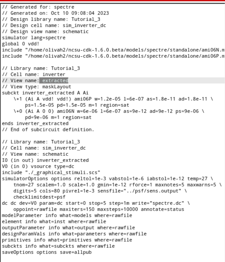
The final step is to a simmulation with the extracted, the results will be the same.
Lab:
We are going draft a schematic, layout, and symbols for two inverters
12u/6u Inverter
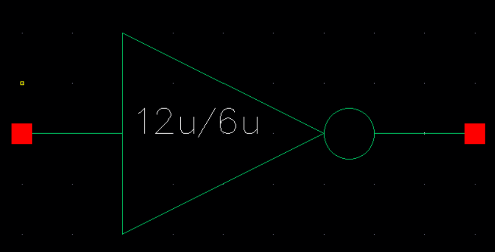
First, create a schematic of the 12u/6u inverter, then create a symbol for the inverter.
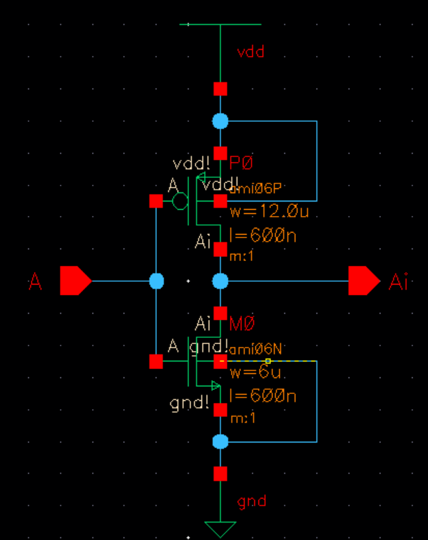
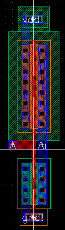
Next, create a layout of the inverter.
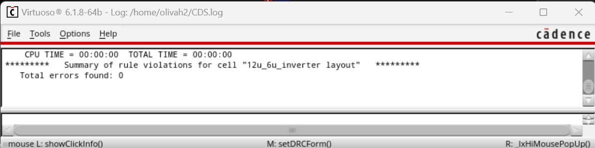
Next, we will DRC the 12u/6u inverter, and then extract the layout and LVS it.
Next, we will create a schematic for simluating the inverter.
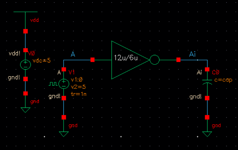
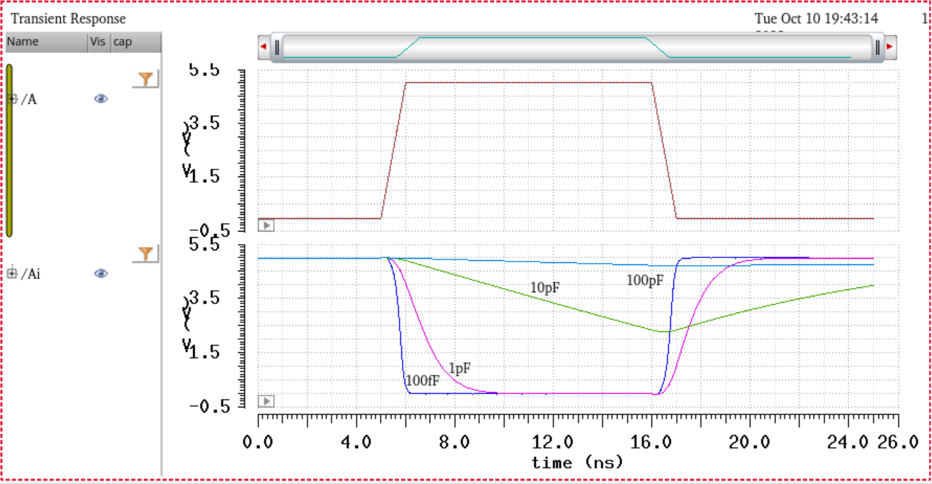
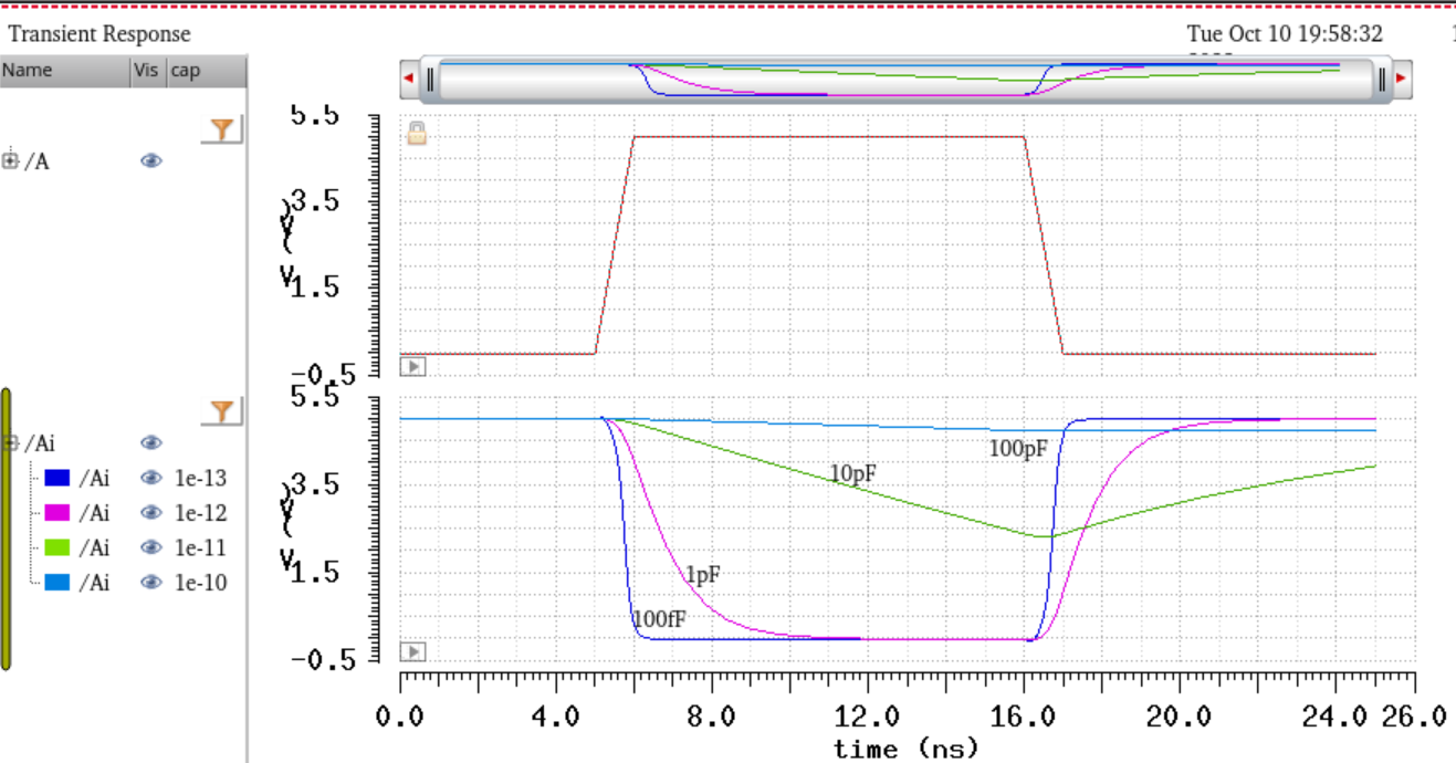
Next, we will simulate the 12u/6u inverter as Spectre simulation and Ultrasim simulation with the capacitive loads of 100fF, 1pF,
10pF, and 100pF.
Spectre Simulation
Ultrasim Simulation
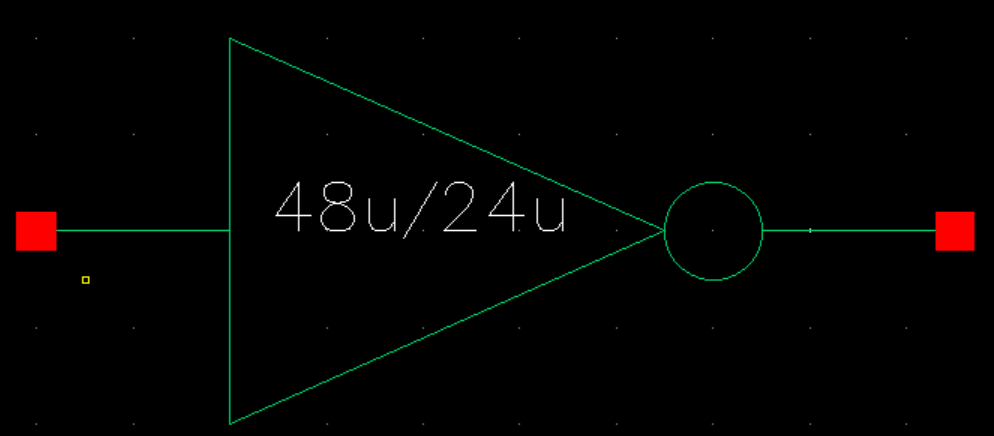
48u/24u Inverter
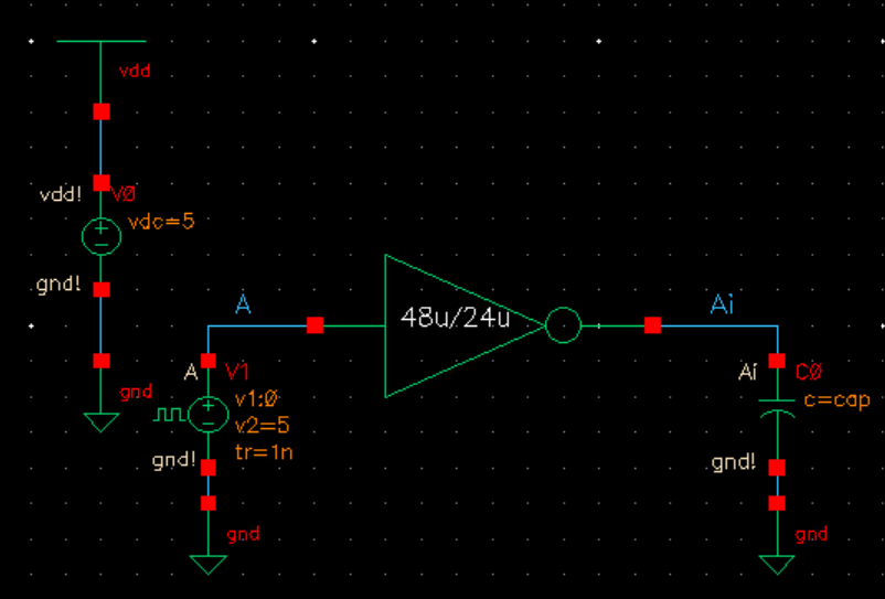
Now we will create a schematic of a 48u/24u inverter, then create a symbol for the inverter.
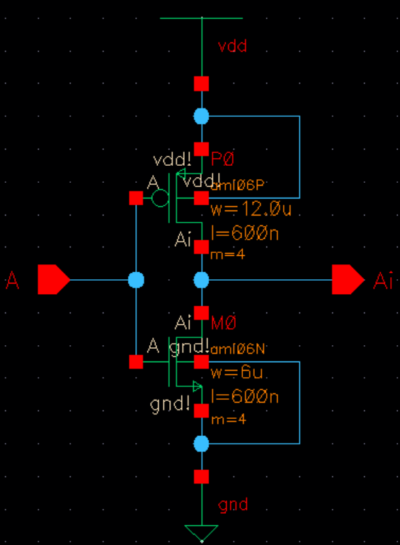
Next, we will create a layout of the inverter.
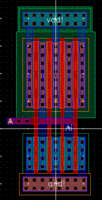
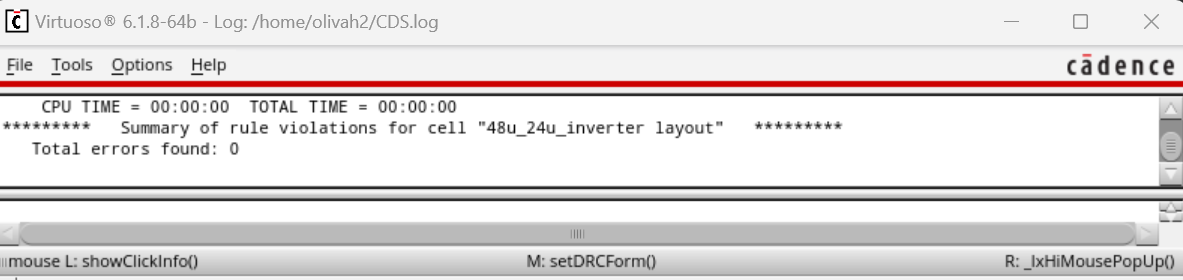
Next, we will DRC the layout. Then extract the layout and LVS it.
Next, we will create a schematic for simulating the inverter.
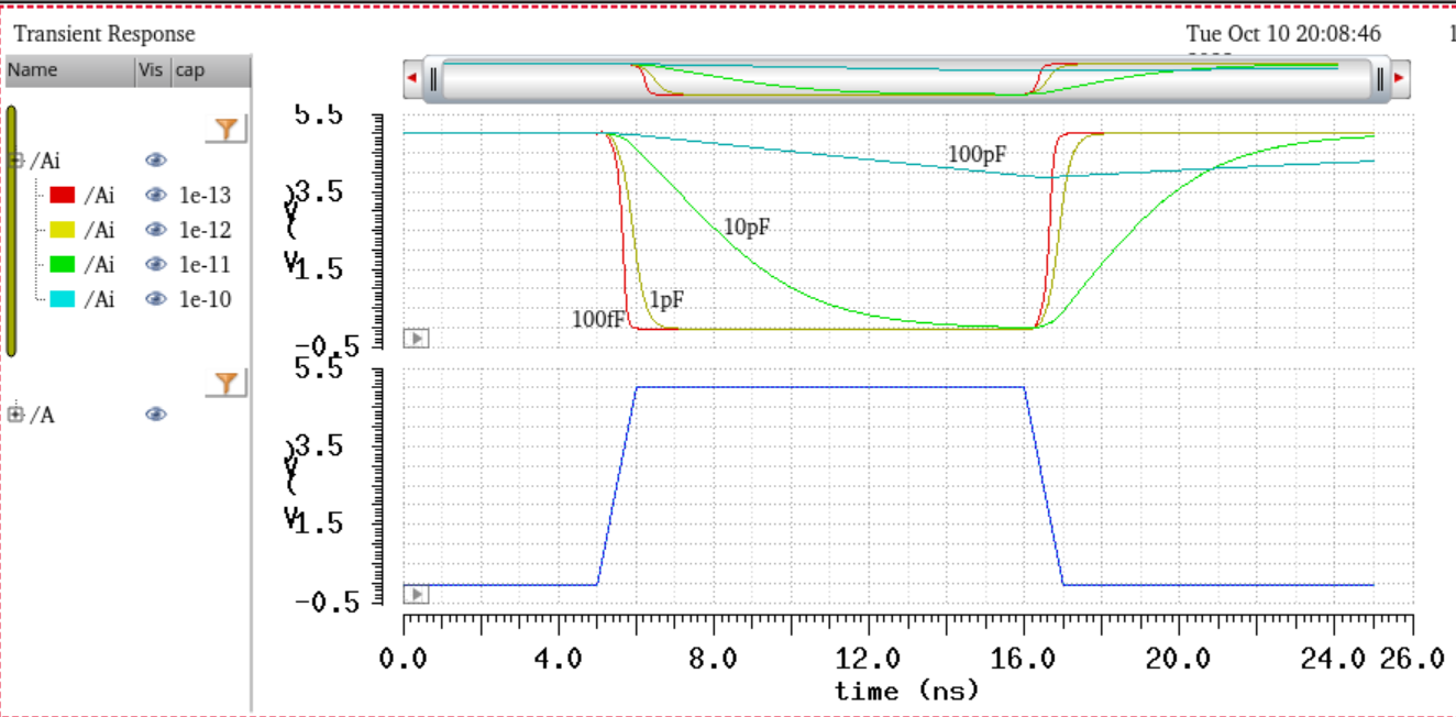
Next, we will simulate the 12u/6u inverter as Spectre simulation and Ultrasim simulation with the capacitive loads of 100fF, 1pF,
10pF, and 100pF.
Spectre Simulation
Ultrasim Simulation
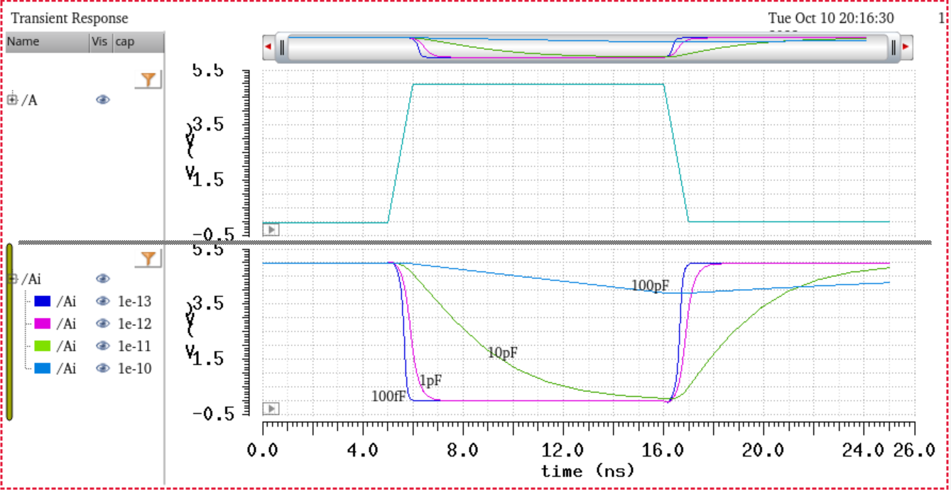
From our simulations, it can be seen that the higher the capacitance on the load, the slower the transition will be for the output.
The 48u/24u inverter has a faster transition due to it having a increased size, this will mean that the resistance will decrease.
The lab files for this lab are down below.
Files are Backed-up
Return to EE 421L Labs