Lab 4 - ECE 421L Fall 2023
Pre-lab:
We are to go through Tutorial 2 for the pre-lab.
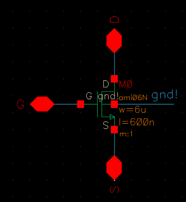
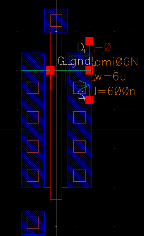
The first thing we do in the tutorial is copy Tutorial_1 into a new library named Tutorial_2, then create a Cell View called NMOS_IV within the new library. Now we open the schematic and press i (Instance), then select nmos4 in NCSU_Analog_parts library, making sure to set the transistors width to 6u and the length 600n. Now we place 3 pins to represent Drain, Gate, Source, and draw a wire for ground.
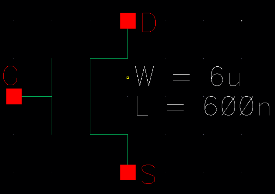
Then we save the schematic and create a symbol. Once the symbol has been made, we then delete everything in the cell except the
pins, and draw a MOSFET symbol.
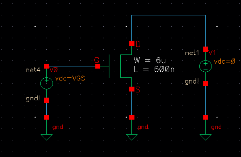
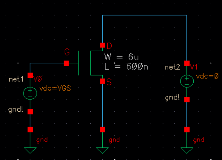
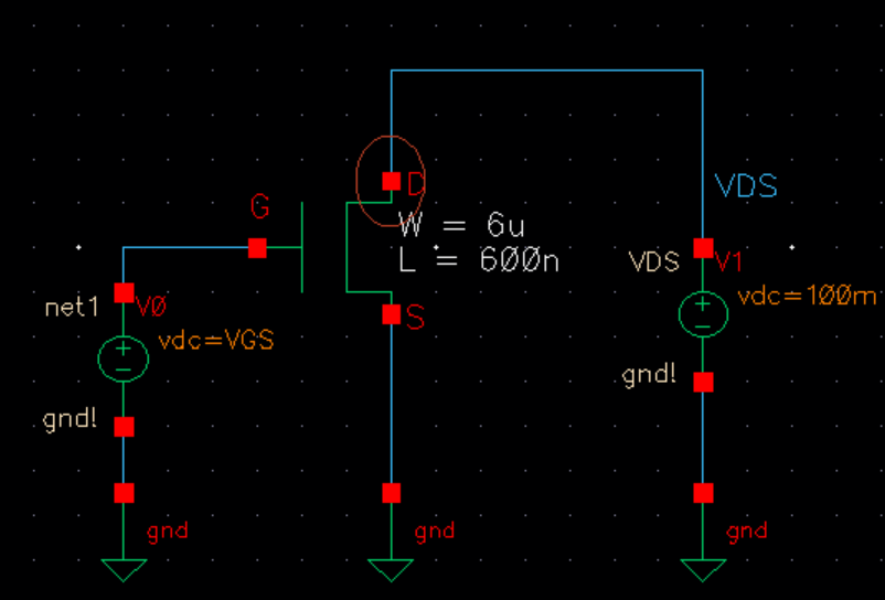
Check and save the symbol we made, and now create a new schematic for simulating. In this schematic we will set the value of V0
to VGS and the value of V1 to 0.
Now launch the ADE. Once it has opened we select Setup -> Model Libraries, making sure to select ami06N.m since we are doing
NMOS model. Next hit OK, then go to Variables - > Edit and add VGS, setting the value to 0. Now setup the analysis parameters,
and select the output to be pin D on the schematic. Go Tools -> Parametric Analysis and set the parametersr for it, make sure to
save the state.
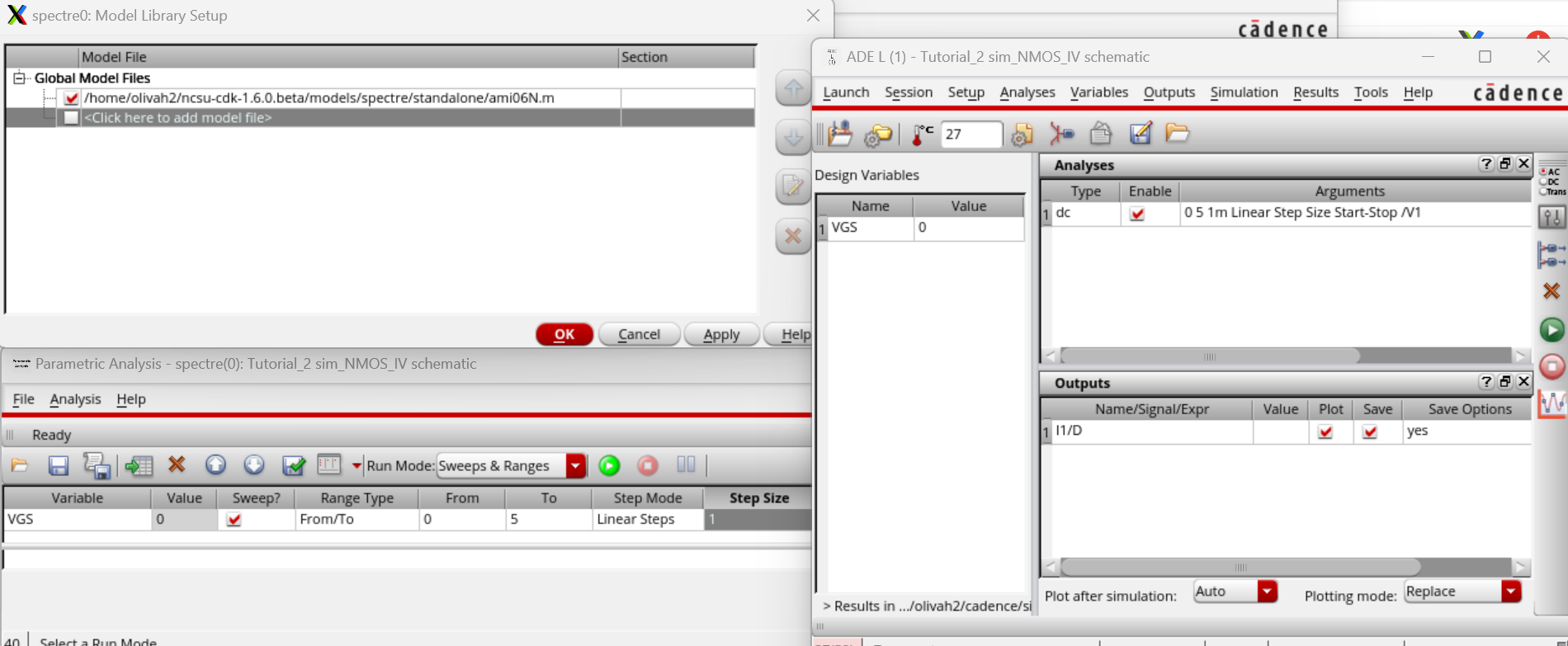
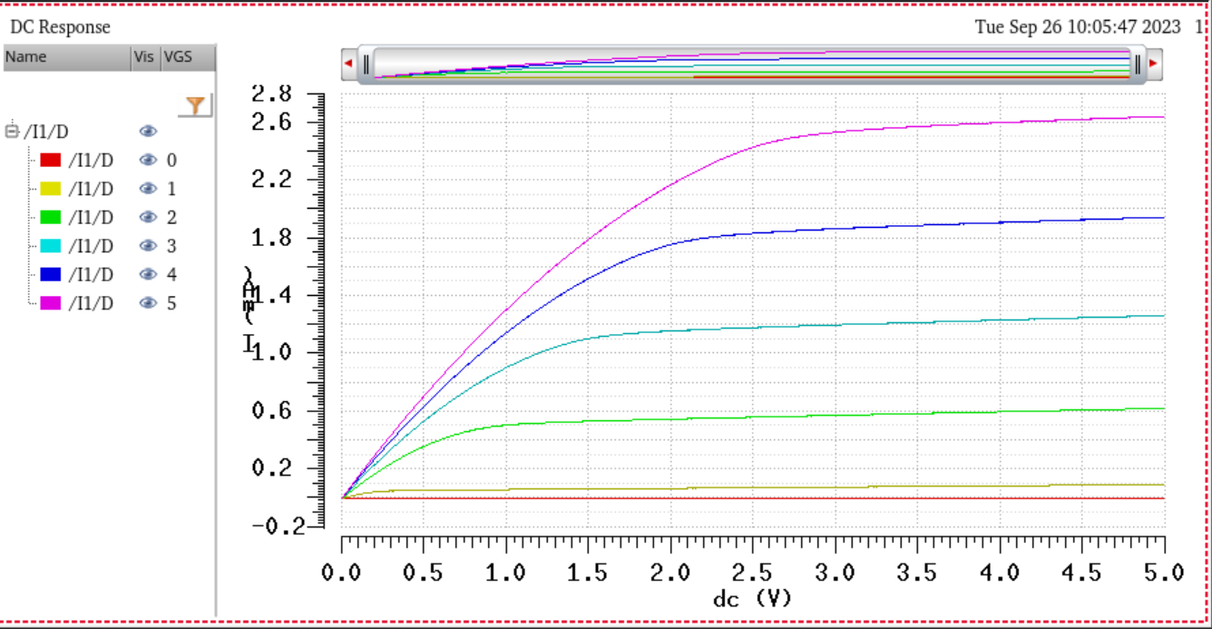
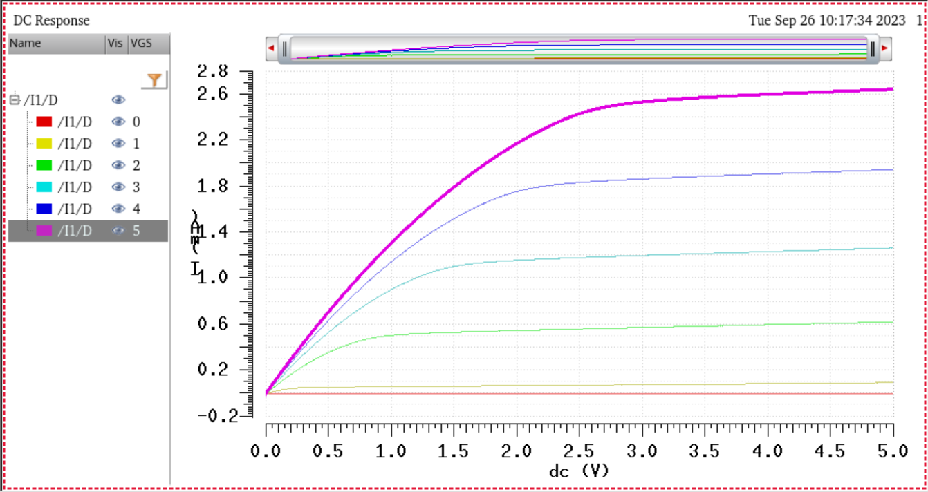
Now, press the green button and the shcematic should work. It should appear as it is below.
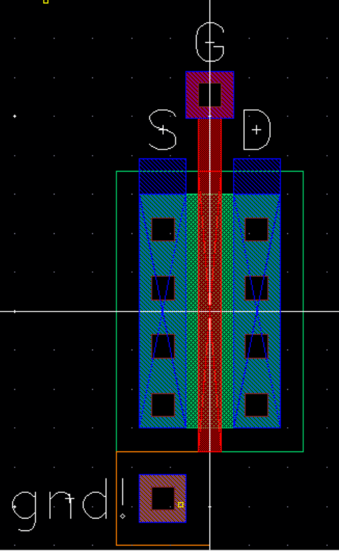
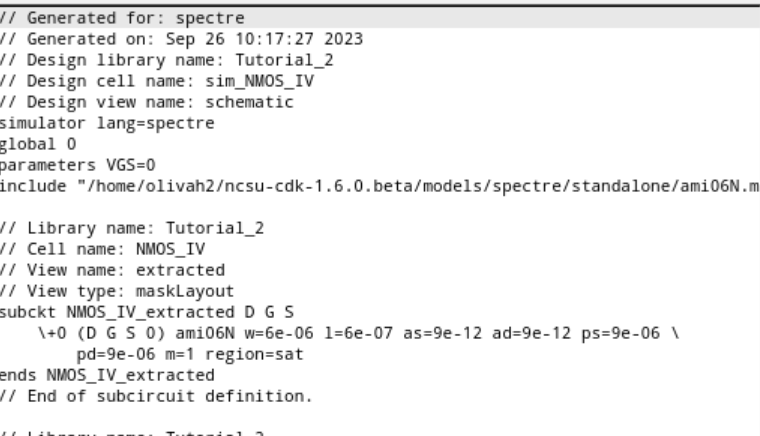
Following the simulation, close everything and create a new layout view in NMOS_IV. An important note is that we have to add the
ptap cell and m1_poly, then use metal1 to place the pins for the layout. Once the layout is finished, then extract the it.
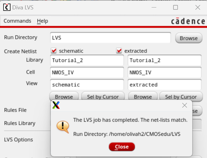
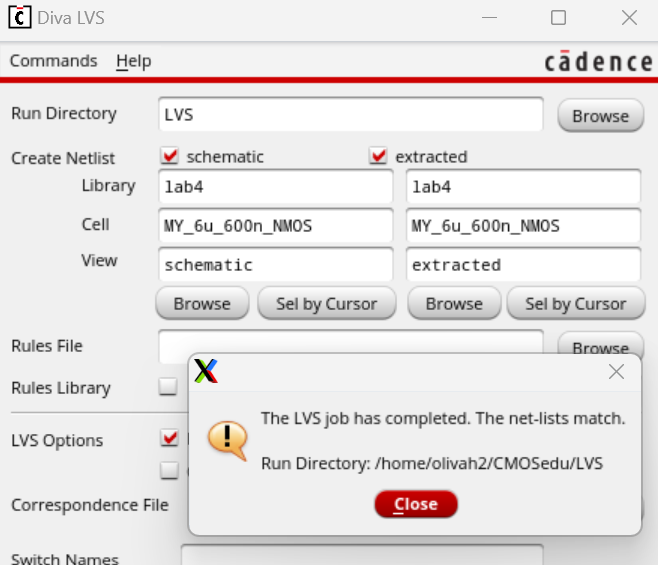
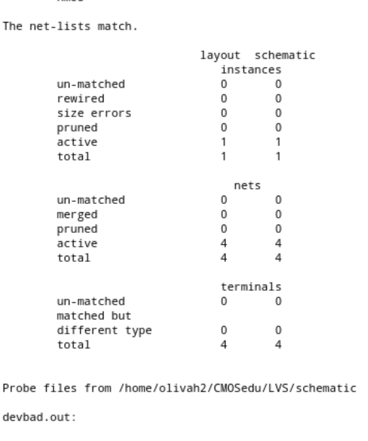
Next, we LVS the schematic and extracted view.
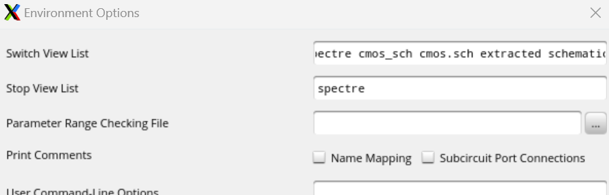
Now go back to the simulated schematic and launch ADE. Load the state we saved before. Go to Setup -> Environment and add
extracted.
Then run the parametic analysis again. Which should be the same as before.
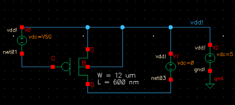
For the next part tutorial, we will repeat the same steps as before, but instead of NMOS it will now PMOS.
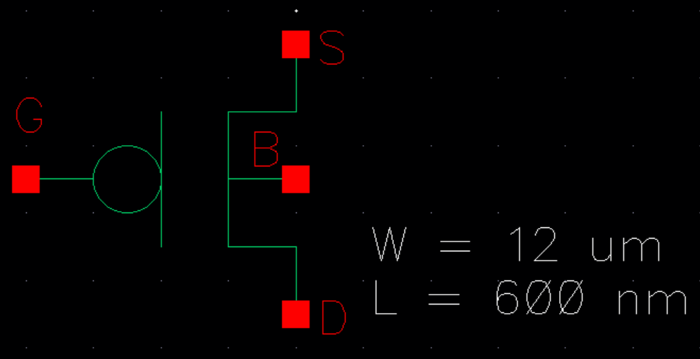
First create a PMOS schematic with the width to 12u and length to 600nm.
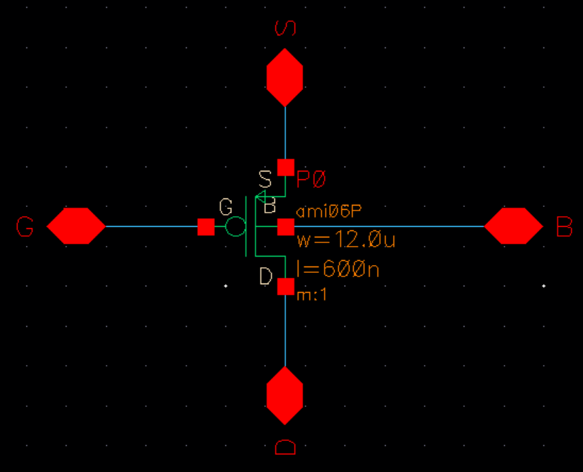
Once we finish the schematic, we then create the symbol for our schematic.
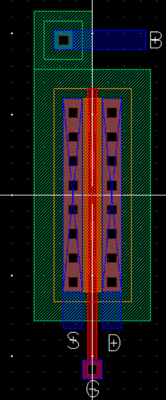
Next, make the layout for the PMOS.
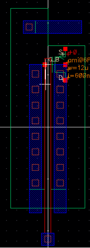
Now, extract the layout.
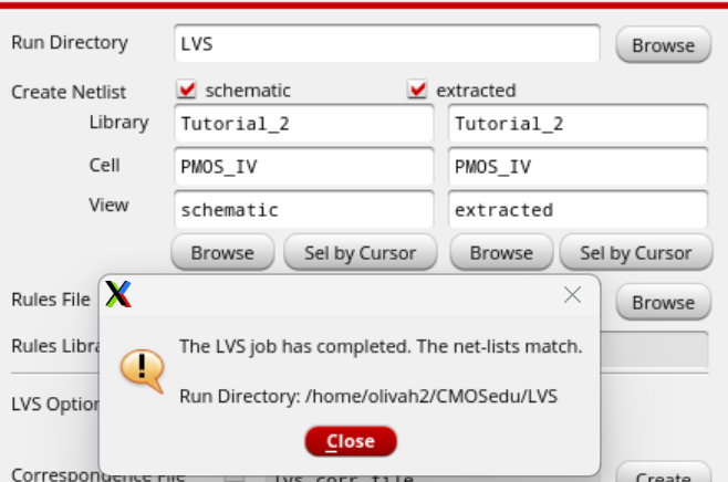
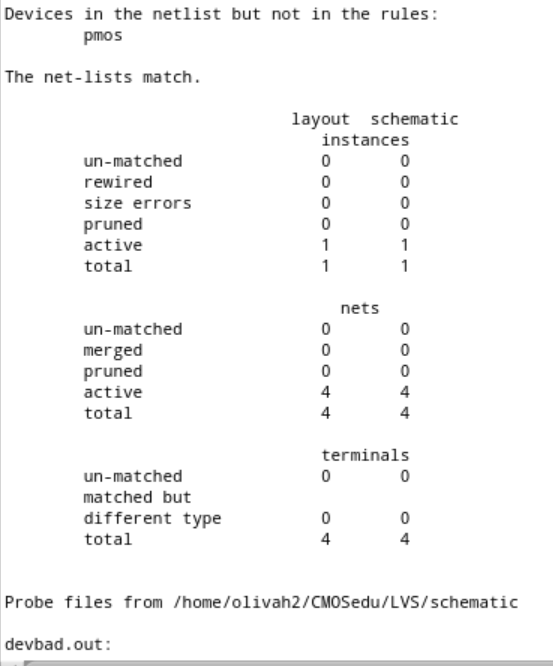
Now, LVS the schematic and extracted view of the PMOS.
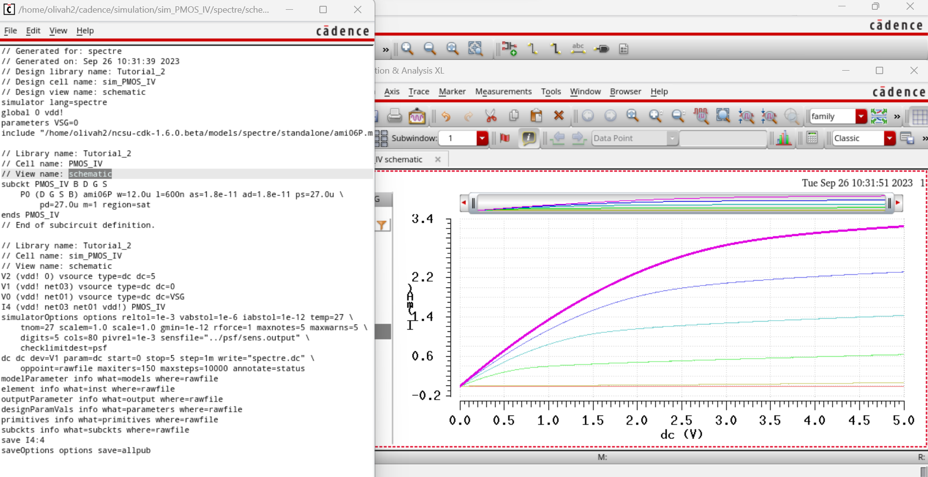
Next, create a schematic for our PMOS to simulate.
Now, simulate the circuit, using a similar setup process as before. Below are the results of the schematics simulation.
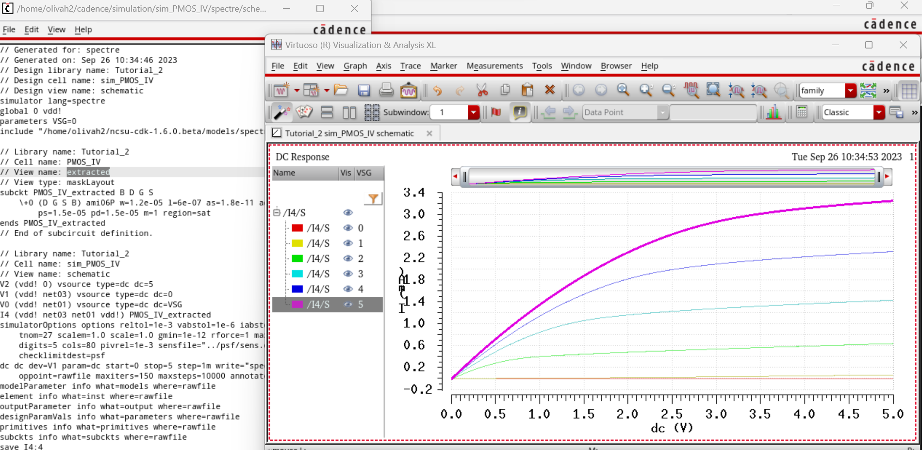
Below we can see the results of the extracted layout.
Lab:
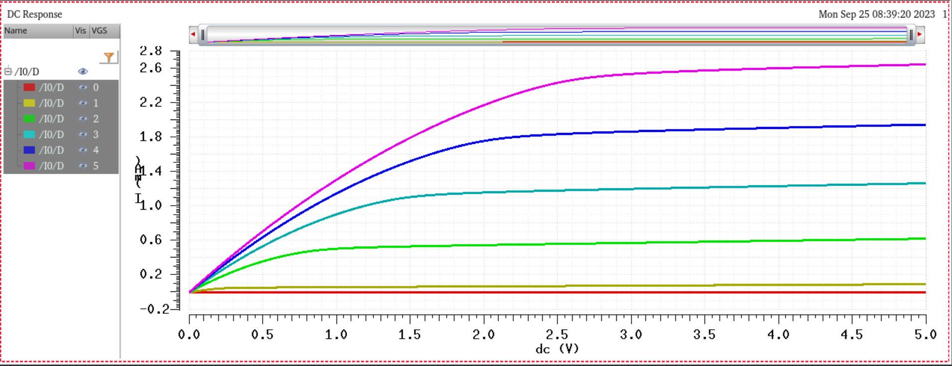
A schematic for simulating ID v. VDS of an NMOS device for VGS varying from 0 to 5 V in 1 V steps while VDS varies in 1mVsteps. Use a 6u/600n width-to-length ratio.
Simulate the schematic as we did in the prelab agian.
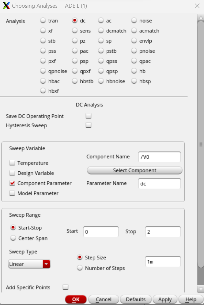
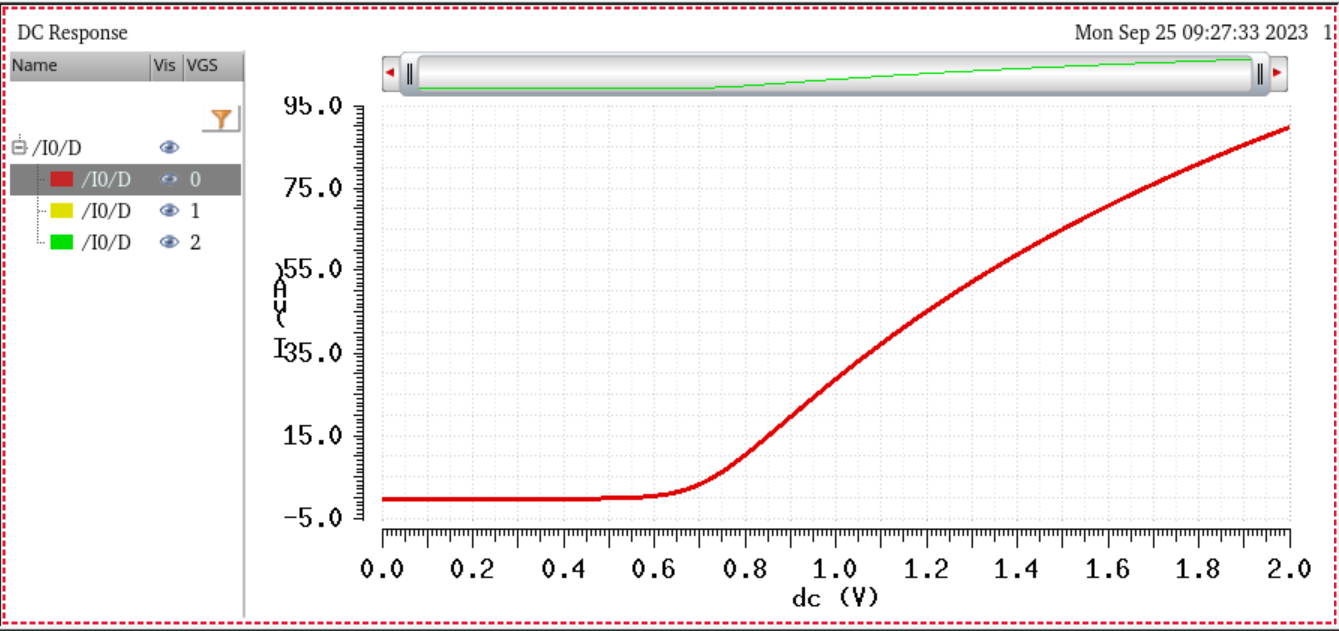
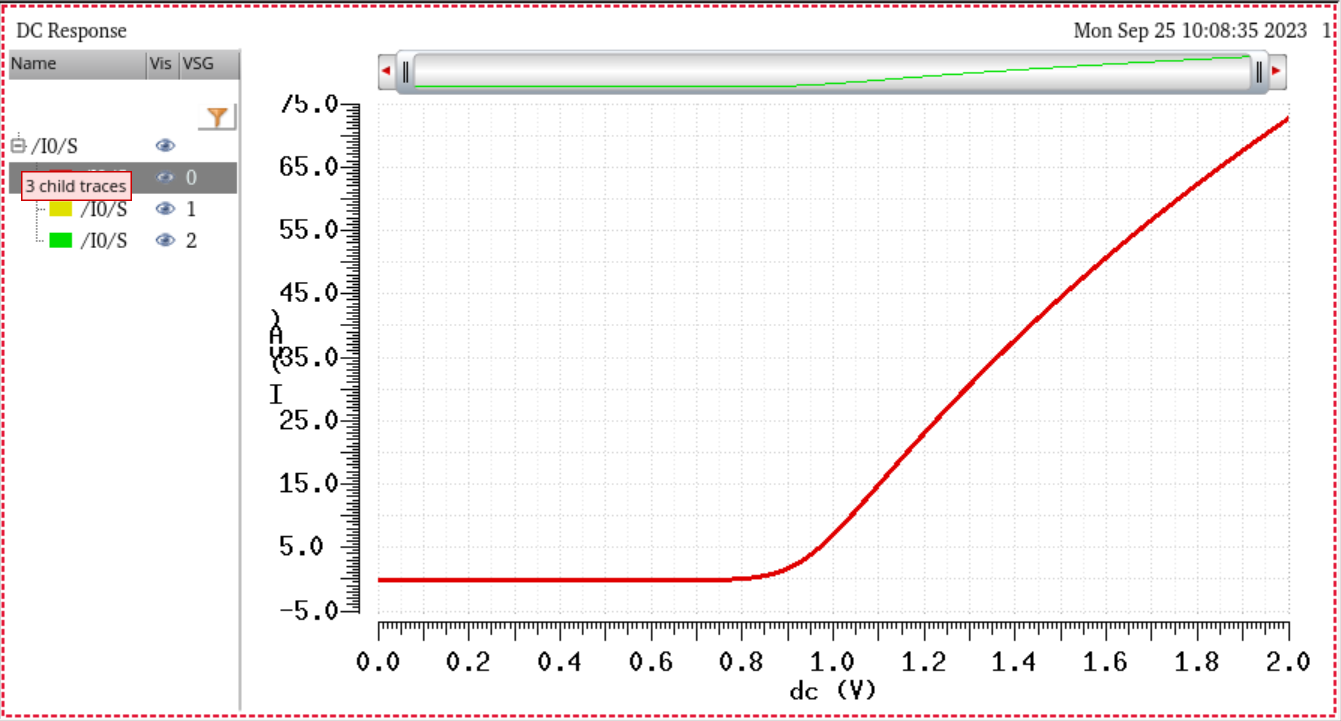
A schematic for simulating ID v. VDS of an NMOS device for VDS = 100 mV where VGS varies from 0 to 2 V in 1mV steps. Again use a 6u/600n width-to-length ratio.
Set the following for the analysis. Then run the simulation.
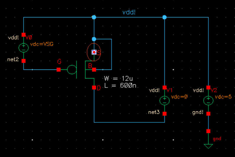
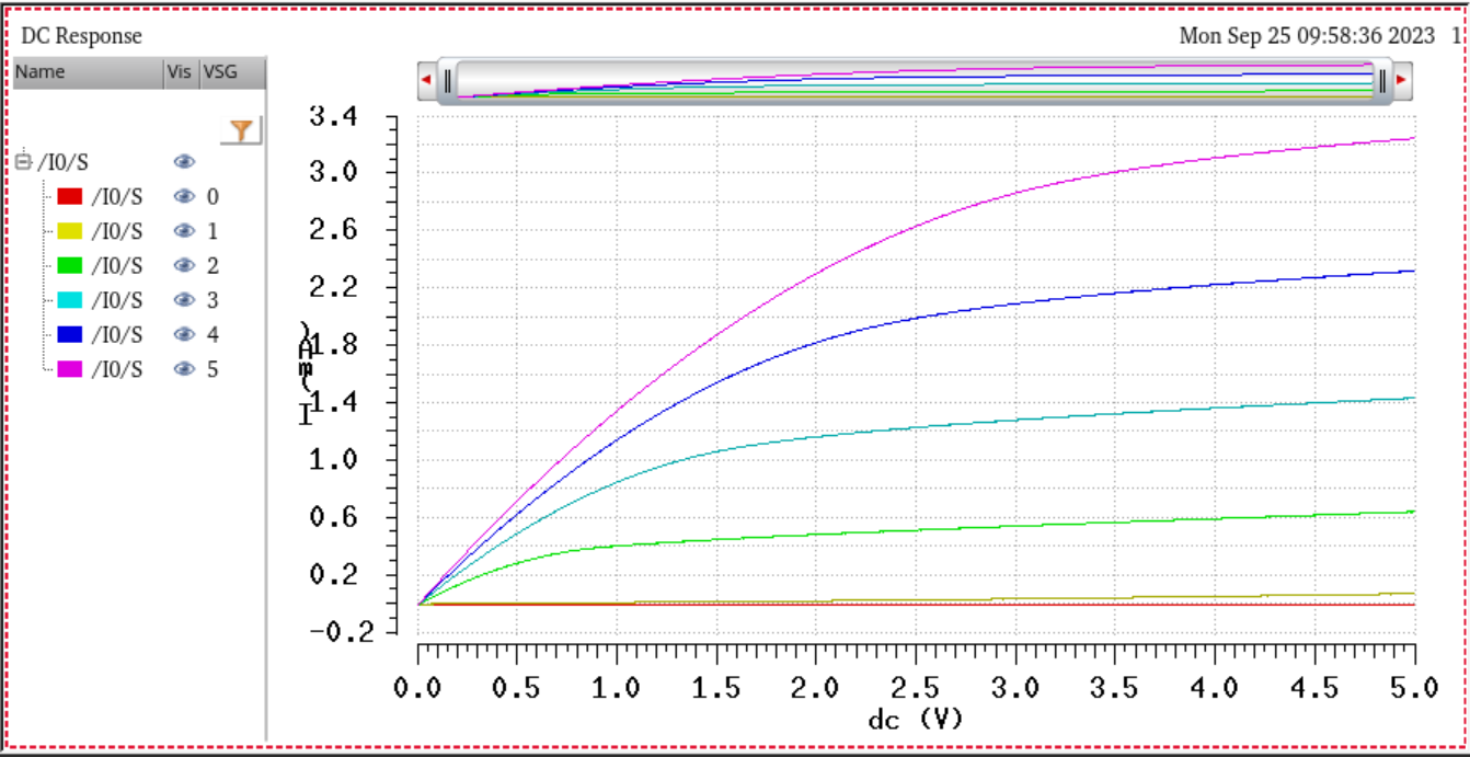
A schematic for simulating ID v. VSD (note VSD not VDS) of a PMOS device for VSG (not VGS) varying from 0 to 5 V in 1 V steps while VSD varies from 0 to 5V in 1 mV steps. Use a 12u/600n width-to-length ratio.
Simulate the schematic as we did in the prelab agian.
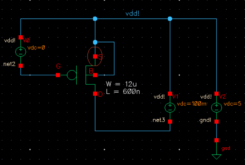
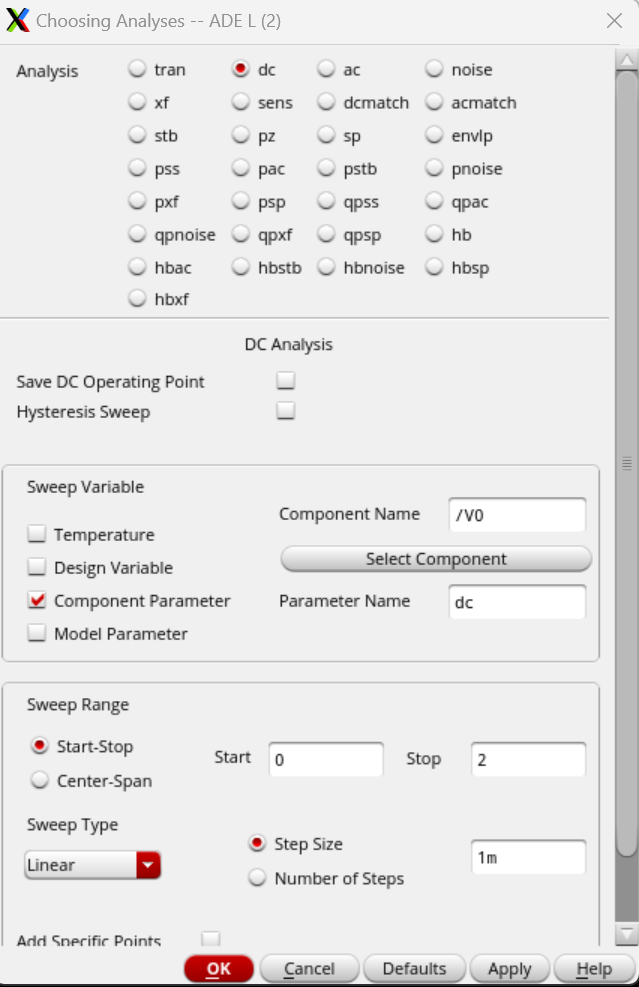
A schematic for simulating ID v. VSG of a PMOS device for VSD = 100 mV where VSG varies from 0 to 2 V in 1 mV steps. Again, use a 12u/600n width-to-length ratio.
Set the following for the analysis. Then run the simulation.
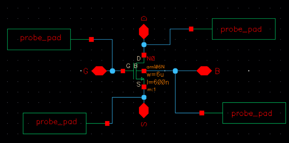
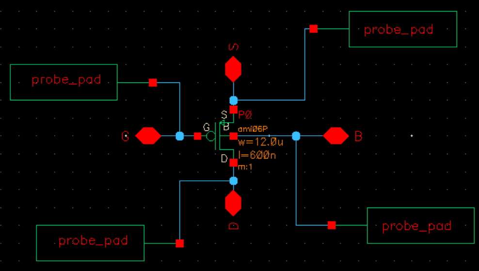
Layout a 6u/0.6u NMOS device and connect all 4 MOSFET terminals to probe pads
Create a MOSFET schematic with probe pads.
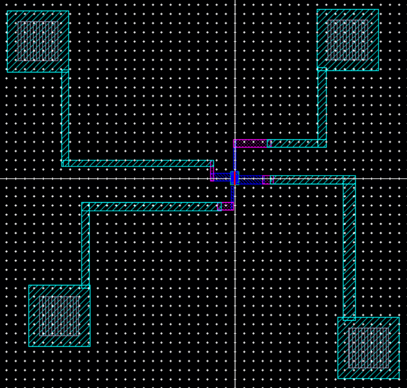
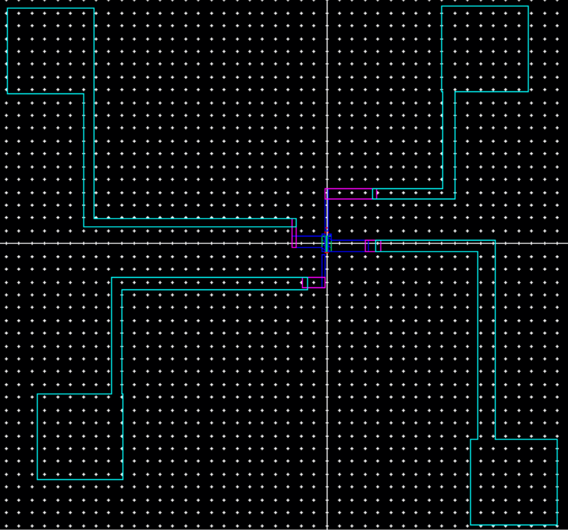
Then create a layout of the NMOS with the probe pads. After its made, DRC check it.
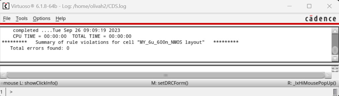
Following DRC having zero errors, we will extract the layout and then LVS the schematic and extracted view.
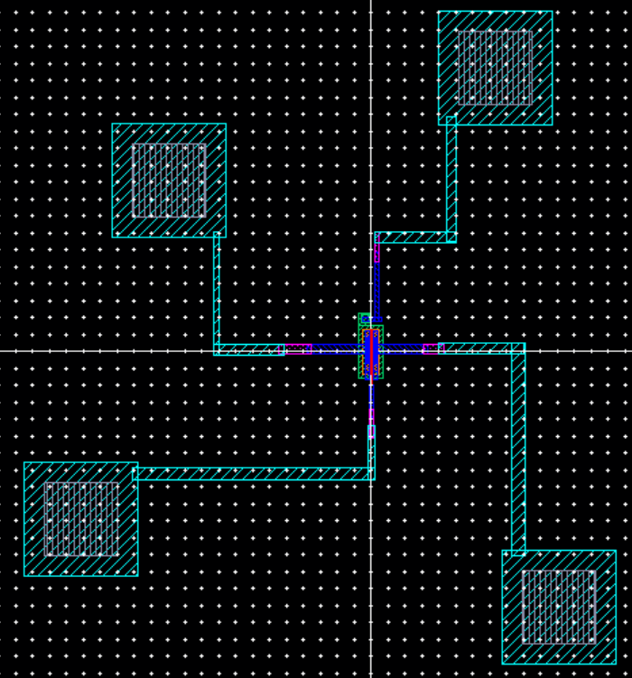
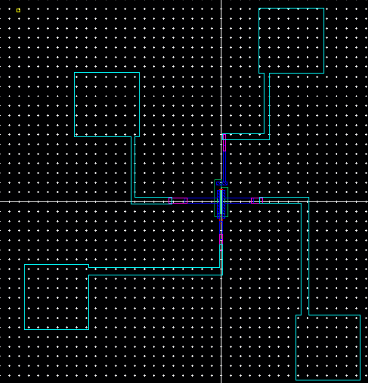
Layout a 12u/0.6u PMOS device and connect all 4 MOSFET terminals to probe pads.
Now we do the same process as before, but instead of NMOS its with PMOS.
Next create a PMOS layout with probe pads. After its made, DRC check it.
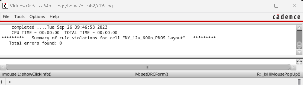
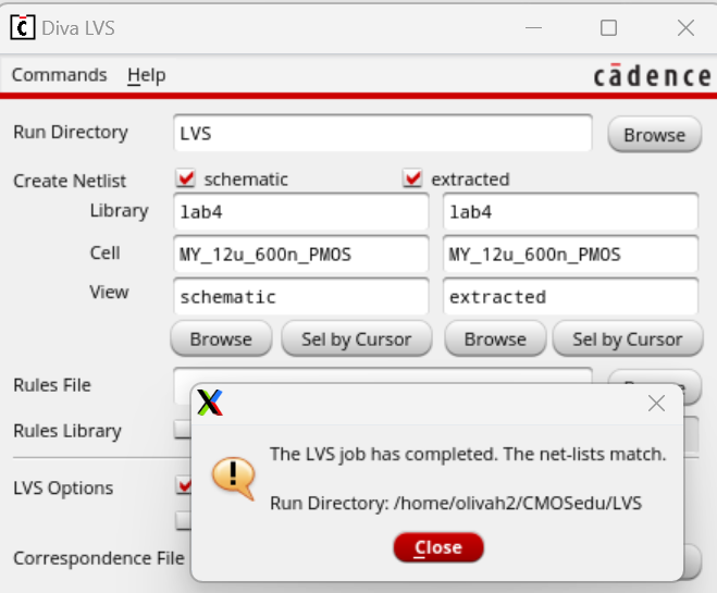
Following DRC having zero errors, we will extract the layout and then LVS the schematic and extracted view.
Back-up Files
Return to EE 421L Labs