Lab 2 - ECE 421L Fall 2023
Lab 2 - Design of 10 bit Digital-to-Analog Converter
Pre-lab:
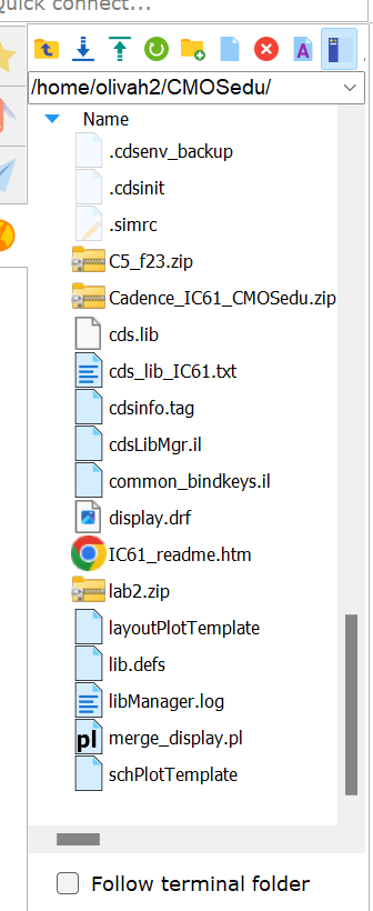
The Prelab first wants us to download lab2.zip, then to upload the file to CMOSedu directory,
following this we unzip the file.

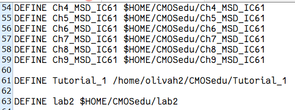
The next step is to open the text editor for cds.lib and add the line DEFINE lab2 $HOME/CMOSedu/lab2
to access it within cadence.
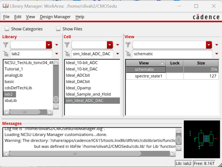
Now start Cadence, then scroll through the Library Manager for lab2. Once found then
select sim_Ideal_ADC_DAC and open the schematic.
Now that the schematic is opened, Launch ADE, go to Session -> Load State -> Cellview -> OK.
Press the green button to simulate the schematic.
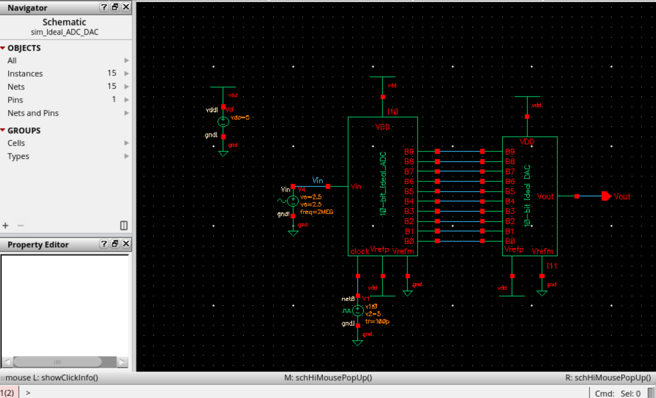
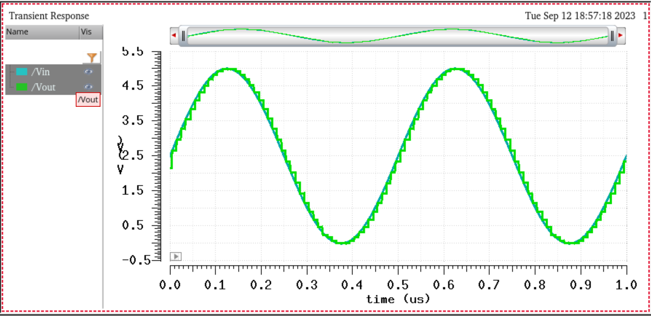
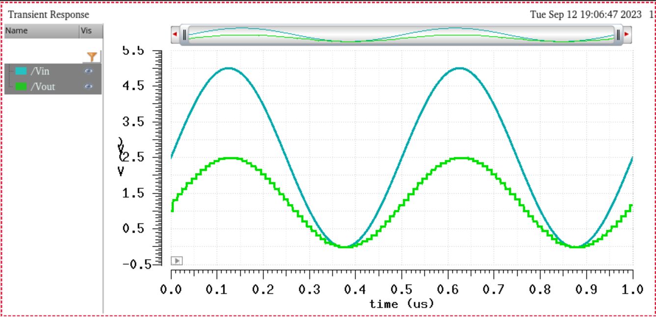
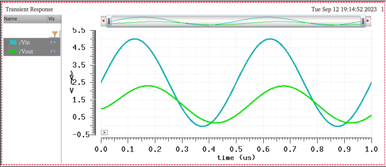
After simulating the schematic, we can see the Vin and Vout waveforms.
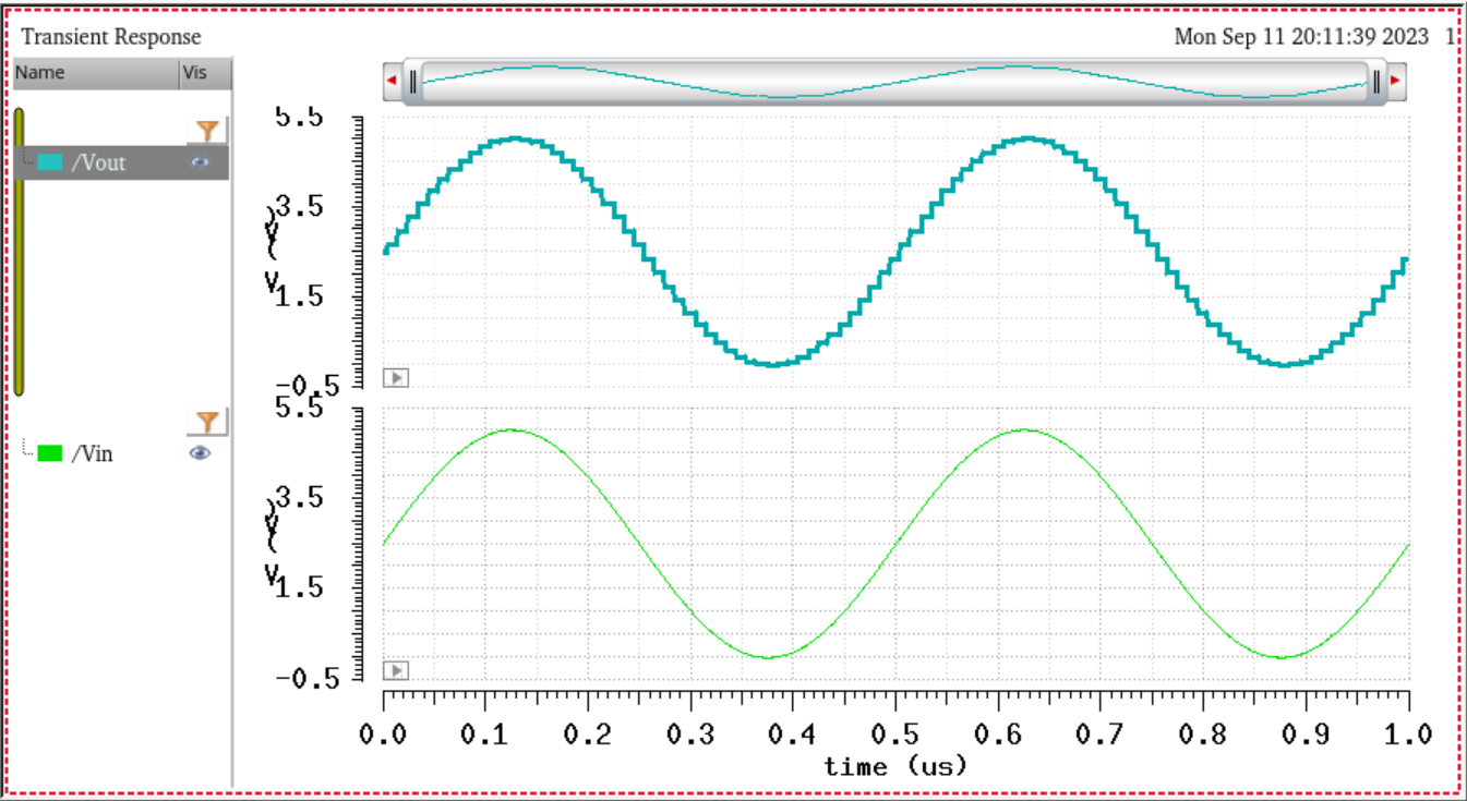
Results from different simulation
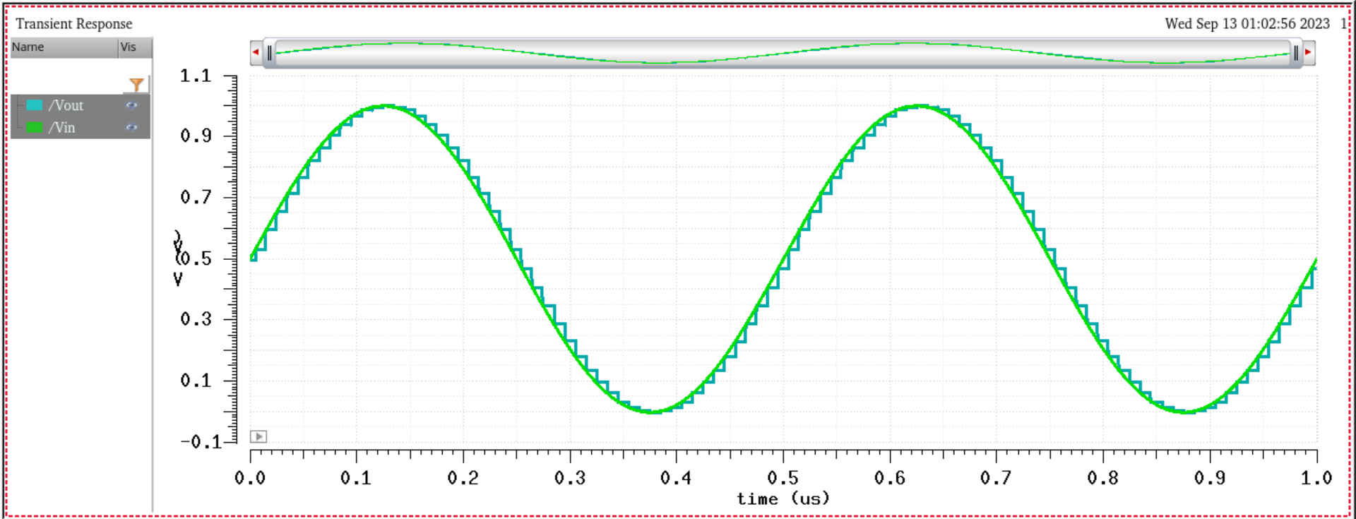
Illustrating my understanding of ADC and DAC, by changing the amplitude and offset of the input to 500mV. It can be seen that
the range of the steps of the output has decreased.
Determine the Least Significant bit (LSB)
The Pre-lab gives us the equation 1 LSB=VDD/2^n, which will give us the LSB. Lets fill in the values, VDD=5V, the number of
outputs will determine the n. In this case n=10 because the 10-bit output. This will then mean LSB= 5V/2^10 =4.88mV.
Lab:
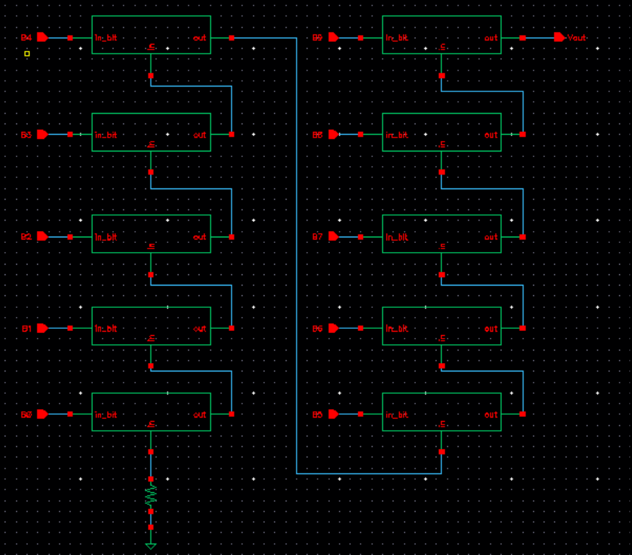
In this lab we will design a 10-bit DAC using an n-well R of 10k.
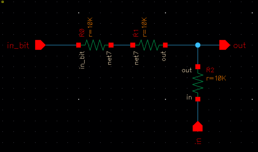
The first thing to do is create a voltage divider representing the Figure 30.14. This is done with 3 10k resistors and creating
three pins as in, out, in_bit.
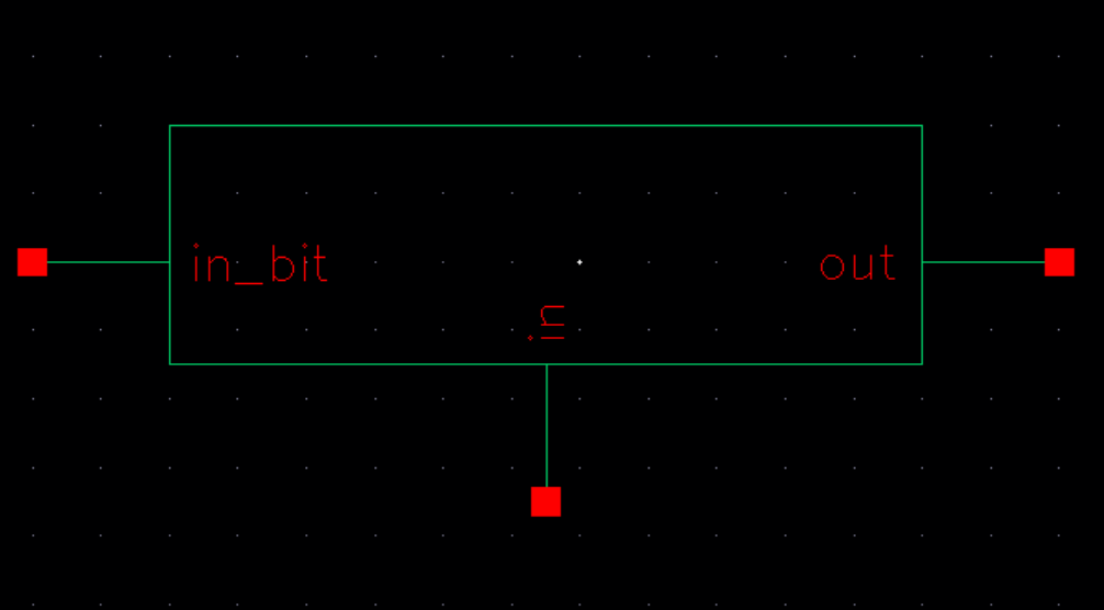
Following the schematic create it as a symbol by going to Create -> Cellview, then select cellview and hit OK. This will then
open a new window that is your symbol.
Following this symbol close the window, and create a new schematic. Then press I and select the library with the above symbol
and place 10 of them. Once done add a 10K resistor and ground, create pin labels, and connect them to each other with wires. Then
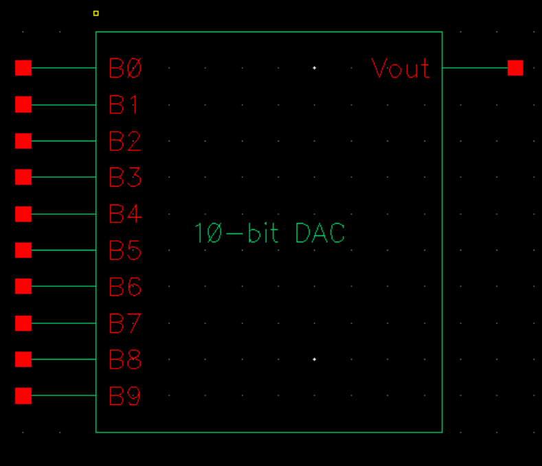
create this schematic as a symbol like before.
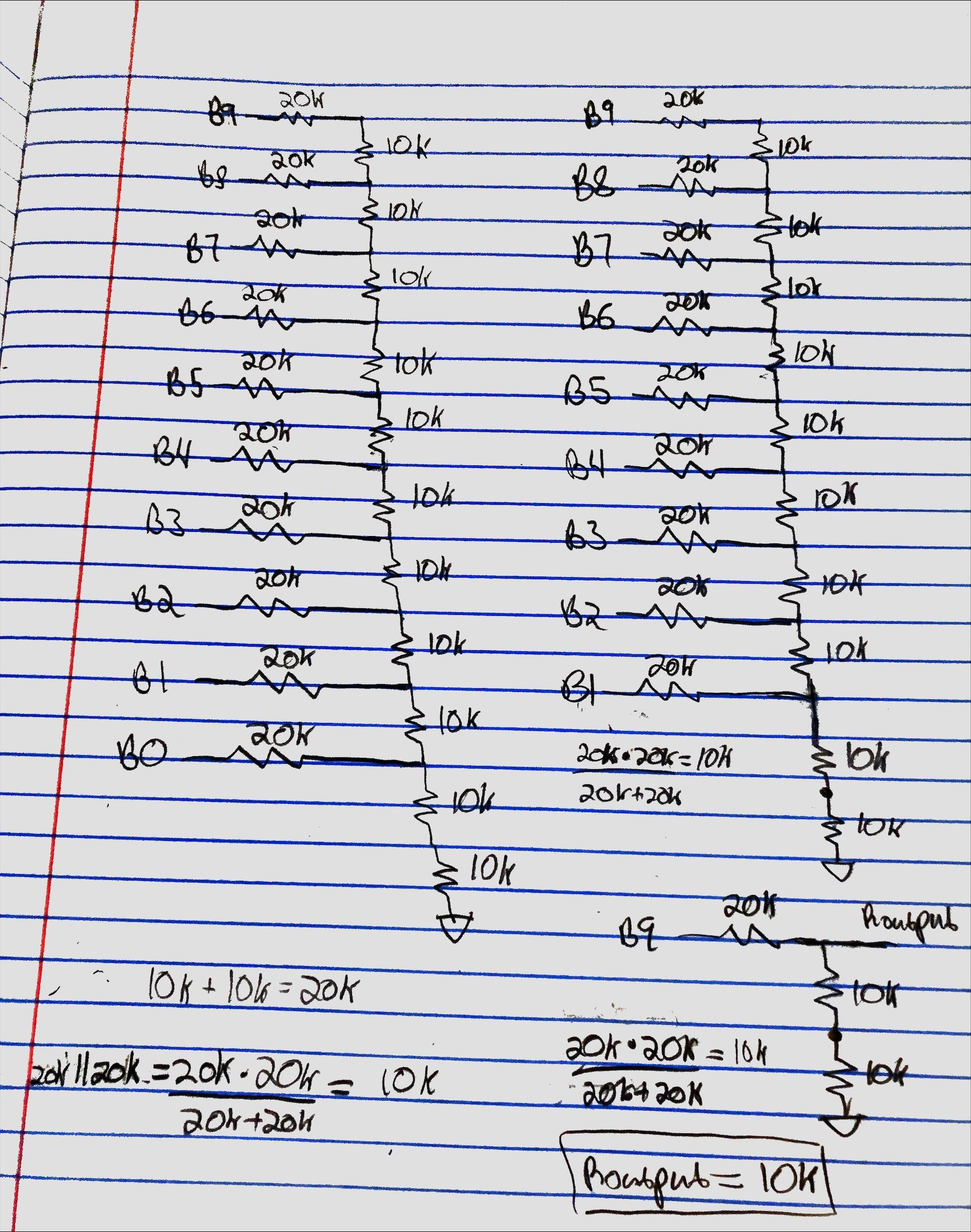
Determine output resistance of the DAC
Below we can see the schematic that was drawn. The first thing we did was add the two 10k ohm resistor equaling 20k ohm resistor.
From here we will take the two 20k ohm resistors in parallel, resulting in 10k ohm resistor. This will then change schematic, similar to what it was before but slightly differnet.This calculation is repeated with our DAC and we get an output resistance of 10k ohms.
Determining Delay, driving a load
The equation we are given for to delay is 0.7RC. R will be 10k ohm and the delay of the DAC is 10pF load. This information will be plugged into the equation, as we see below.
0.7(10k)(10p) = 70ns
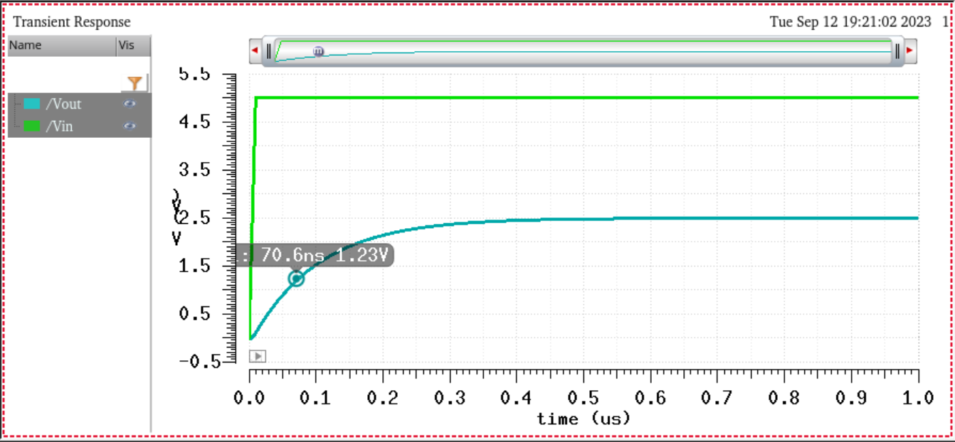
To verify the time delay from above, we will create a schematic by grounding the B0 through B8. Then adding a voltage source to B9 and a capacitor that is set to 10pF.
The next thing to do is verify the delay by simulating it. The first thing is to ground the B0 through B8 inputs, then take the pulse
source and connect it to B9. Then add the capacitor to the output.
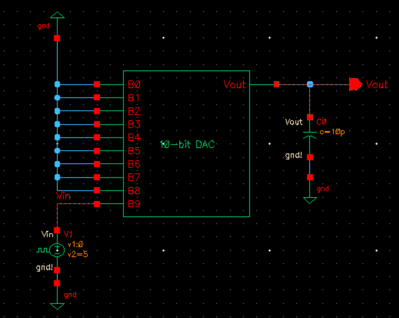
Below we can see the simulation and how the output is 2.5V, as well as the time delay measurement is 70ns.
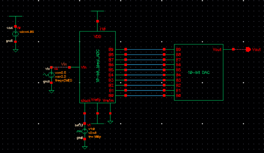
Simulation for Verifying design functions
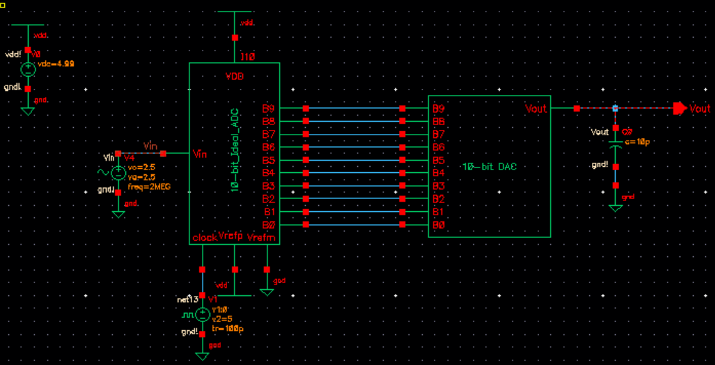
The first thing we did was replace the DAC from the sim_Ideal_ADC_DAC with the one we designed. Once this was done we
simulated it. There was a change with the VDD=4.99 to save the simulation.
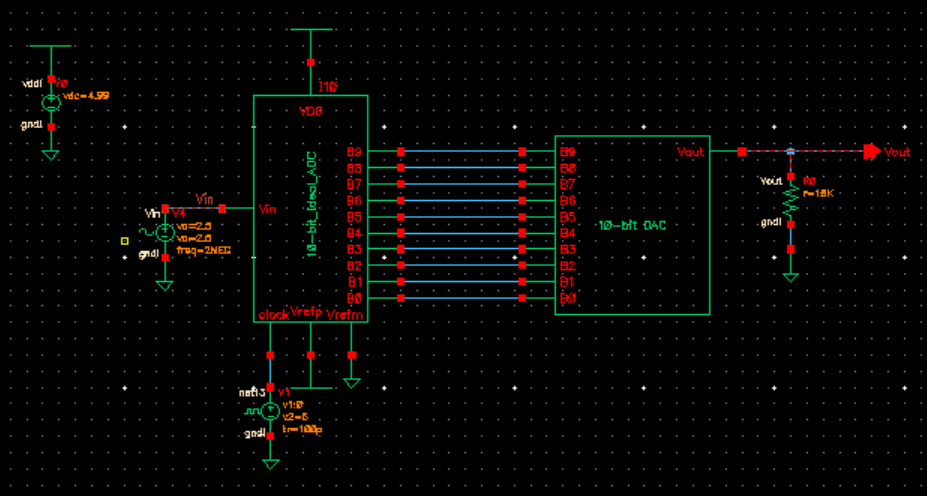
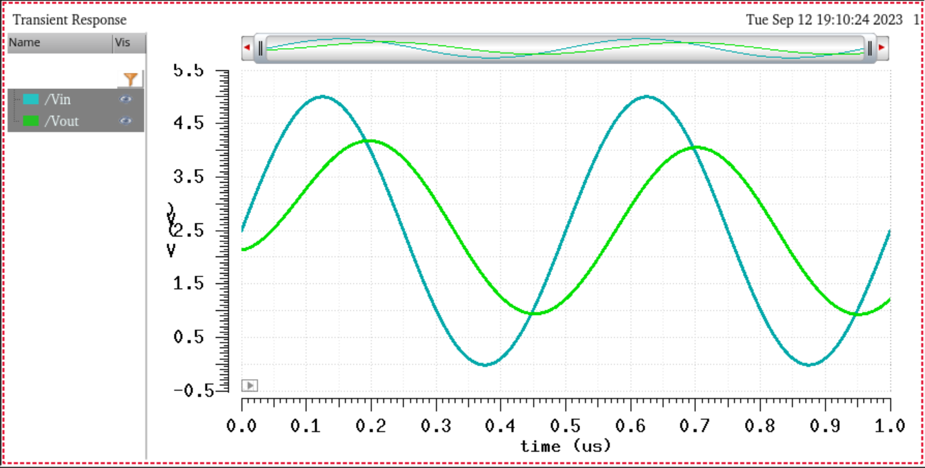
The next simulation we did was with a resistive load of 10k ohm. It can be seen that the 10k ohm load becomes a voltage divier with
the output of 2.5V.
The next simulation is a capacitive load that will be 10pF. After adding this to the schematic we can see that the output is not a
pulse anymore. The other thing we can see is that there is lad with the output.
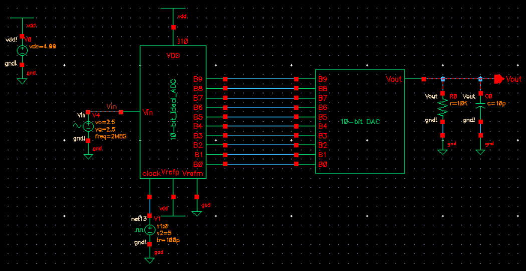
The final simulation is including a RC load. This we now combine the individual pieces from the previous simulations to a single one.
We can see that the simulation output is not a pulse, is lagging, and that the voltage has now been halfed.
In a real circuit if the switches are not small compared to R, what happens?
Then R would be added throughout our calculations, resulting in the resistance equivalent being higher, which can lead to higher output resistance.