Lab Project - ECE 421L Fall 2023
Project requirements:
Design a non-inverting buffer circuit that will present less than 100 fF input capacitance to on-chip logic
and that can drive up to a 1 pF load.
The output voltages must have a voltage greater than 7V (an output logic 0 is near ground and and output logic 1 is greater
than 7V).
Assume VDD is between 4.5V and 5.5V, a valid input logic 0 is 1V or less, a valid input logic 1 is 3V or more. Show that your
design works with varying load capacitance from 0 to 1 pF. Assume that the slowest time allowed is 4ns.
_____________________________________________________________________________________
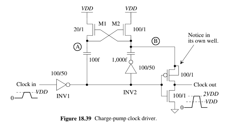
The first thing to do is to understand how to design our charge pump that we will use within our non-inverting buffer
circuit. The best way to understand the charge pump is to look at the Charge-pump clock driver circuit.
It can be seen that there is an input that will pass through the first inverter. For the input of the charge pump we will start
with logic 0 which is our low. When the 0 passes through the first inverter it will become 1 and flow through the wires. When
the logic 1 goes through the 100fF capacitance since it is at VDD is will then boost to 2VDD this will then turn on the M2 NMOS.
Going back to the after the first inverter the logic 1 will pass through the second inverter, which we will put the logic to 0. Now
that the logic is 0 the B node will be VDD which will turn M1 NMOS off with the charge pump. Then the logic 1 going though the
PMOS on the bottom right will be turned off, while the NMOS on the right will be turned on. The result will be that the output
is 0. For the case that the input logic is 1, when it passes through the first inverter it will become logic 0. Following the wire
through the first capacitance the A node will be VDD. Since the node A is VDD, it will mean that the M2 NMOS will be turned
off. Following the logic 0 through the second inverter the logic will become 1. This will result in the B node being 2VDD, which will
turn on the M1 NMOS. The logic 0 that is passing through the PMOS it will be turned on, while the logic 0 will turn off the
NMOS. This final output will be that it is 2VDD. This can be seen with the circuit below.
Now, that we understand the how the logics will work through the circuit we will begin with selecting the sizes of the our pmos and
nmos for the input. The equation and calculation can be seen below.
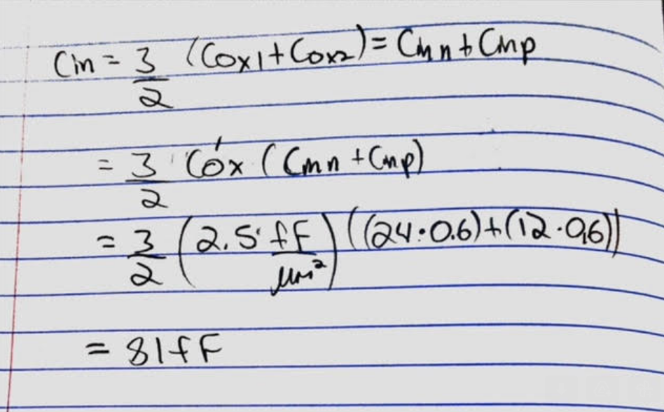
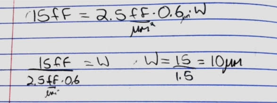
We can see above with the equation, we got less than 100 fF. This means that we are good for the requirment of the input being
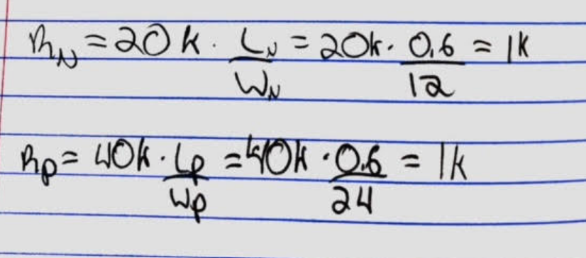
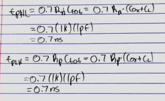
less than 100fF. Following this we will calculate the resistance for the pmos and the nmos. This will be needed for calculating
the time constant for discharging the load capcacitor that is known as tphl. It also will be needed for the calculating the time
constant with charging the load capacitance. The one other calculation we will need is the capacitor that we need for the A node.
These can be seen down below.
Now, that we have done our calculations we can continue by creating our schematic. The first thing to do is create a schematic
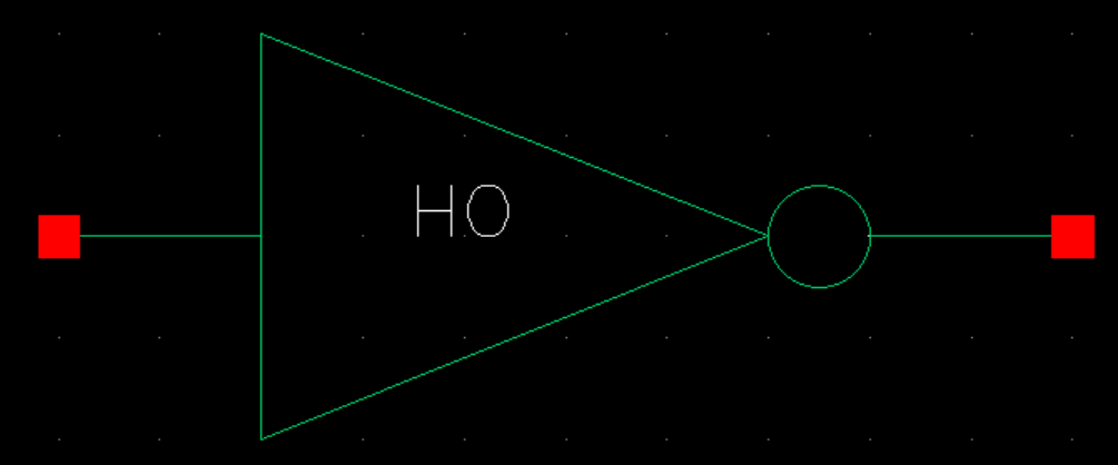
for the invertor. Then create a symbol representing the inverter.
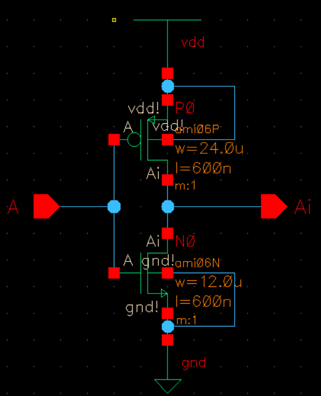
Following this we will create the schematic for the non-inverting buffer circuit. In this schematic we will use the inverter that we
created for both the first inverter and second inverter in the schematic. Also we will set out capacitors as mosfet to make things
easier for when we are doing our layout.
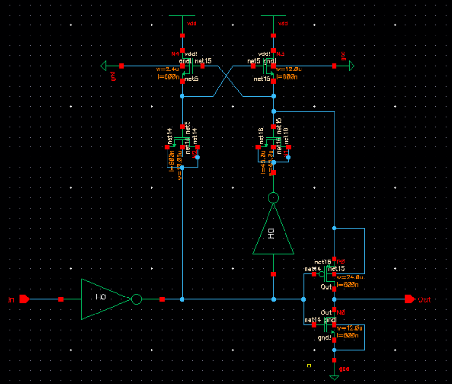
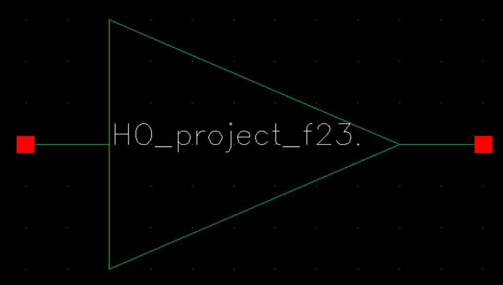
The next thing following our non-inverting buffer schematic is to create a symbol to represent it. Then we will create a simulation
schematic to test the non-inverting buffer.
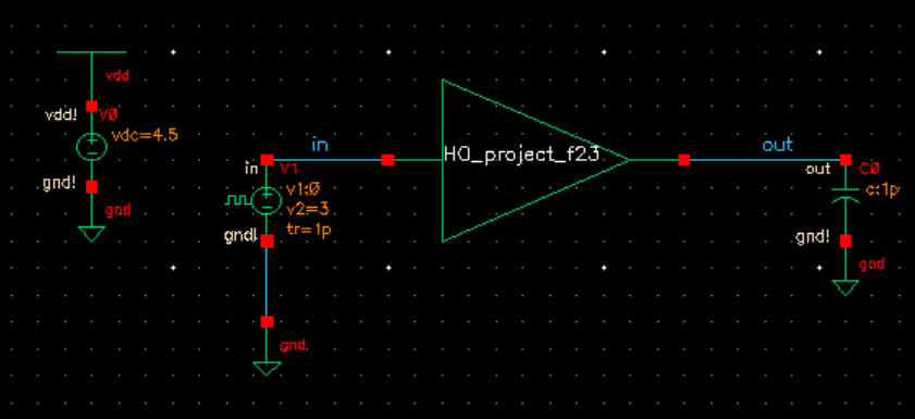
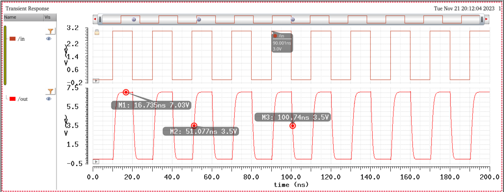
Now, that I have mt sim schematic i will setup the VDD to be 4.5V, the input voltage to be 3V, and with 1pF Cload. Below we can
see the sim results. As we can see the Vin is at 3V. Since the input voltage is 3, it means that the voltage for the output will result
in 2VDD, which should be greater than 7V. As we can see we meet requirement, Vout = 7.03V. The tphl= 1ns and the tplh= 0.7ns.
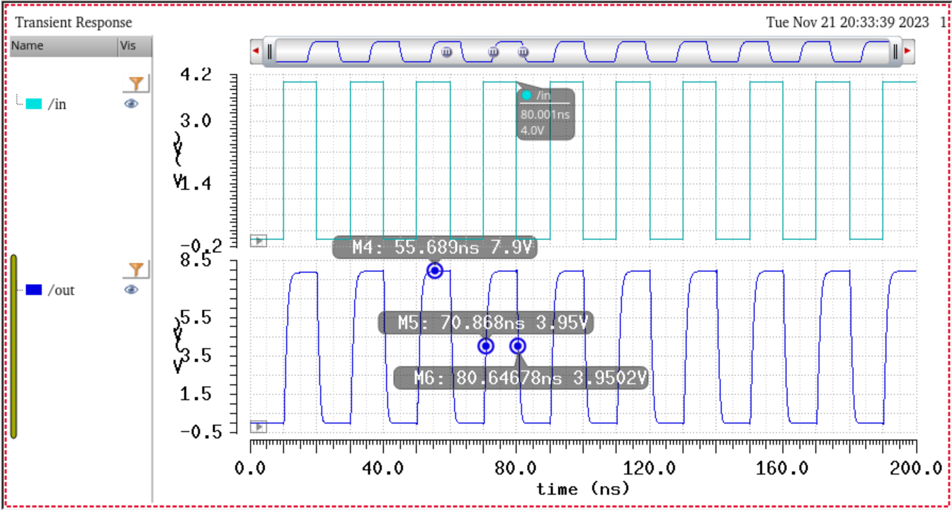
Now, that we got the first example of the simulation we need to test it for multiple cases. The next case will be VDD = 5V, the
Vin = 4V, and the Cload = 1pF. As we can see the we meet the output being greater than 7V, Vout = 7.9V. The tphl= 0.9ns and
the tplh= 0.6ns.
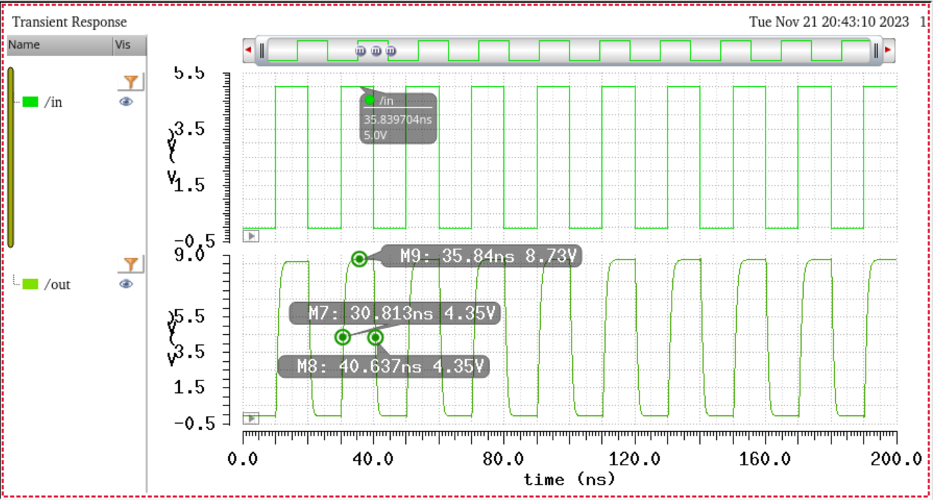
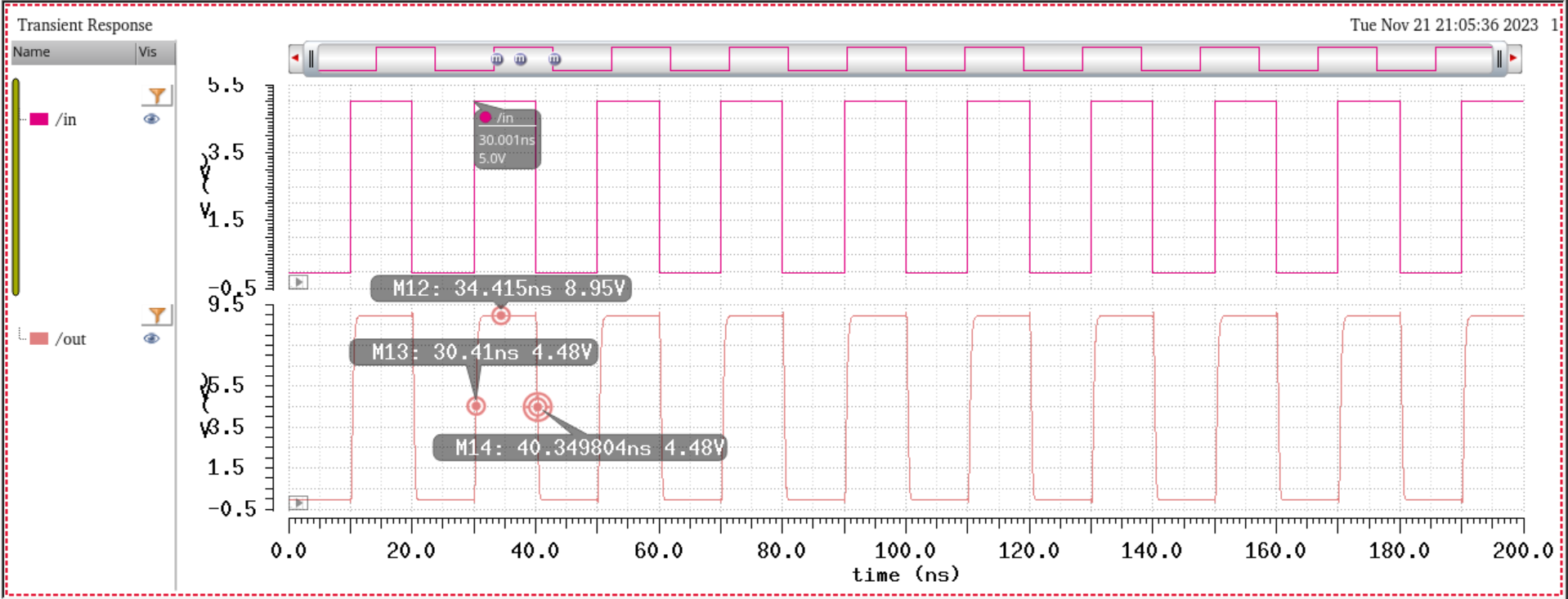
The next simulation we need to test is the VDD = 5.5V, the Vin = 5V, and the Cload = 1pF. As we can see the we meet the output
being greater than 7V, Vout = 8.73V. The tphl= 0.8ns and the tplh= 0.6ns.
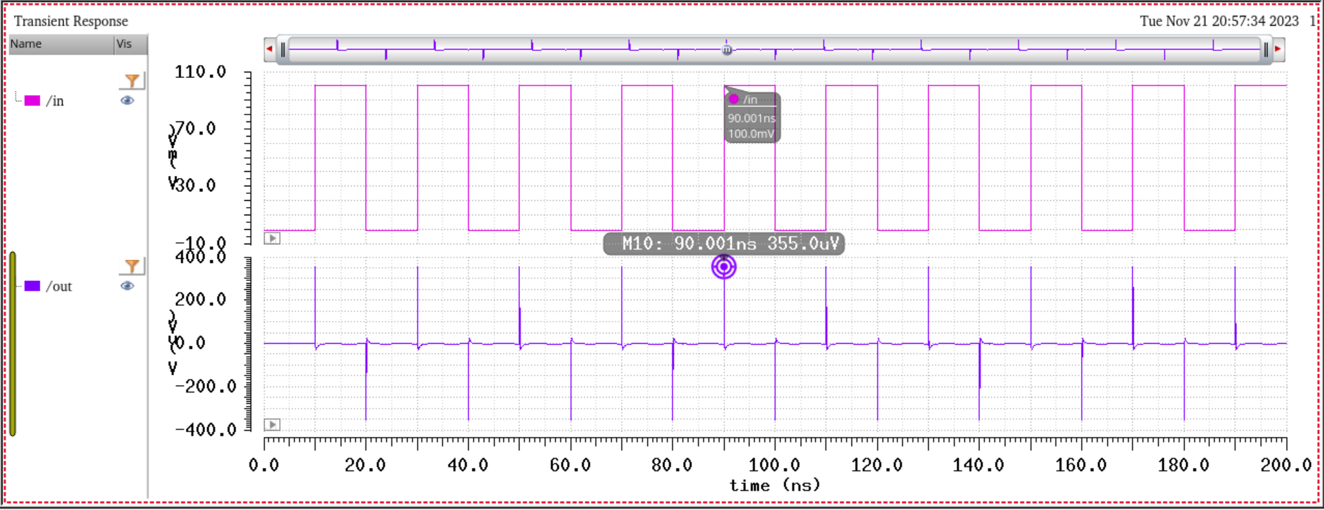
The next simulation we need to test is the logic 0. The way we test this is by setting the input voltage to a value that is less then 1V
I set the VDD = 4.5V, and the Vin = 100mV, and the Cload = 1pF. It can be seen that the output voltage gets 0, since there is
not enough voltage to charge the capacitor, which correlates with the charge-pump clock drive that we discussed earlier.
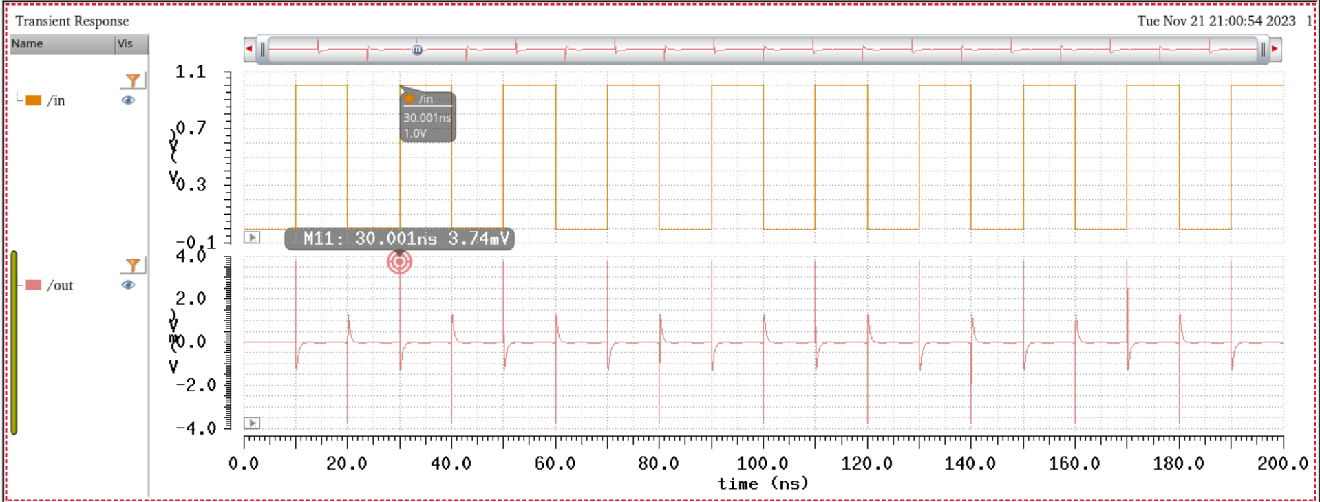
The next simulation will be the logic 0 again. In this case we will set the input voltage to 1V. The reason is because the 1V should
act as logic 0. The setup is to have VDD = 4.5V, the Vin=1V, and the Cload= 1pF. The results will be a 0 as it did in the charge-
pump clock drive in the beginning.
The next thing to simulate will be to check if my design works with varying load capacitances from 0 to 1pF. This simulation will
have the VDD= 5V, the Vin= 5V, and the Cload= 250fF. Now, we see that the Vout= 8.95V, and the tphl= .4ns, as well as the
tplh= 0.3ns.
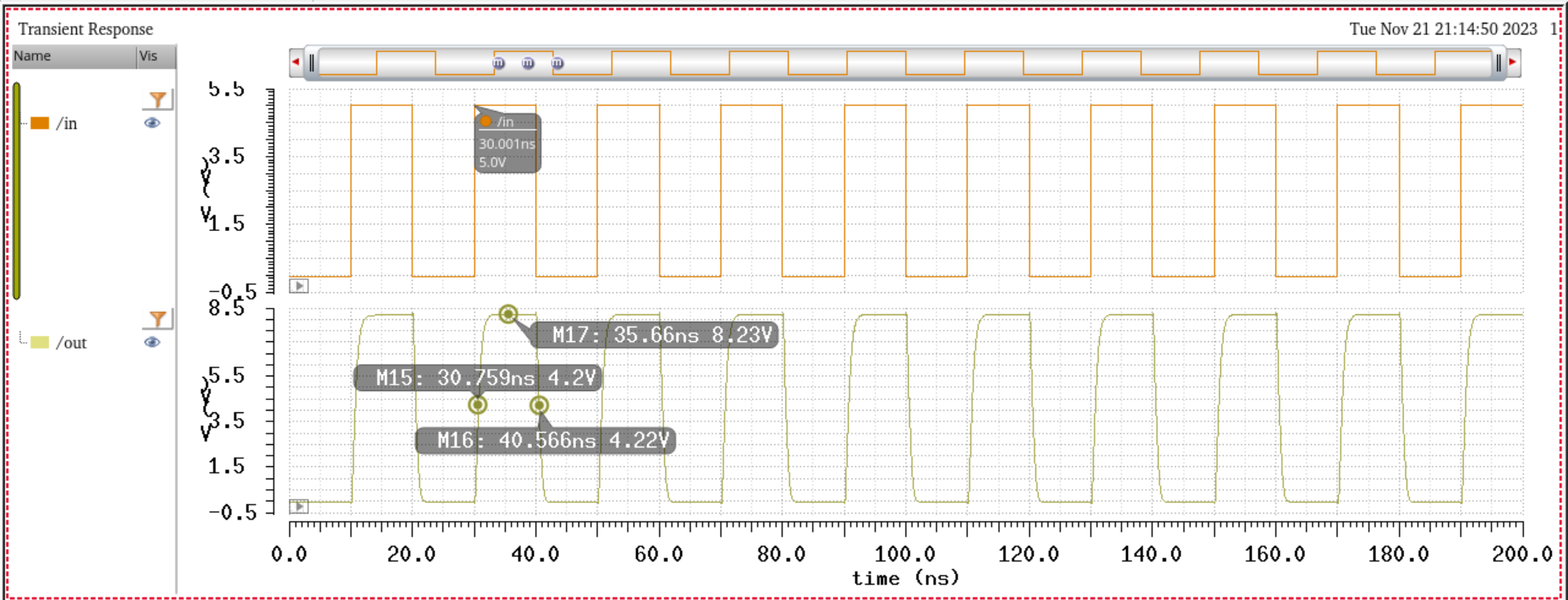
The next simulation we will do for checking the varying load capacitance is by setting the VDD= 5V, Vin= 4V, and finally the
Cload= 750fF. The voltage output being greater than 7V is met. The the Vout = V,tphl= 0.8ns and the tplh= 0.6ns.
Non-inverting Buffer Layout
__________________________________________________
The first thing to do is make the layout for the inverters we will be using. Then to DRC check it, so that we get no errors. When there is no error, then
extract the layout and LVS it so that they match the schematic of the inverter.
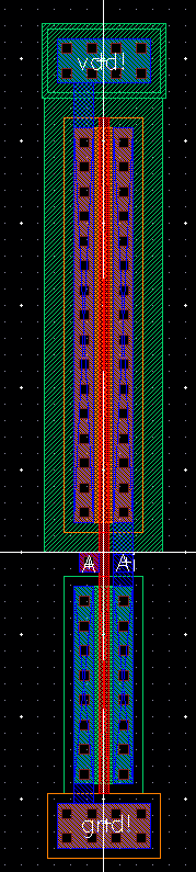
Inverter Layout
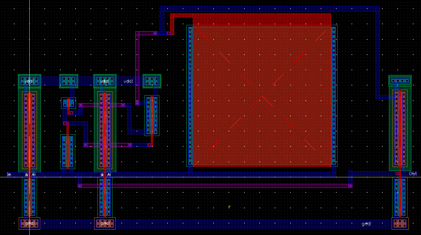
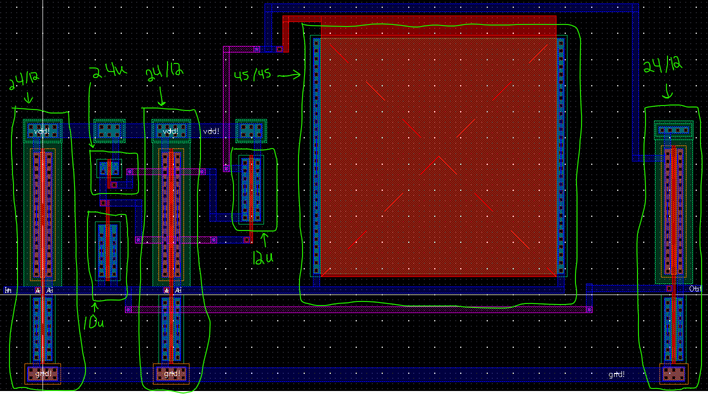
Now that we got the inverter layout, we can begin laying out the whole schematic. Below we can see the whole layout complete. Also,
we can see how the layout matchs the schematic below.
Full Layout
Labeled Layout
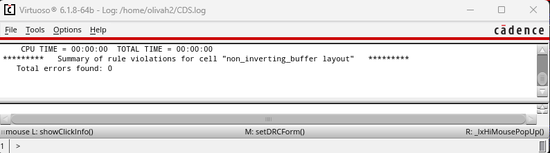
After completeing the layout DRC check it, got zero errors.
DRC
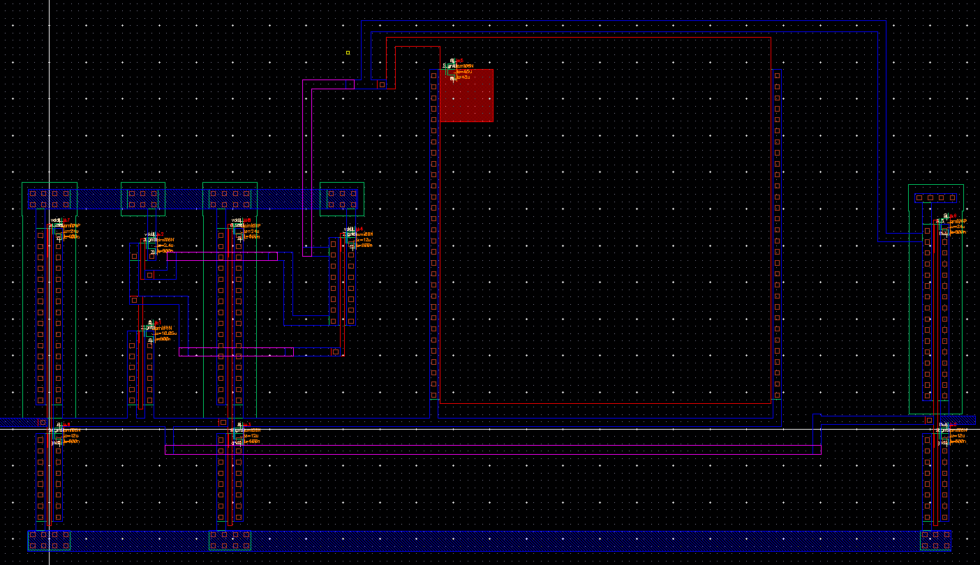
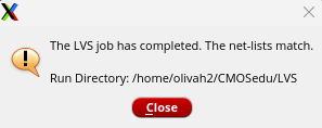
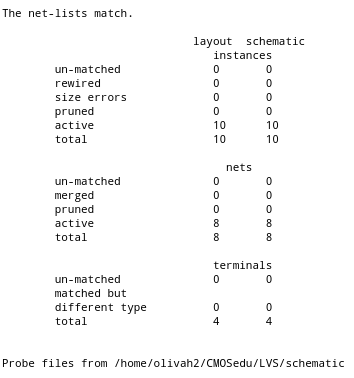
Next, extract the layout. Then LVS check the extracted layout with the schematic and it should match. Layout is finished.
Extracted View
LVS (match)
The project file for this is below.
Return to EE 421L Labs