Lab 4 - ECE 421L
Authored
by Ronnie Moran, moranr1@unlv.nevada.edu
Today's
date: 9/27/23
Prelab:
Here is the NMOS layout view:
Here is the PMOS layout:
Lab work:
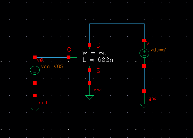
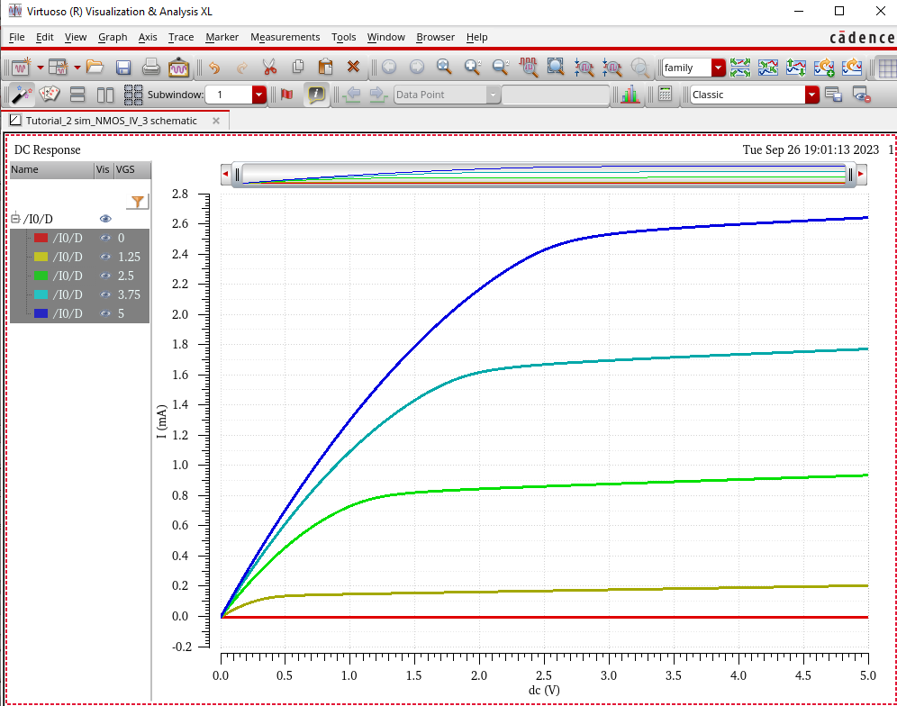
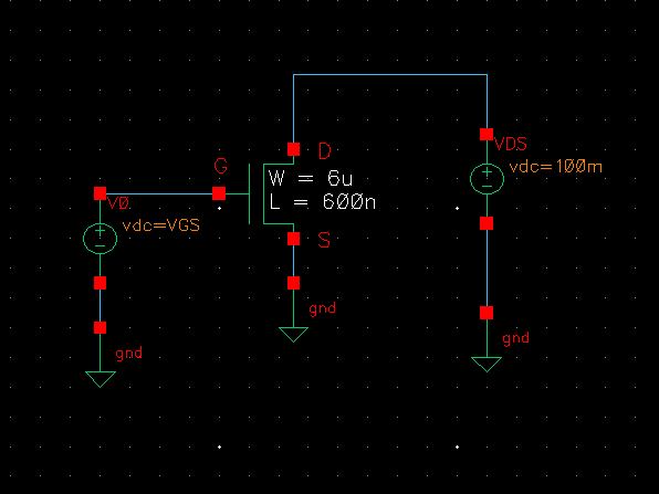
Here is the schematic for ID v. VDS for the NMOS device for VGS varying from 0 to 5V in 1mV steps. Our width and length (W/L) = 6u/600n.
Result:
Here is the schematic ID v. VDS for the NMOS device for VGS varying from 0 to 2V in 1mV steps. Our width and length (W/L) = 6u/600n.
Result:
For this part of the lab it will be fairly similar to the NMOS
portion just with PMOS. We will be making a schematic for ID v. VSD of
a PMOS device and VSG will be varying from 0 to 5V in 1V steps while
VSD varies from 0 to 5V in 1mV steps. Our width and length (W/L) =
12u/600n.
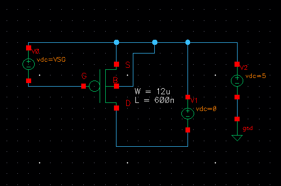
Result:
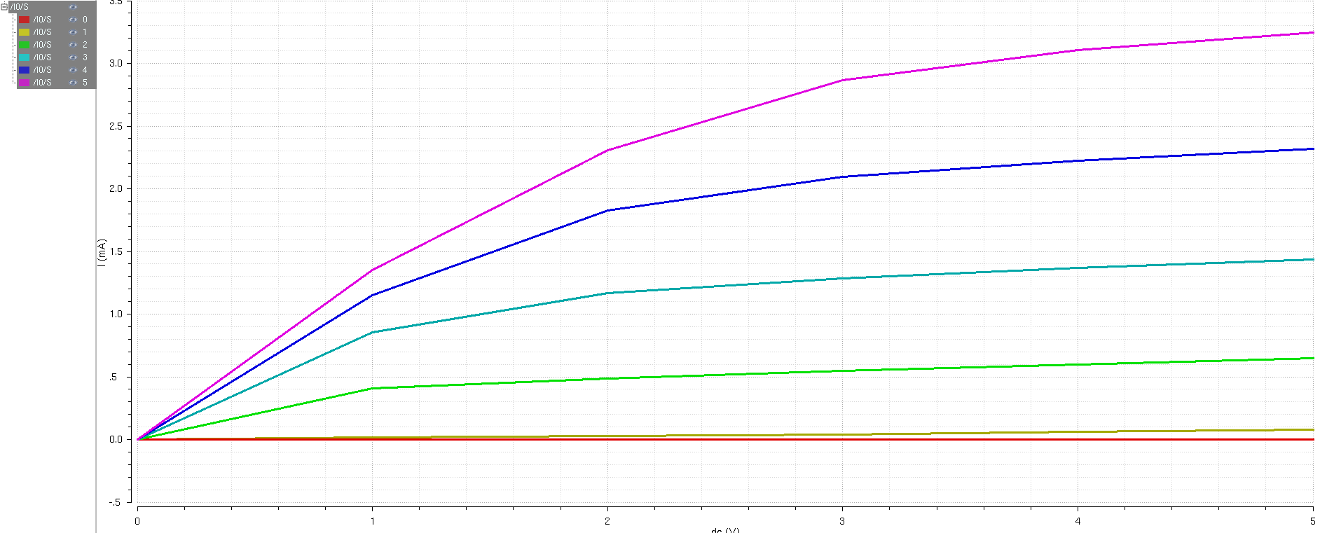
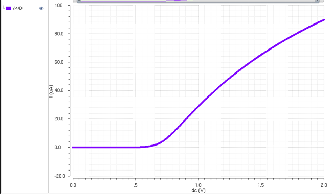
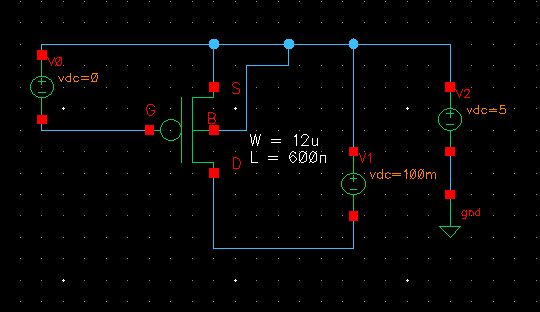
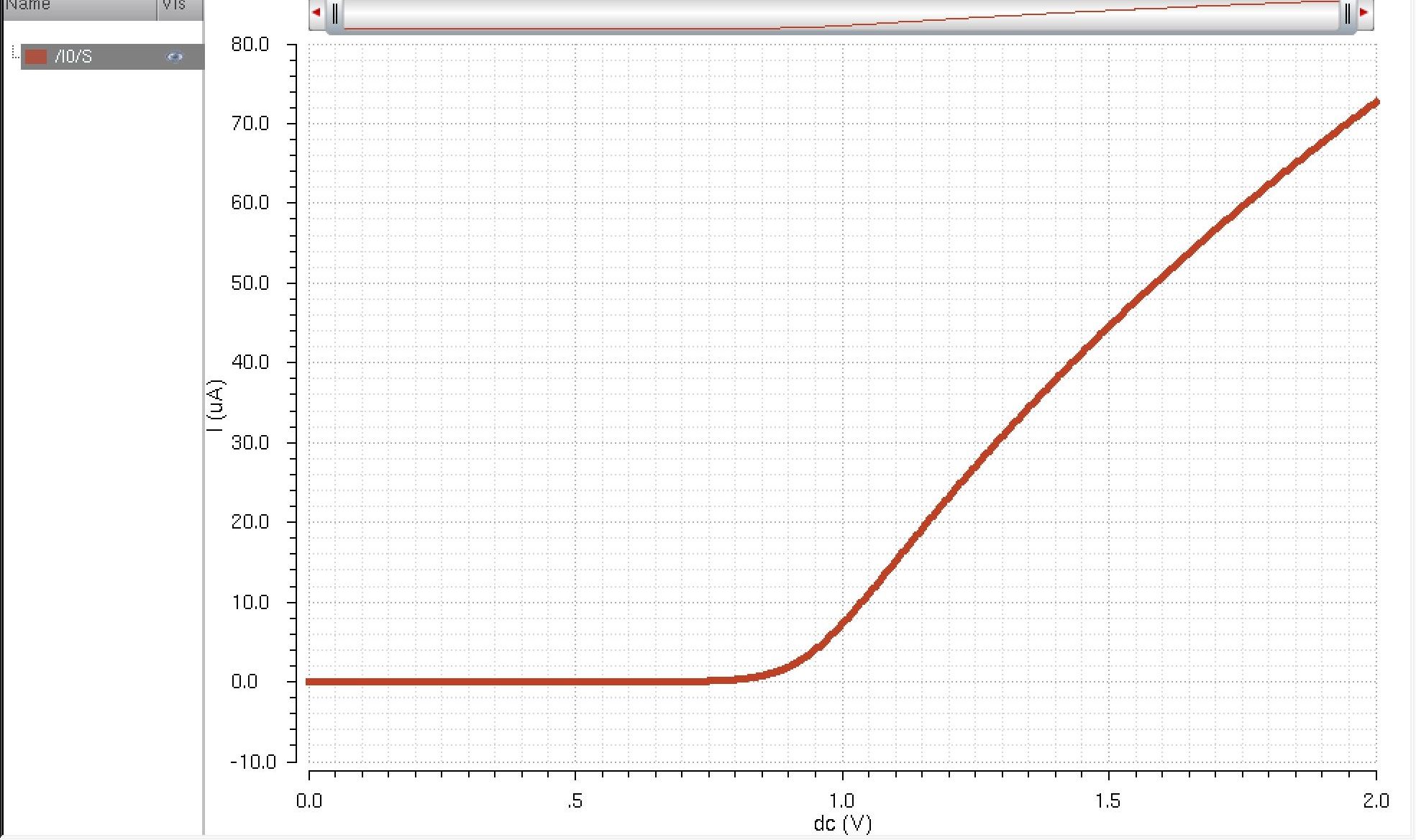
This will be a schematic for ID v. VSG of a PMOS device for VSD = 100mV
where VSG varies from 0 to 2V in 1mV steps. Our width and length (W/L)
= 12u/600n.
Result:
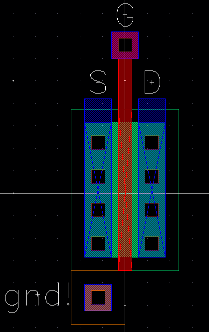
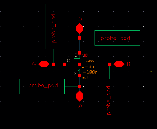
In this part of the lab we will layout a 6u/600n NMOS device and connect all 4 of the MOSFET terminals to probe pads.
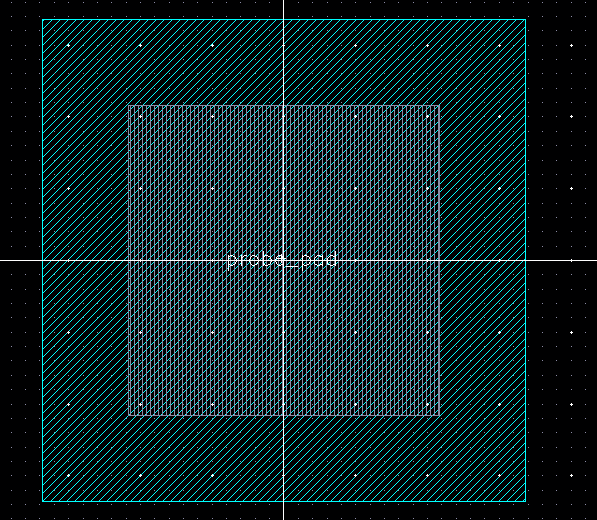
Here is the layout of the probe pab given from the lab4.zip
Here is the layout of the NMOS connected to the probe pads.
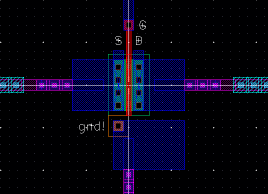
NMOS layout zoomed in:
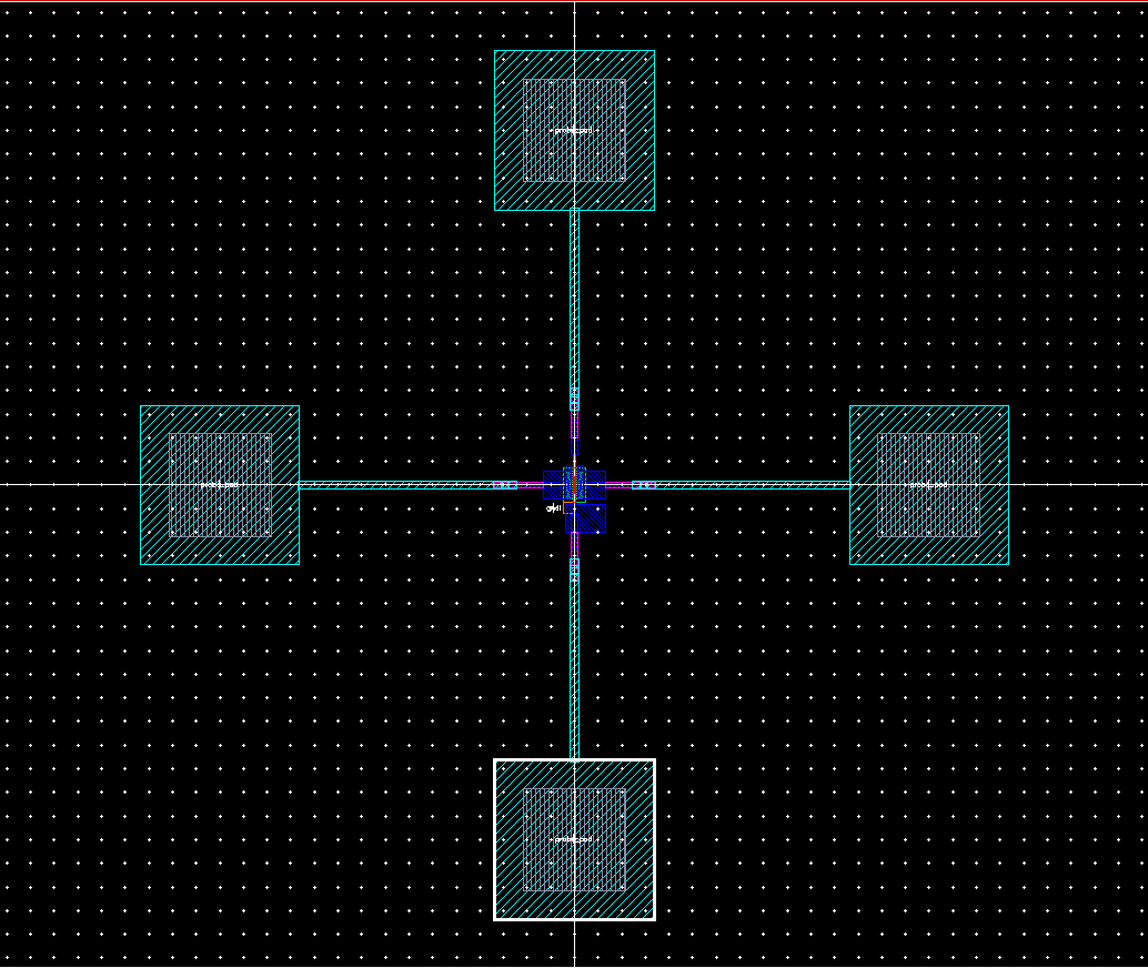
Here is the full layout view of the NMOS:
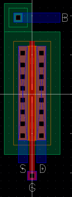
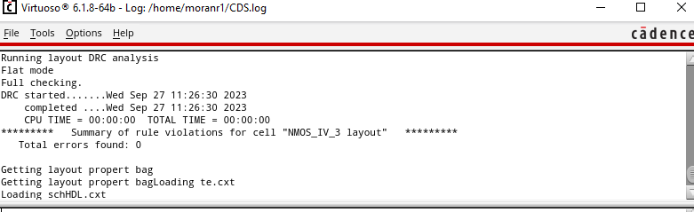
DRC NMOS:
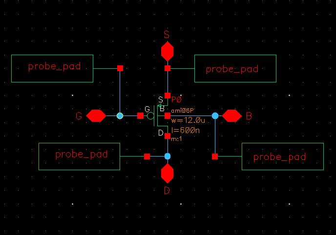
Here is the PMOS connected to the probe pads.
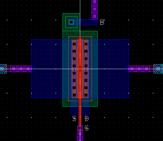
PMOS layout zoomed in:
Here is the full layout of the PMOS

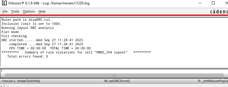
PMOS DRC:
I backed up work shown in the prelab steps.
Return to EE 421 Labs