Lab Project - EE 421L
Authored
by Ronnie Moran, moranr1@unlv.nevada.edu
Today's
date: 11/21/23
Lab Project: Design a non-inverting buffer circuit that presents less than 100 fF input capacitance toon-chip logic and that can drive up to a 1 pF load with output voltages greater than 7V (an output logic 0 is near groundand an output logic 1 is greater than 7V). Assume VDD is between 4.5V and 5.5V, a valid input logic 0 is 1V or less, a valid input logic 1 is 3V or more. Show that your design works with varying load capacitance from 0 to 1 pF. Assume the slowest transition time allowed is 4 ns.
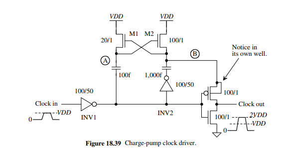
Chapter 18 Book Schematic used as a reference along with lab notes:
Project Work:
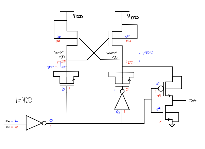
Charge Pump Hand Schematic:
Cadence Schematic:

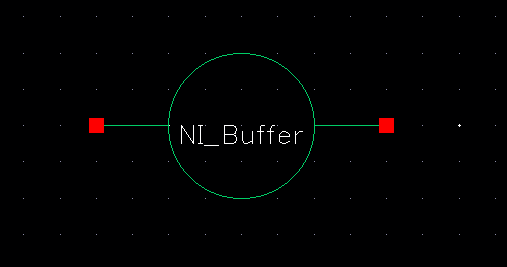
Symbol View of my charge pump:
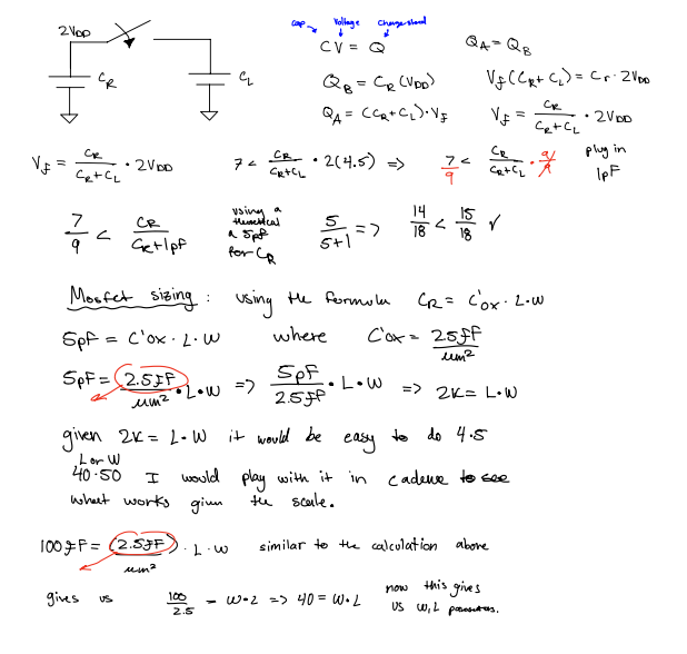
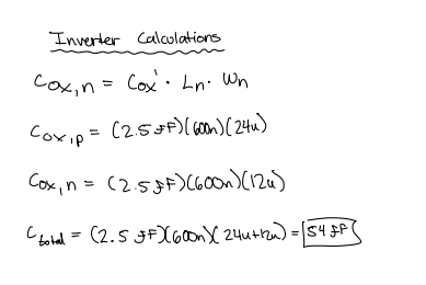
Hand Calculations for the MOSFETs used in the schematic:
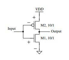
Inverter Schematic:
Project Simulations:
The
first simulation is to test how varying VDD from 4.5,5,5.5V affects
Vout (labeled out) in the simulations along with our transitions times.
We have no load in this simulation.
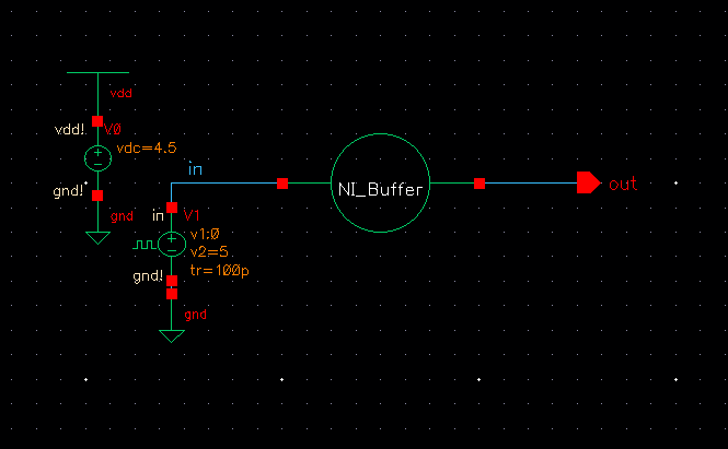
The
schematic is the same besides changing the VDD value so I will not be
showing that change but I am noting it verbally in my report to clarify.
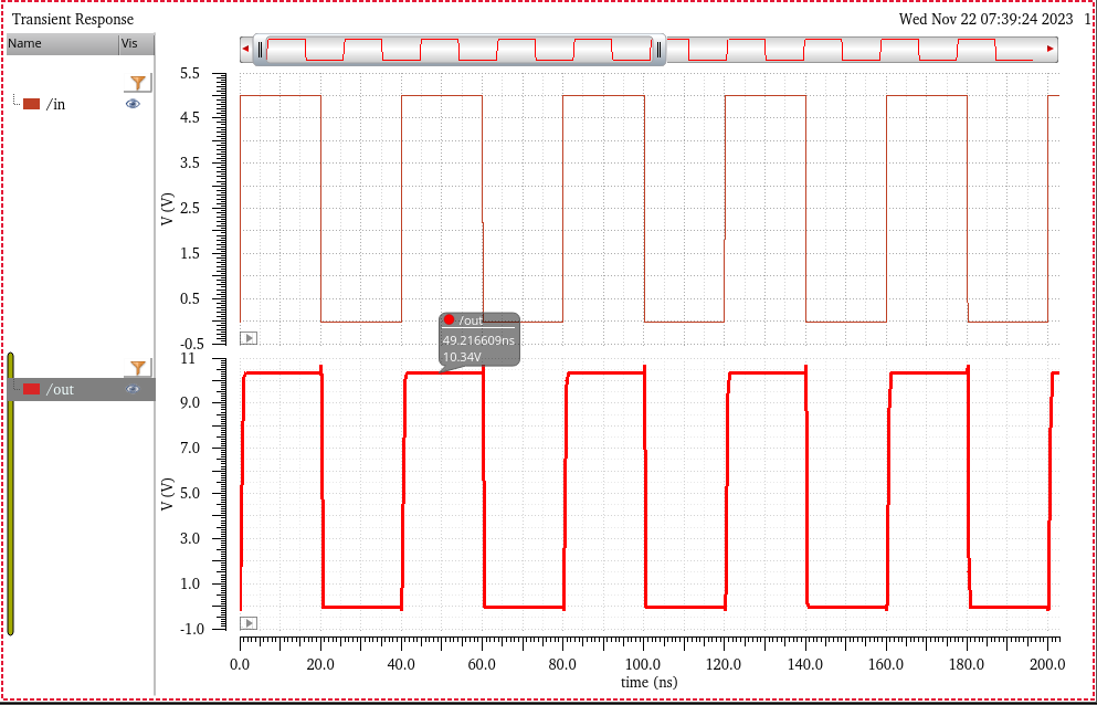
VDD @ 4.5V
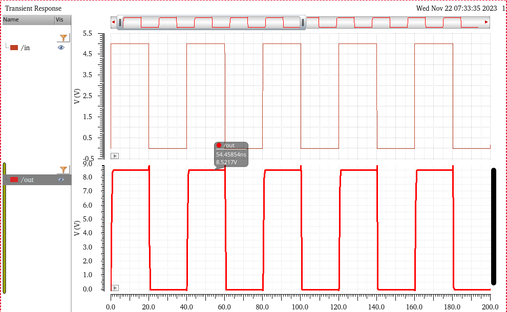
VDD @ 5V
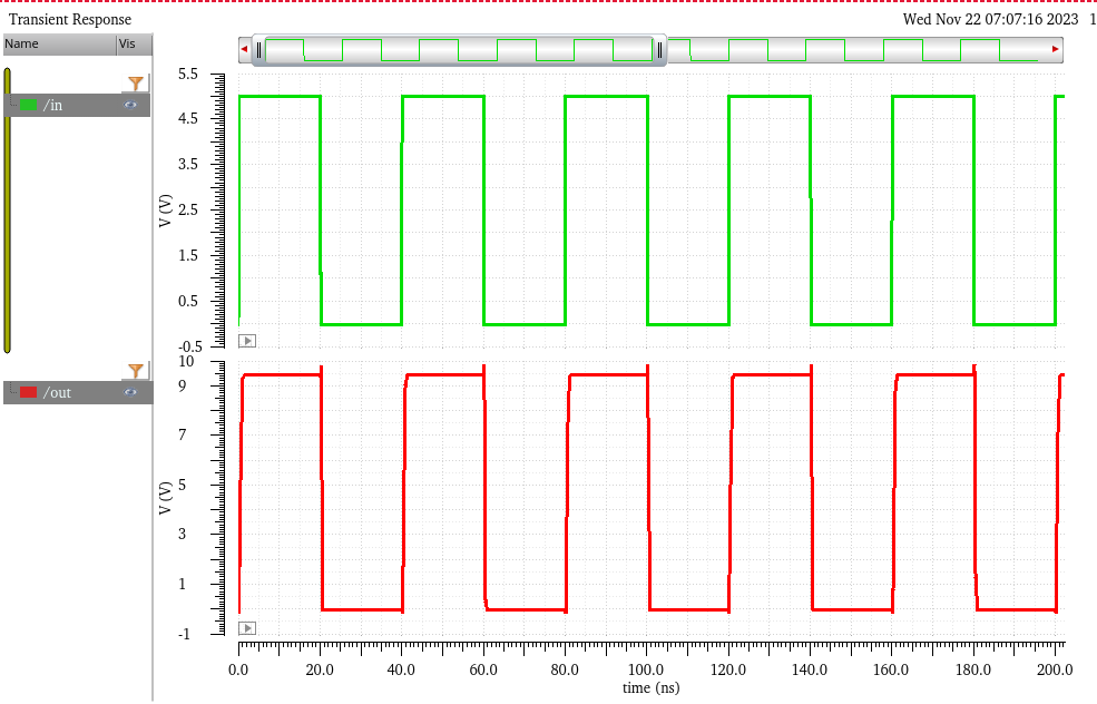
VDD @ 5.5V
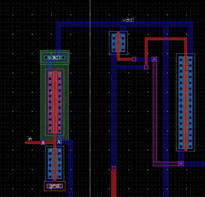
Layout:
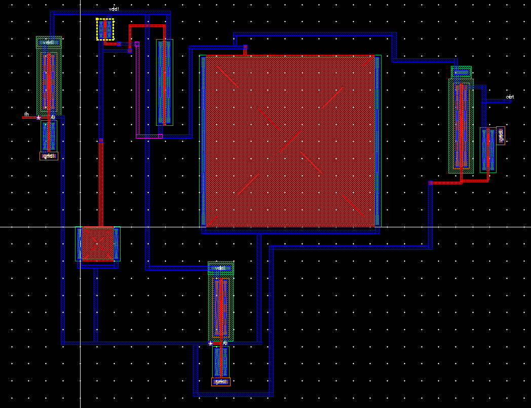
Close ups for pins:

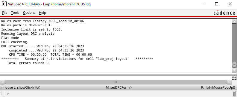
DRC stands for Design Rule Check to essentially confirm there aren't
any issues with the layout. Components are all grid and or too close to
each other during that layout process. As the screenshot below shows my
layout passes with no errors:
LVS stands for Layout versus Schematic. It a confirmation that our
layout we completed in Cadence matches the circuit schematic shown
above are a match for each other. I was not able to get my layout to match my schematic.
On top of starting late, I was not able to get the si.out or si.log to
display the message correctly. I was not able to debug the layout in
order to get a proper LVS message in the end. At least I did not fake
the screenshot.
Return to EE 421 Labs