Lab 6 - ECE 421L
Authored
by Ronnie Moran, moranr1@unlv.nevada.edu
Today's
date: 10/28/23
Prelab:
The Prelab work this lab was to follow tutorial 4 and show our results.
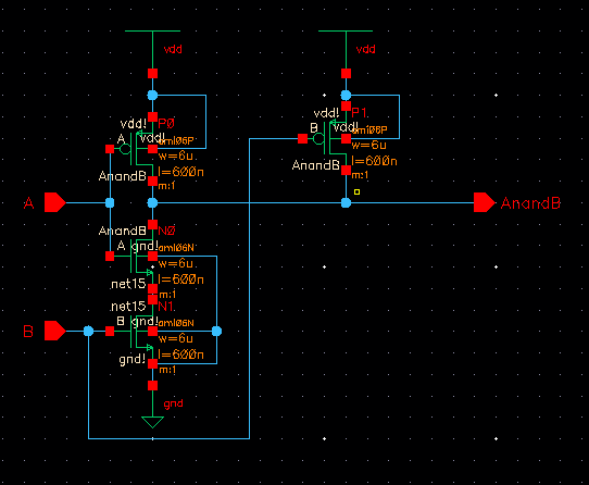
Here is my schematic of my NAND gate:
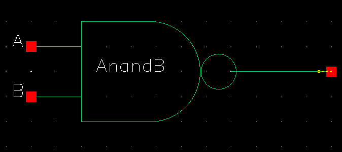
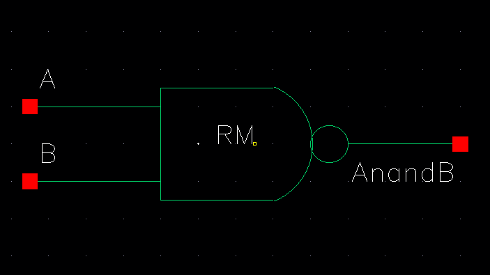
Symbol View:
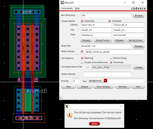
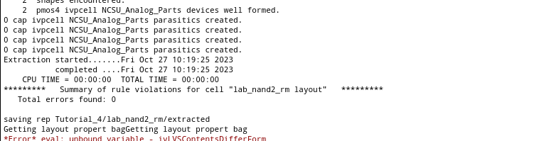
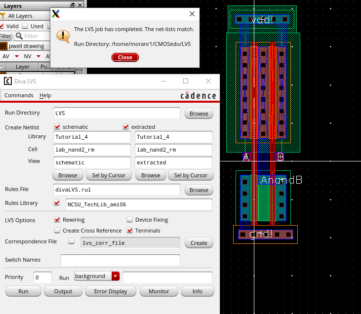
Layout with DRC/LVS:
Lab Work:
In this lab we will be designing a NAND gate, XOR gate, and a Full adder.
This means each design will have a corresponding symbol, layout, and simulations.
1. NAND Gate:
Here is my schematic for the NAND gate which I will make a symbol from this cellview.
Symbol View:
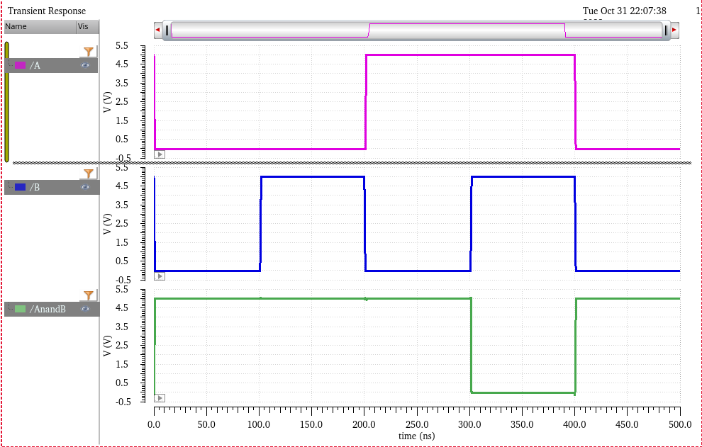
Simulation of the NAND gate:
Layout with DRC/LVS of the nand gate similar to the one in the prelab nut not quite:
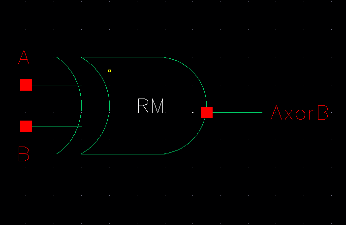
2. XOR Gate:
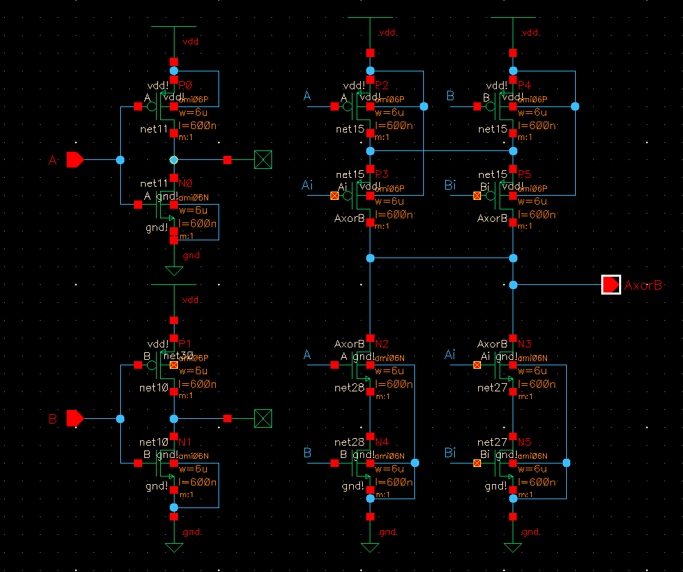
Here is my schematic for the XOR gate which I will make a symbol from this cellview.
Here is the symbol view:
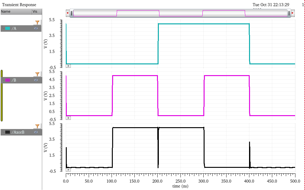
Simulation of the XOR gate:
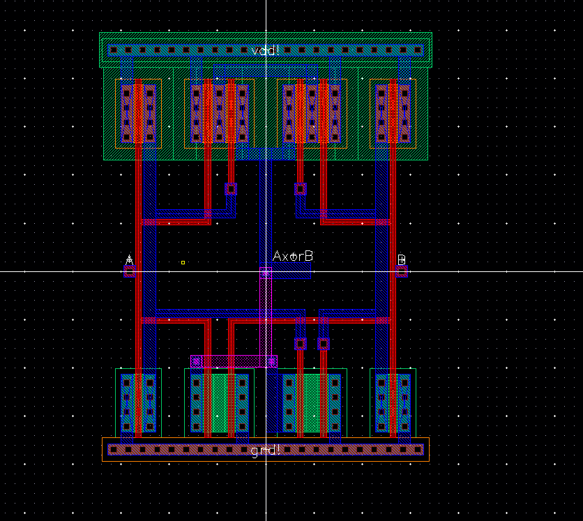
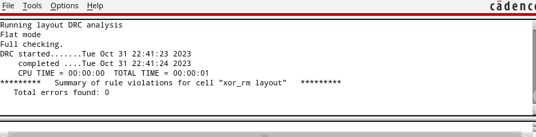
Here is the layout of my XOR gate with LVS/DRC
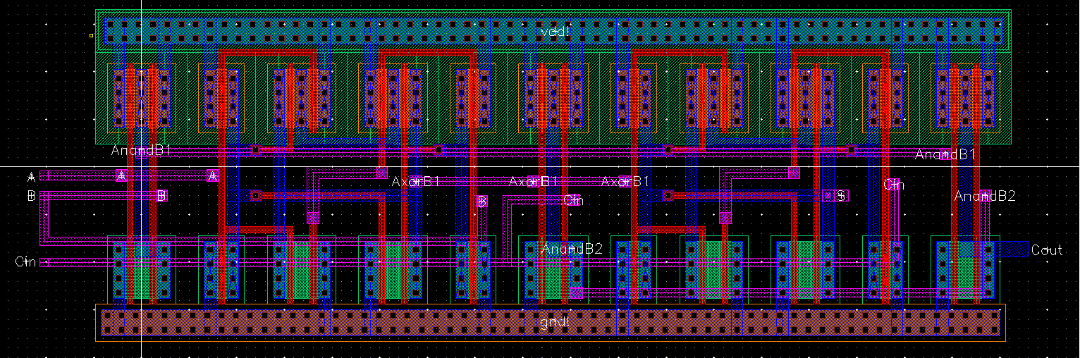
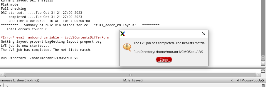
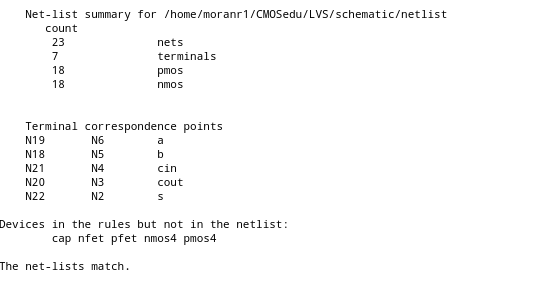
3. Full-Adder:
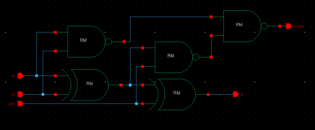
Here is my schematic for the Full-Adder:
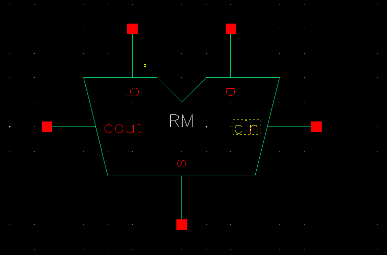
Here is my symbol for the Full-Adder
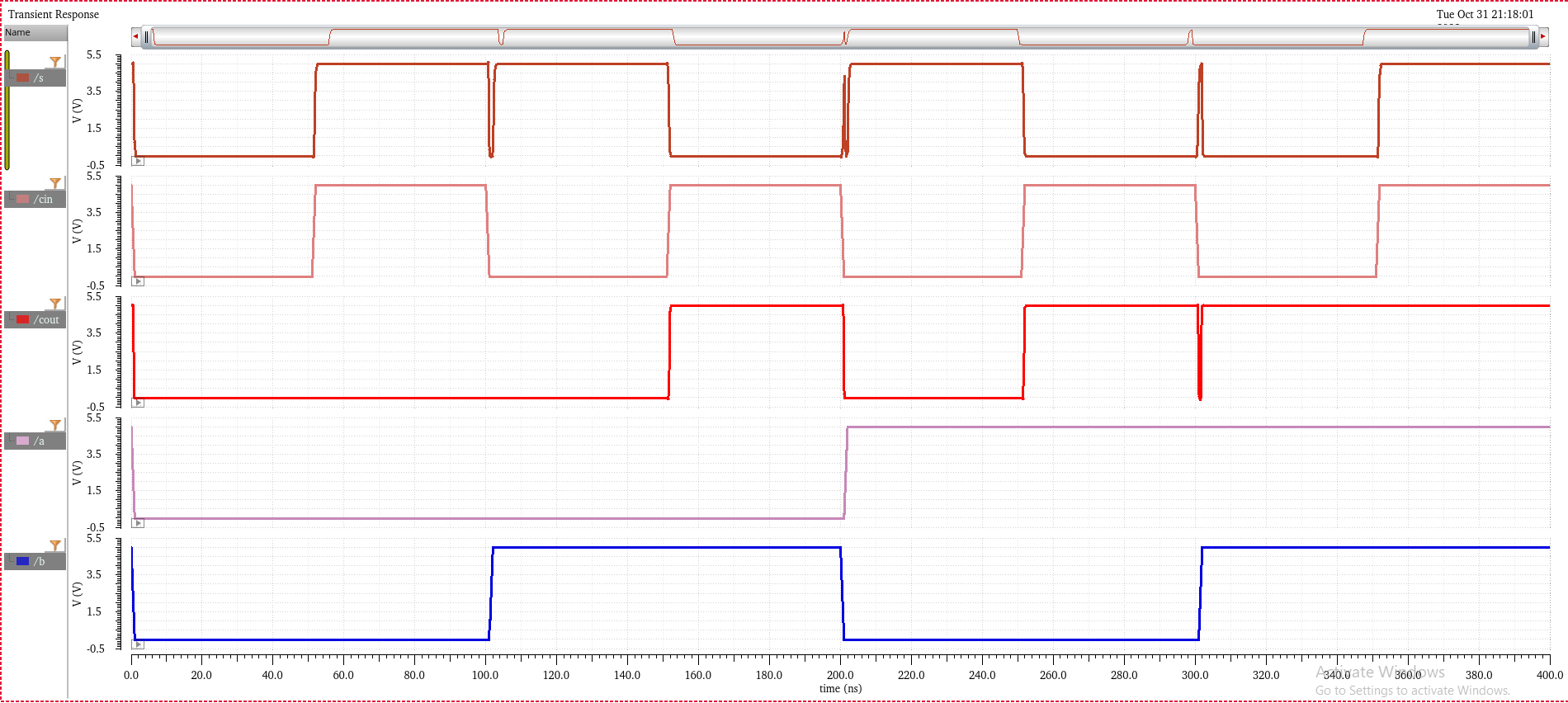
Simulation of the Full-Adder:
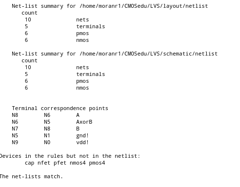
Here is the layout of my Full-Adder with LVS/DRC
Return to EE 421 Labs