Lab Final Project - ECE 421L
Authored
by Benjamin Molina, molinb1@unlv.nevada.edu
Project Description:
We
were asked to design a non-inverting buffer circuit that presented less
then 100fF of input capacitence to on chip logic. The design needed to
drive the output to at least 7V to represent a logic value of "1" and
less then 1V for a logic value of "0". The value of Vdd in this cicuit
could go as low as 4.5V and as high as 5.5V. For the input logic, the
value of a "0" input needed to be 1V or lower while a "1" input logic
needed to be 3V or higher. Finally the design needed to be able to
handle up to a 1pF load capacitence which still being above 7V and have
a transition time of less than 4ns.
Design Process:
To
start I looked at the book for the various types of non-invertig
buffers that can be designed. We were told to reference mostly off of
Chapter 18 for this circuit, more specifically the charge-pump clock
driver circuit.
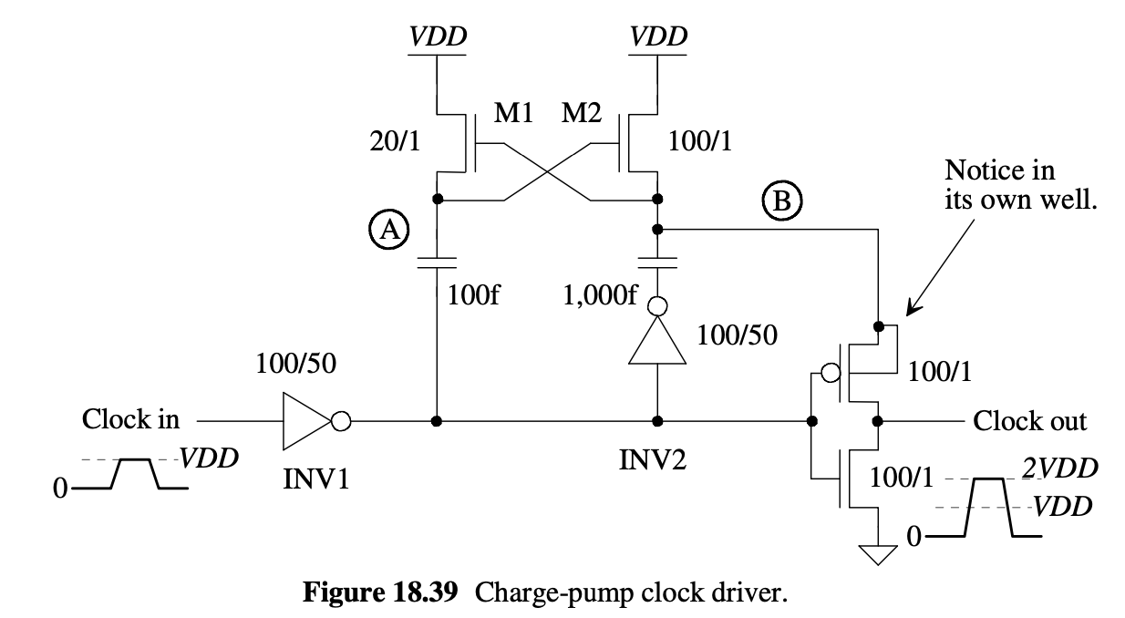
What
then needed to be done was determining the sizes the of MOSFETs that
were going to be used and how big the capacitences for the center part
of the circuit should be. Which can be determined by condensing the
equation and plugging in the load capacitance of 1pF and Vout voltage
of 7V.
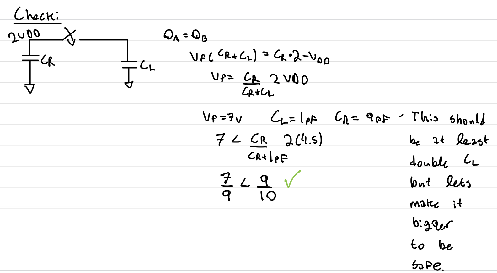
It
was advised that we should make CR at least double the value in order
to get the desired value of 7V. Here we use 4.5 for VDD since it is the
worst case scenerio and makes the fraction of 7/9 a bit harder to deal
with. We need a number for CR to get a bigger fraction on the right
hand side of th inequality. Now we could simply use the bare minimum
number which if we do the math would be 3.5pF to give us exactly 7V.
But designing circuits to meet the limits is not smart. Just to be safe
i used a value of 9pF which gives us a ratio of 9/10 which is bigger
than 7/9 and therefore bigger than all possible fractions we would get
for the VDD range we are given.
Next
the input capacitance for the first inverter needed to be determined.
At first I used the W's and L's found in the book scaled by the C5
Process giving us a 60u/30u ratio for the inverter, but that gave a
capacitance that was too high at around 202fF. Thus I chose to go for the more commonly used values of 24u/12u.
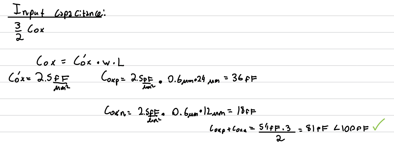
Here we get around 81fF of input capacitance and it falls uder the limit given.
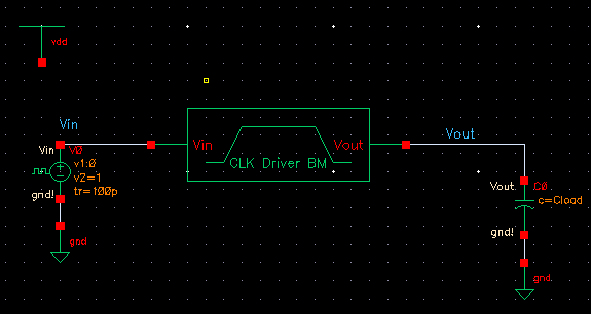
Design:
With the information above the following circuit was designed.
Originally
I used the books W's and L's for the sizes but since the input
inverter's size was scale down I did the same to the other transistors.
Since I sized down the inverter by a factor of 2.5 I chose to do the
same to the rest of the transistors. Given the value seen below.
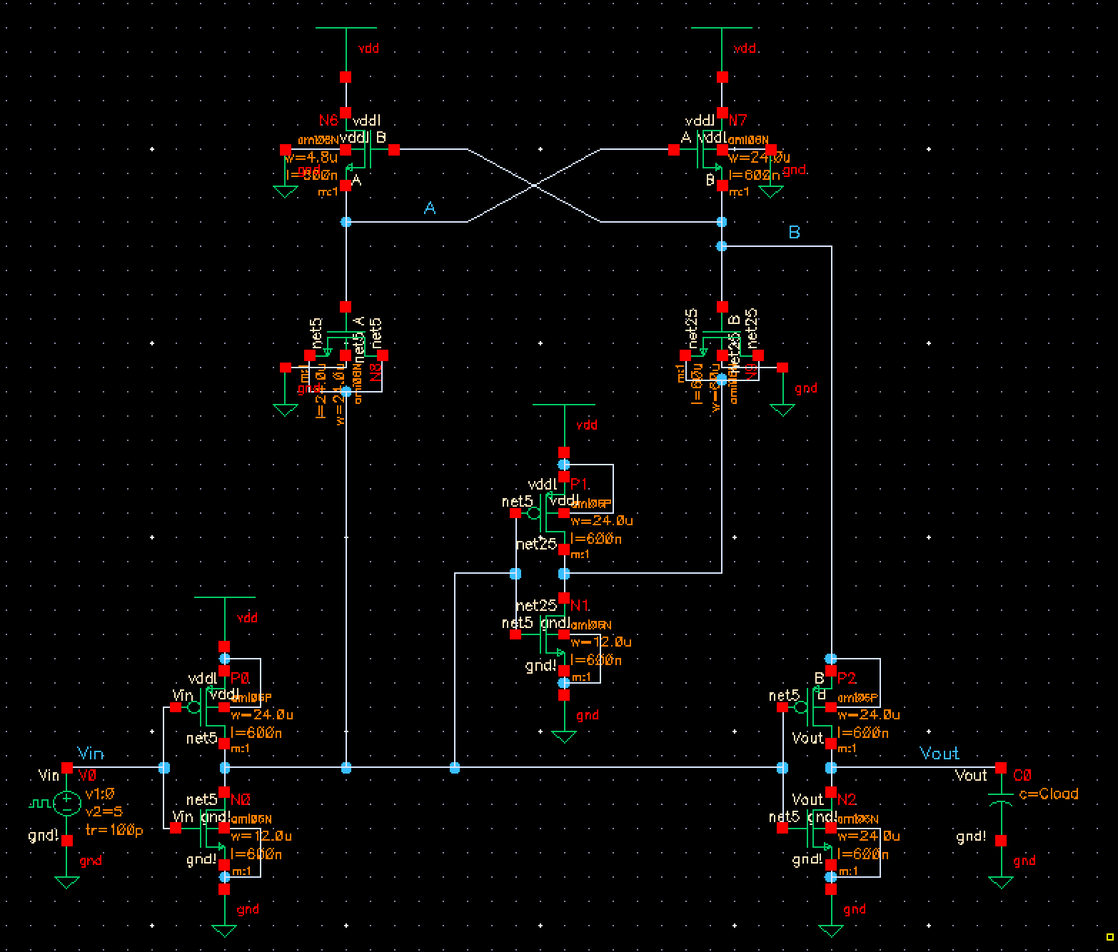
Here
MOSFETs are used as capacitors. This can be done due to the process of
Strong Inversion that MOSFETs are capable of. Essentially VGS of the
MOSFET must be far greater then the threshold voltage Vth. In this
circuit Vdd is VGS and is always far above Vth since we always have at
least 4.5V which is far greater then Vth at 0.7V. All we need to do to
ensure that the MOSFETs act as capacitors is tie Gate, Source and Body
together at one node while gate attaches elsewhere. The following
calculations show the value of capacitors used.
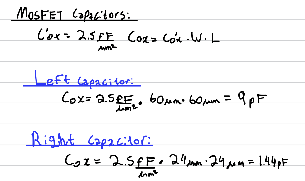
The
left capacitor was chosen to be at 1.44pF inorder to drive node A
higher to be as close to 2VDD at its high point as possible.
Essentially node A and B fluctuate between 2VDD and VDD but are
inverted from each other. Just as making the right capacitor made the
output voltage go higher for our earlier calculations the same will
happen for nodes A and B but one must be careful, making them too high
causes problems in the waveforms. Node A does not give power to the
circuit and this is why the NMOS at the top left corner of the circuit
is smaller than the right one.
Simulations:
In
order to make the simulations I created a symbol for convenience. All
that needed to be done was add pins in the appropriate locations.
| Schematic | Symbol |
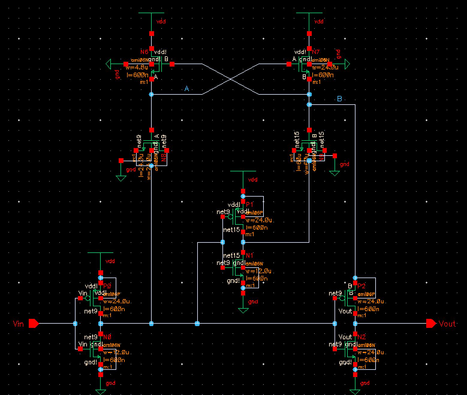 | 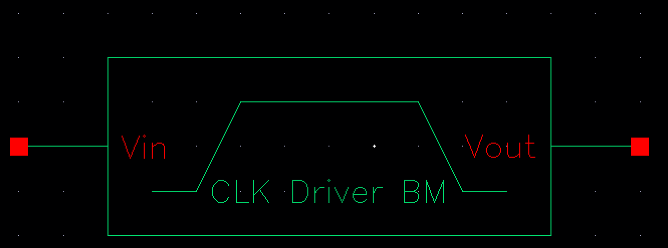 |
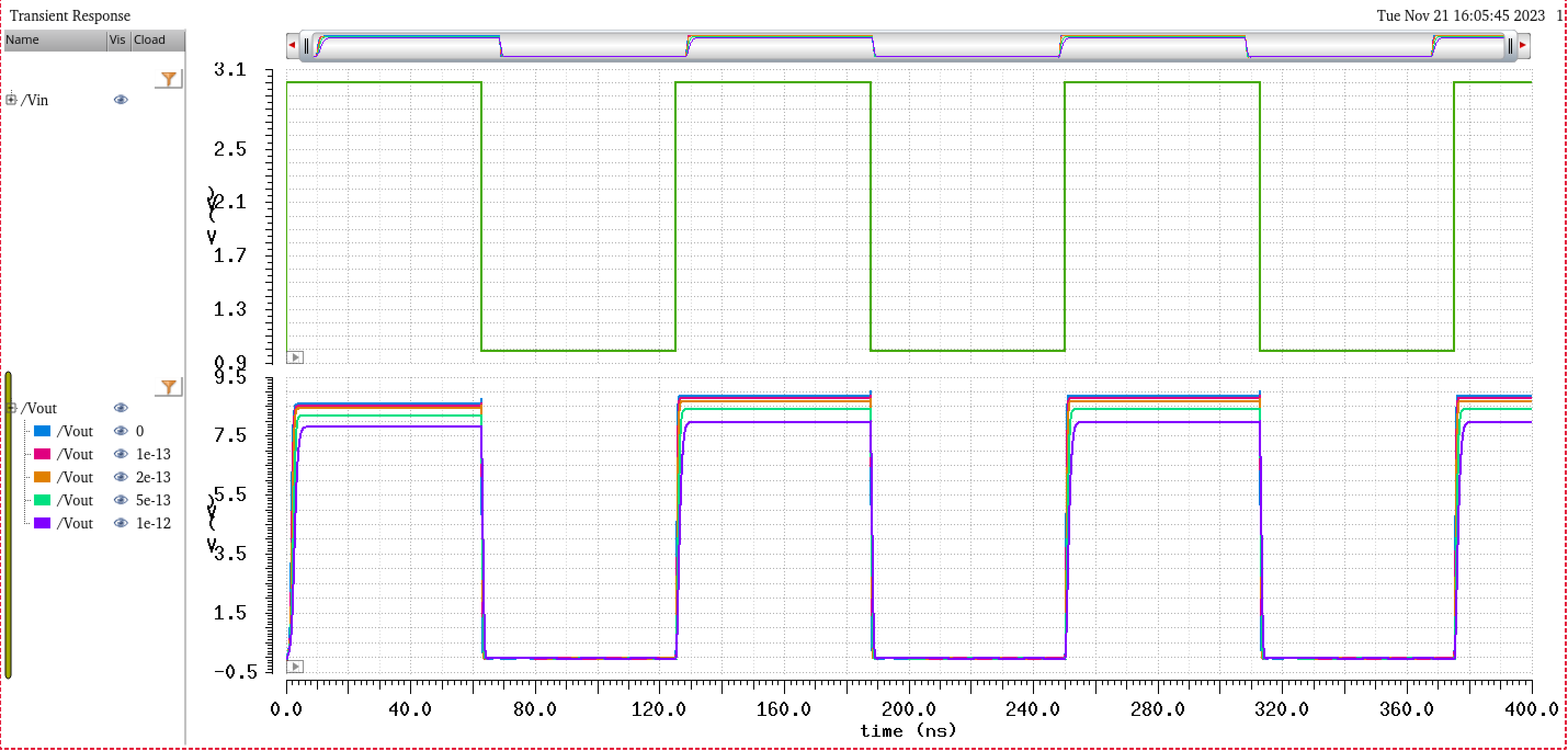
For
effienciency parametric analysis was done to test multiple load
capacitances at once. The capcitances chosen were: 0 100f 250f 500f and
1p. As a result we get the following:
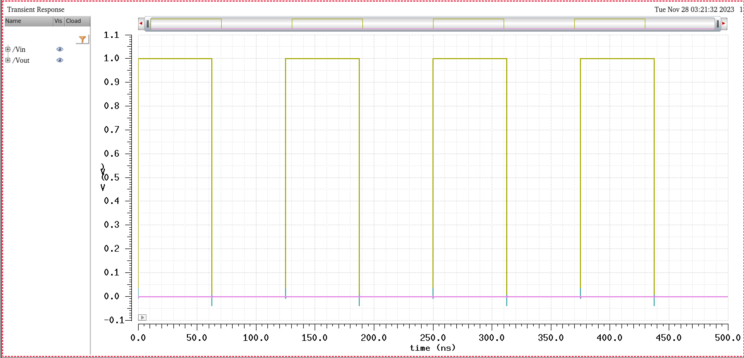
The
circuit needs to identify 1V or lower as a input "0" logic and identify
3V as an input logic "1". In the above table we can see the pulse goes
from 1V to 3V. So here we show what happens when our pulse is 0V-1V
just to be sure:
Where as if we simulate it with a regularly used 0V-5V pulse:
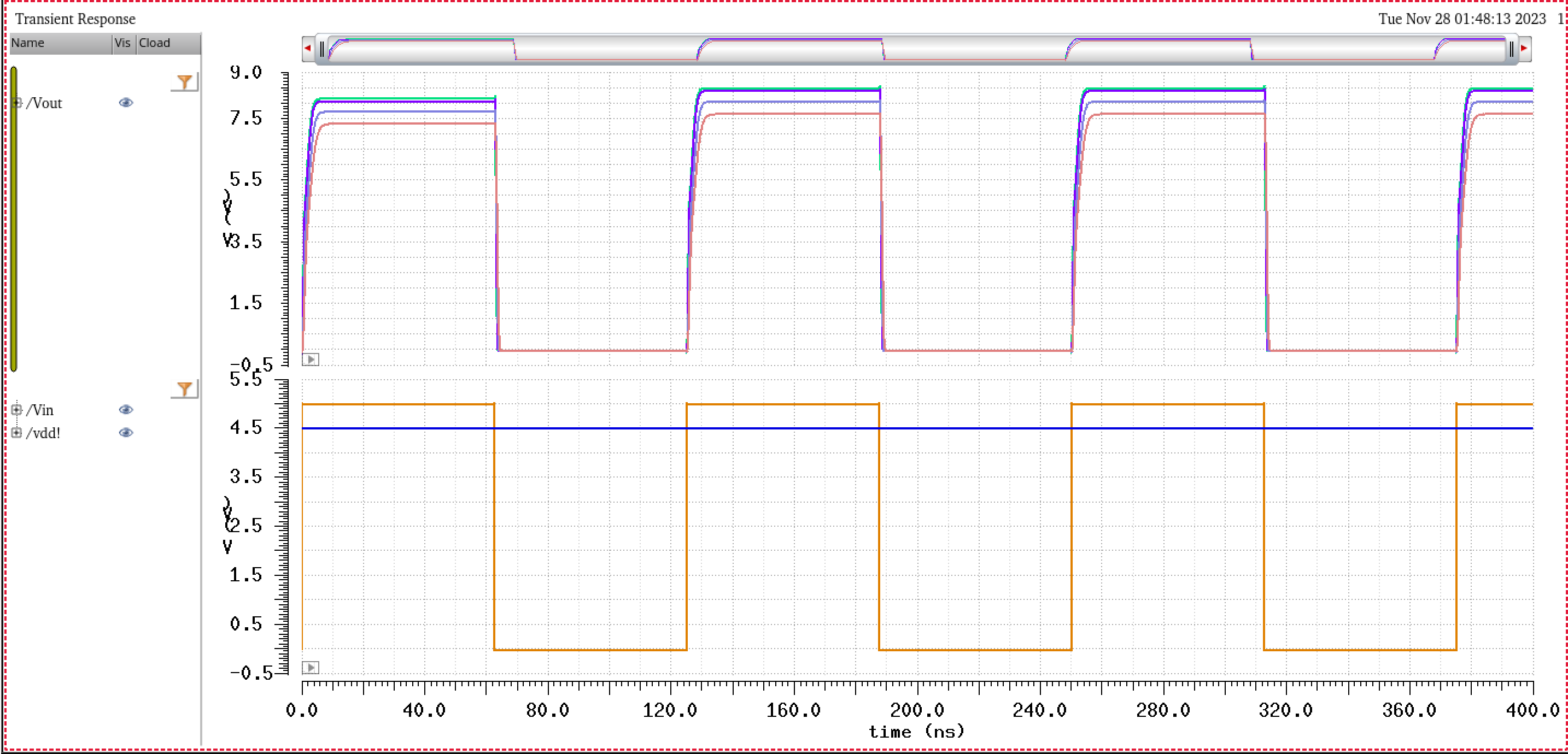
The remaining simulations are done using 0V-5V for convenience.
| VDD | Simulation with 1pF Load |
| 4.5V | 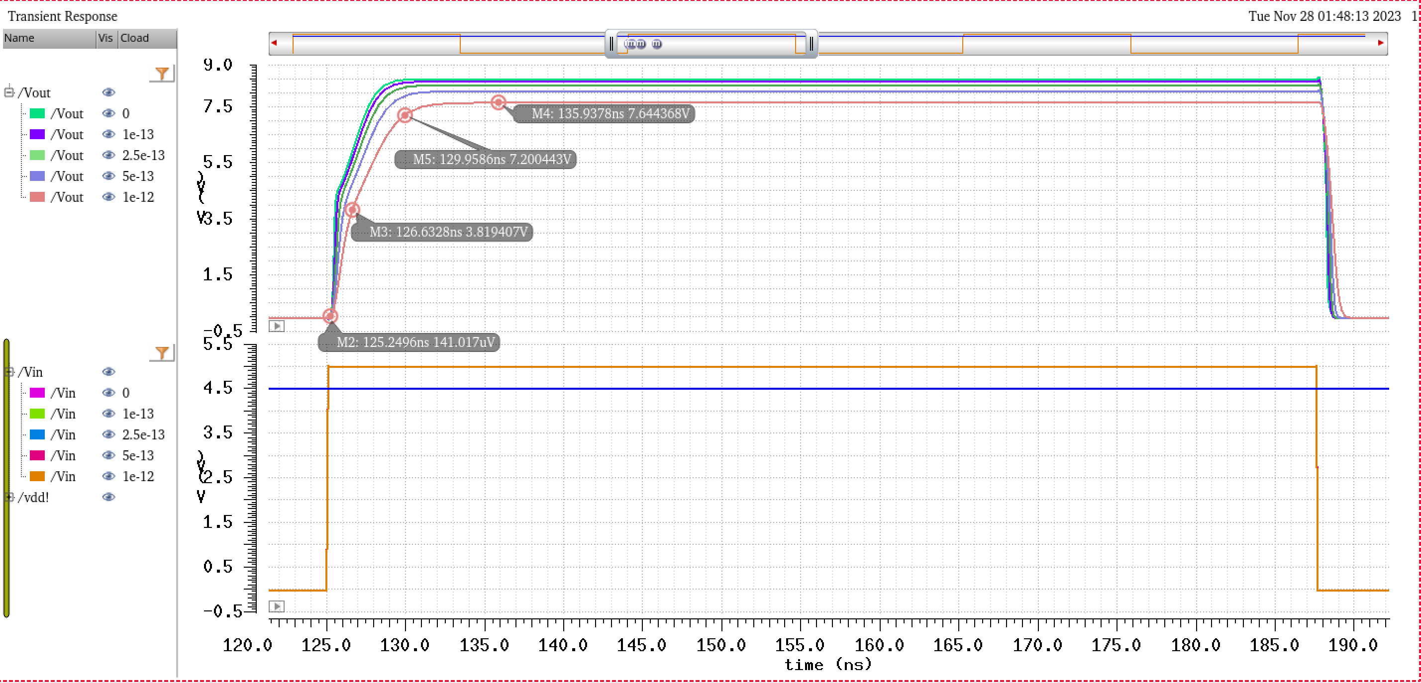 |
| 5V | 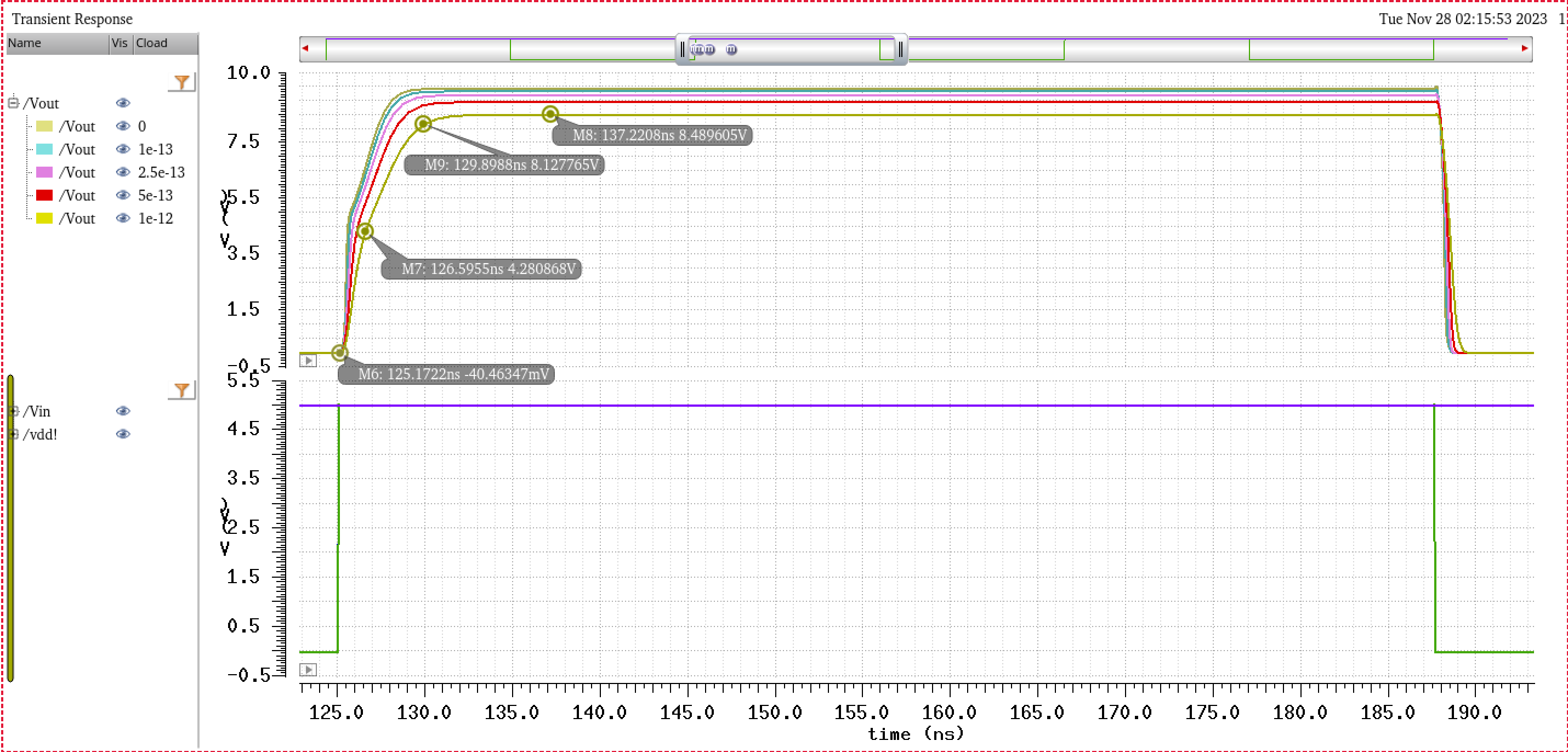 |
| 5.5V | 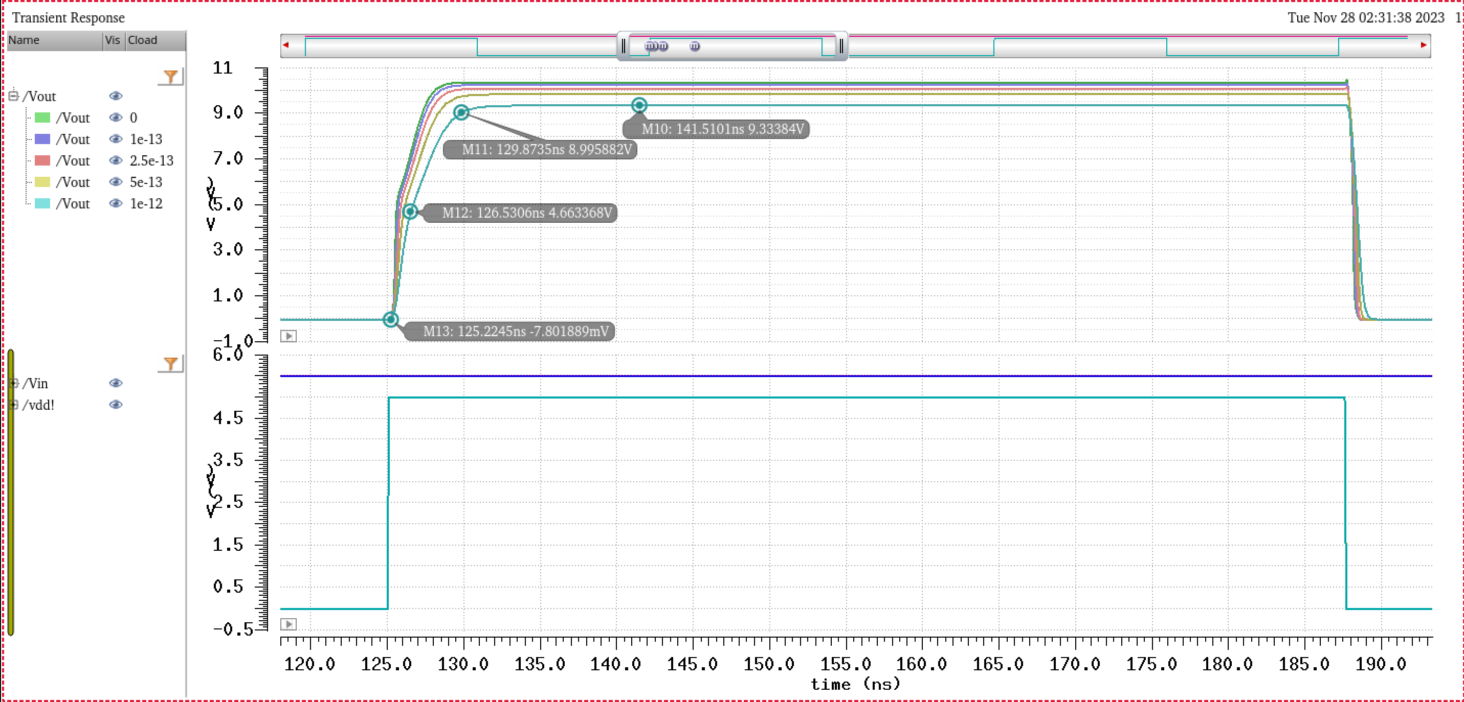 |
As we need to show our dealys are less than 4ns the following calculations were done:
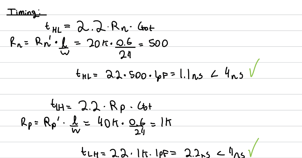
This
along with the simulations indicate a reasonable delay under 4ns of
transition time. These calculated numbers are not actually a perfect
match as seen in the simaultions but it offers a reasonable estimate
under 4ns.
Finally the
following simulation shows all important nodes on the schematic to show
how it should behave. This simulation is done at Vin = 0V-5V and VDD =
4.5V
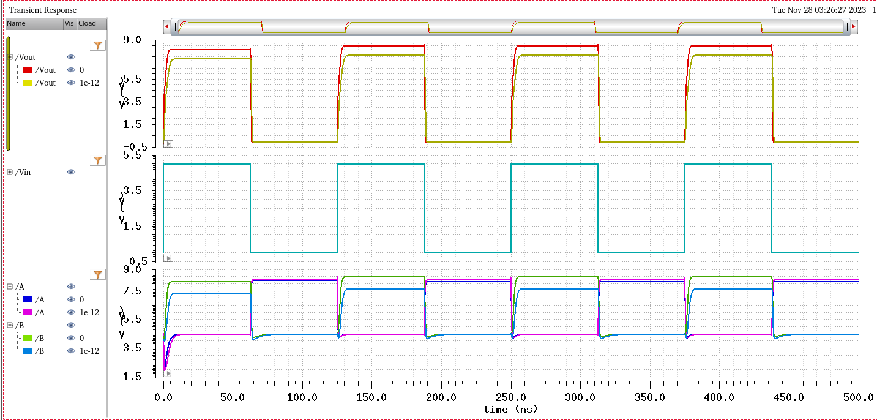
There is some error but for the most part it shows A and B fluctating as close to 2VDD and VDD as I could get it to work.
Layout:
Now
that the schematic has been checked and approved by Dr. Baker for the
first half of project, I can get to work on a matching layout.
One
thing to keep in mind in the layout is how we create the NMOS
capacitors. Normally when we layout MOSFETs of large widths we use
multipliers to create an equivalent sized component without having to
waste much space on the layout. However here it is best to create the
NMOS that are in strong inversion to be both the exact length and width
as we had them in the schematic. This is because the length is also
large here so it wastes less space to have them both L and W to be
large. As a result we end up with the follwing layout.
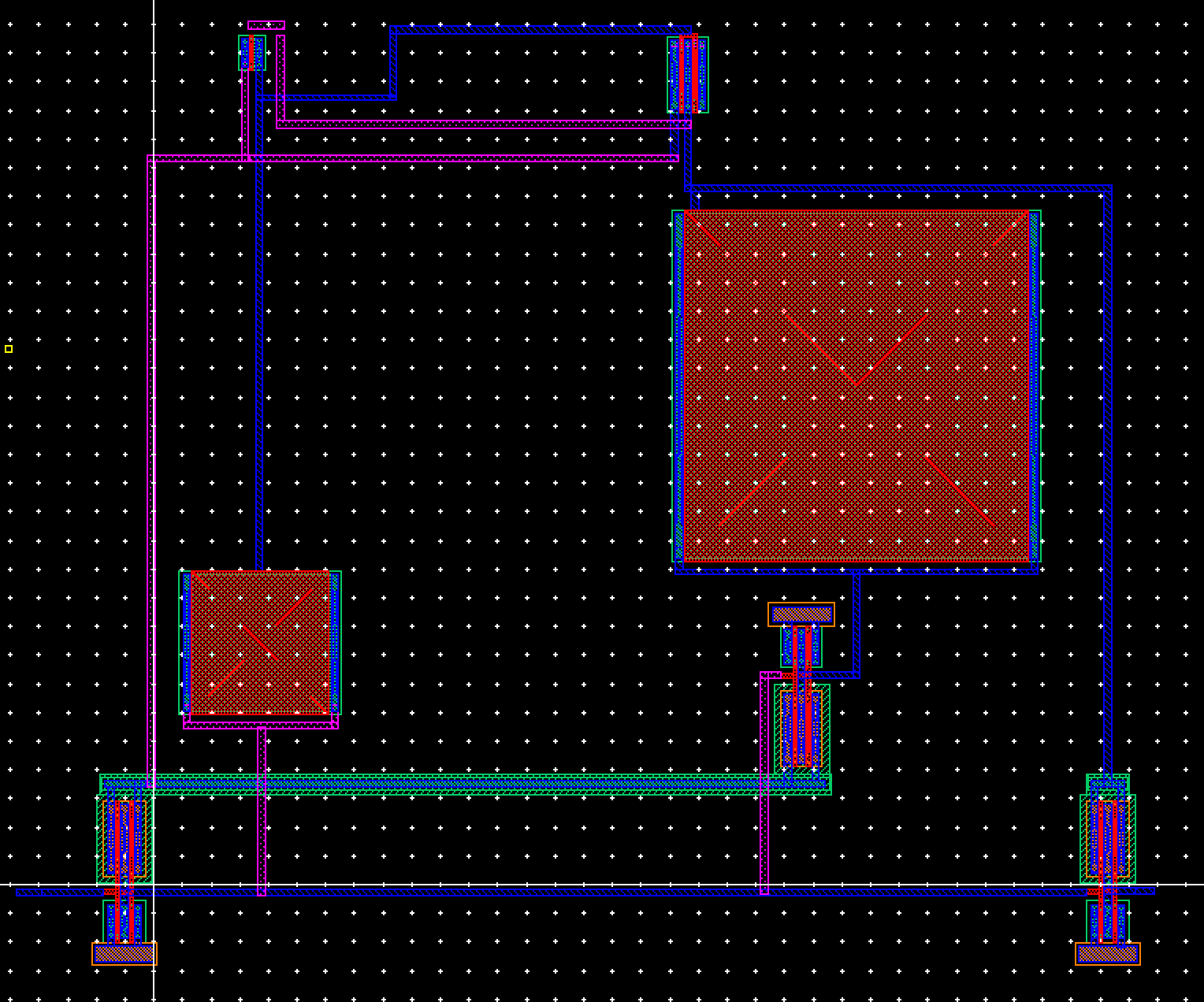
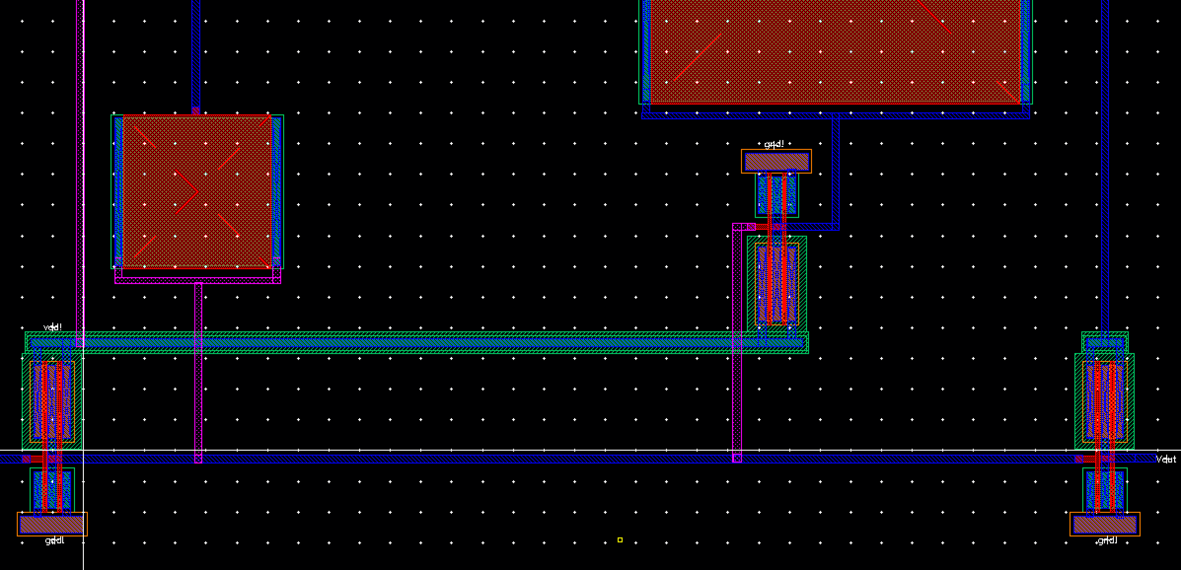
Here are two close up shots for further clarity of the design:
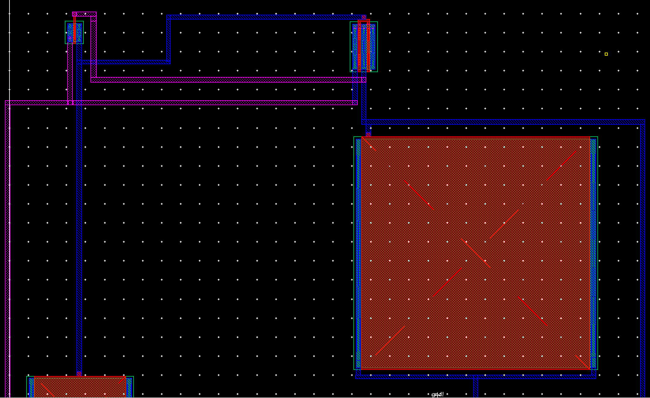 |  |
| The
upper half of the circuit. Here we can see the top 2 NMOS devices in
charge of driving nodes A and B from VDD to 2VDD and the capacitor with
a value of 9pF made by the 60u/60u NMOS in strong inversion. Metal1 and Metal2 are used to prevent merging nets. | The
lower half where we can see the three inverters and the smaller 1.44pF
capacitor made by a 24u/24u NMOS device. Here I tied the first two
inverters together via the ntap so that both of their PMOS's bulk/body
pins were tied to vdd!. The last inverter's PMOS bulk/body is tied to
it's own well so it's ntap goes to node B. |
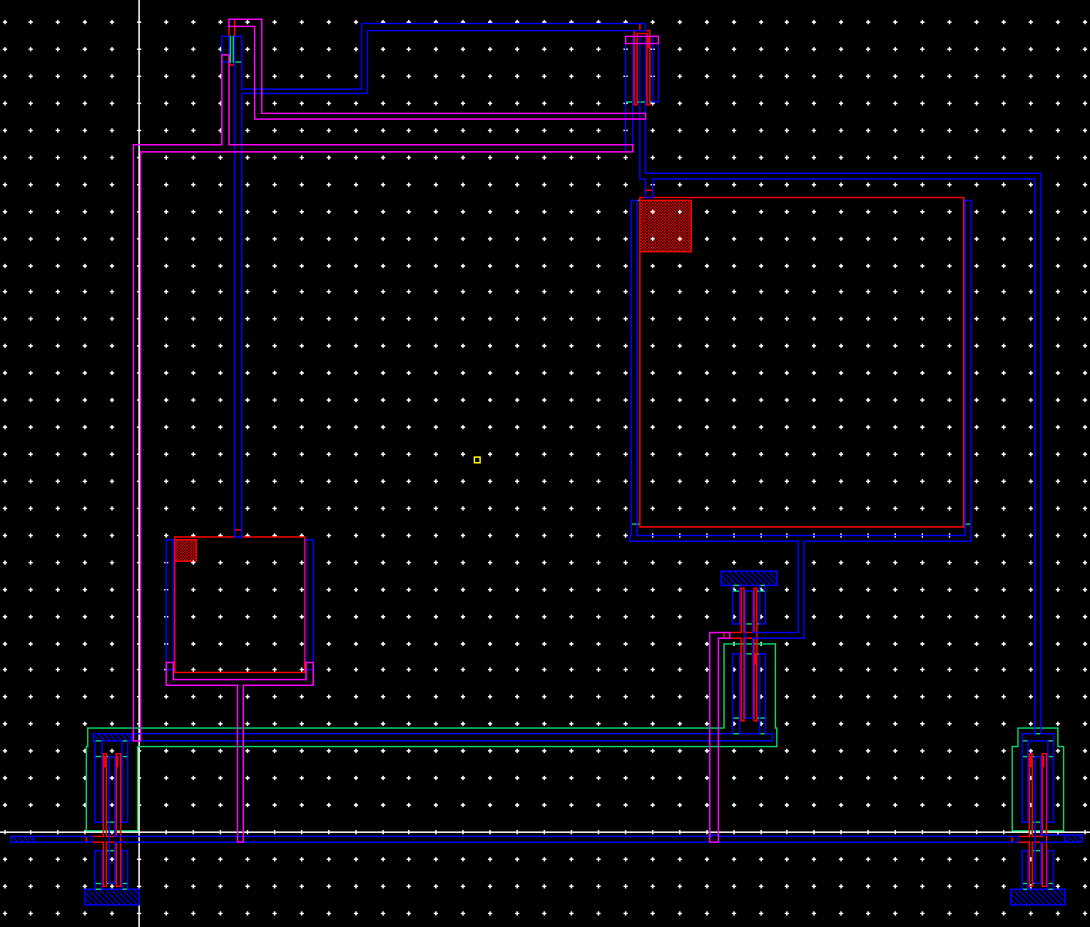
The resulting extraction is shown here:
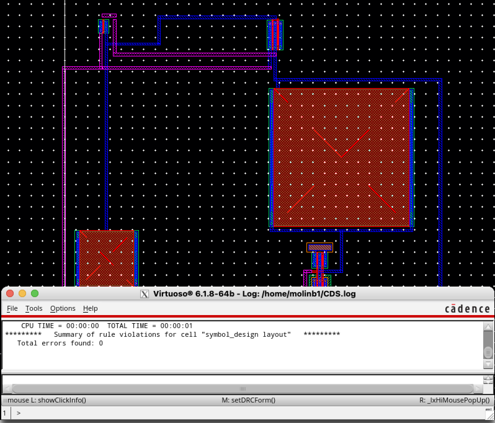
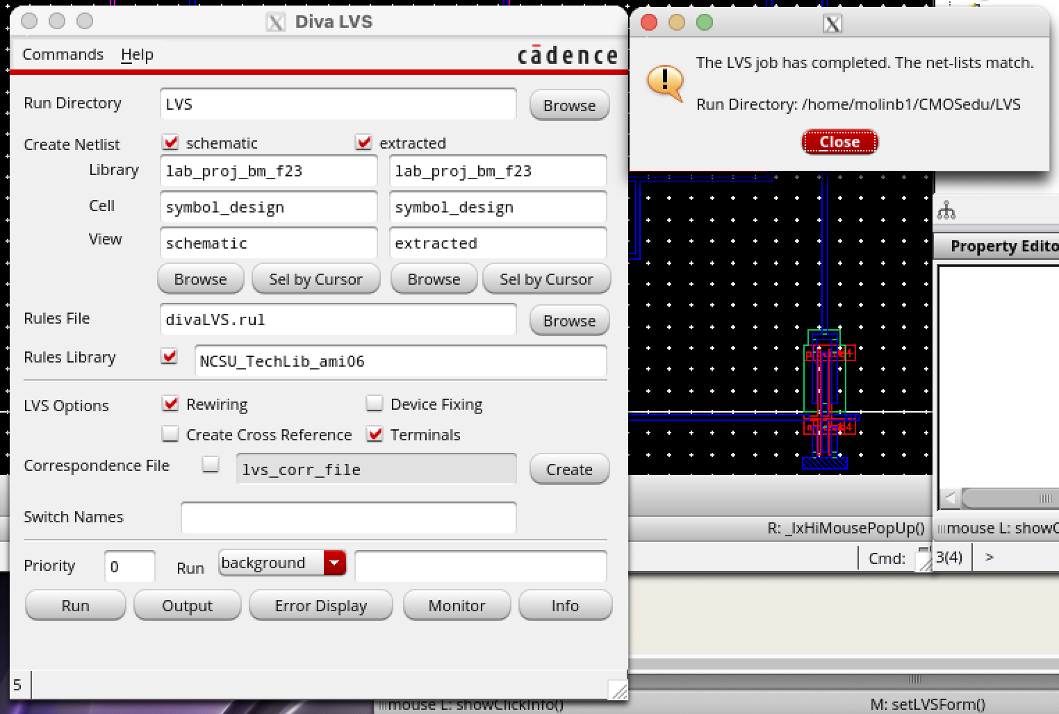
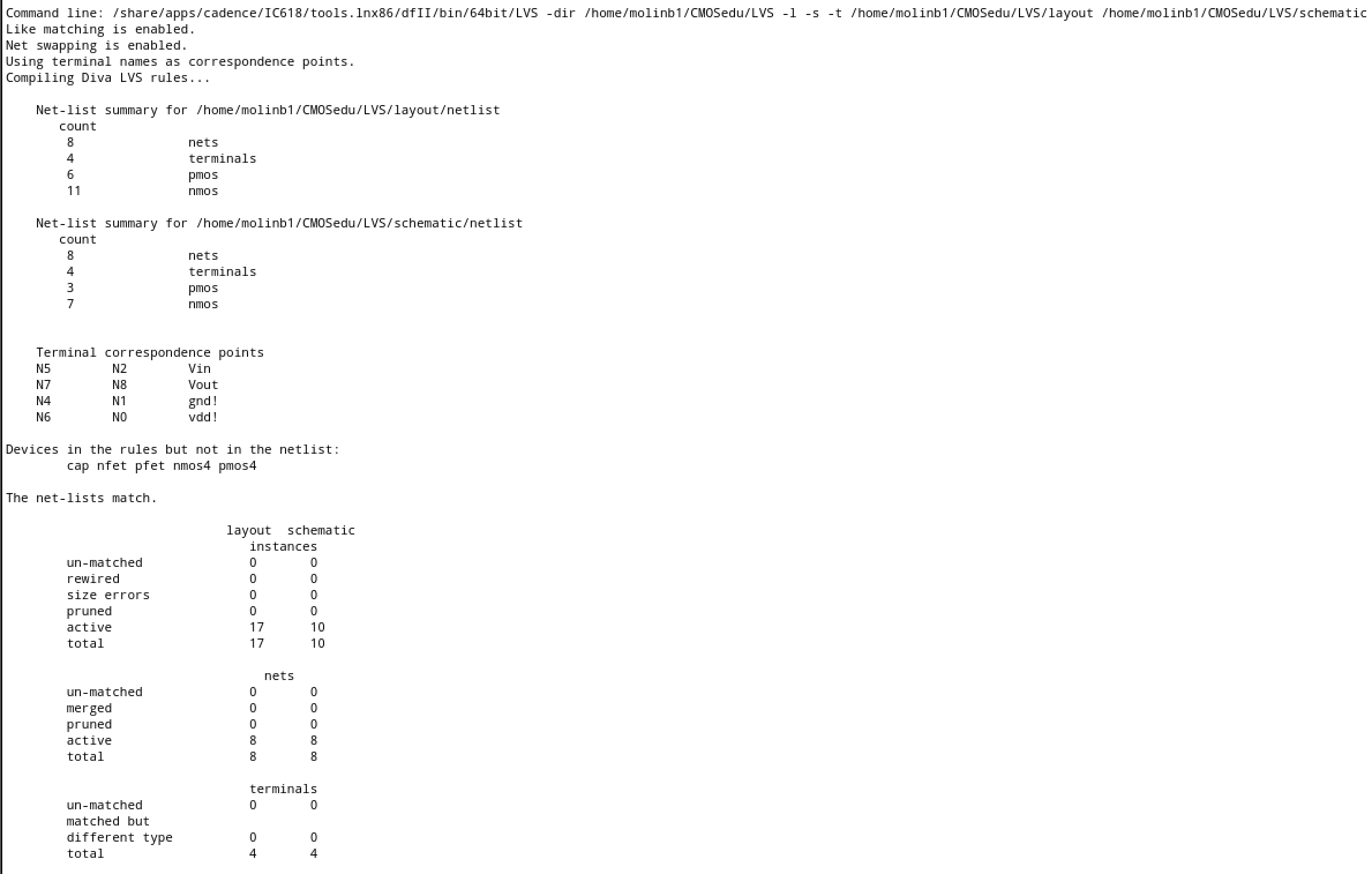
The DRC and LVS are shown here:
| DRC | LVS |
 |  |
All work done in Cadence has been saved on this zip file: BM_f23_labproj.zip
Return to EE 421L Labs