Lab 7 - ECE 421L
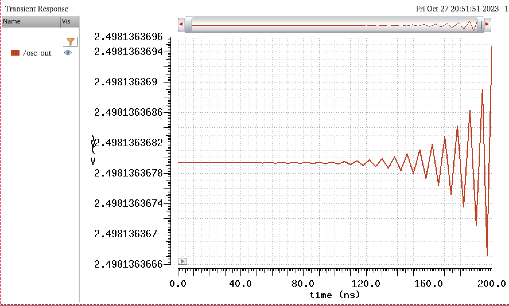
| Ring Oscillator Design: | Simulation without initial condition: |
| |
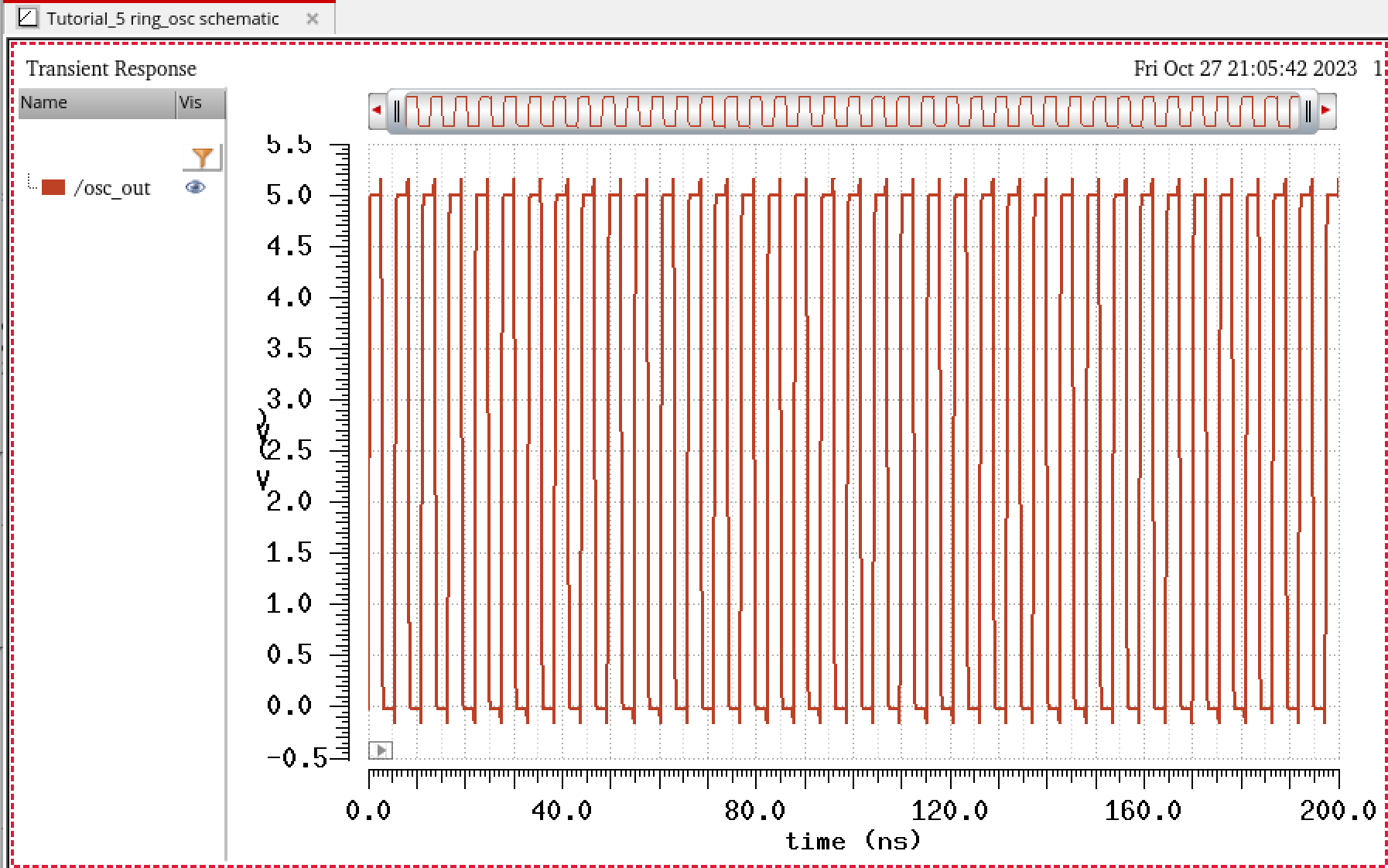
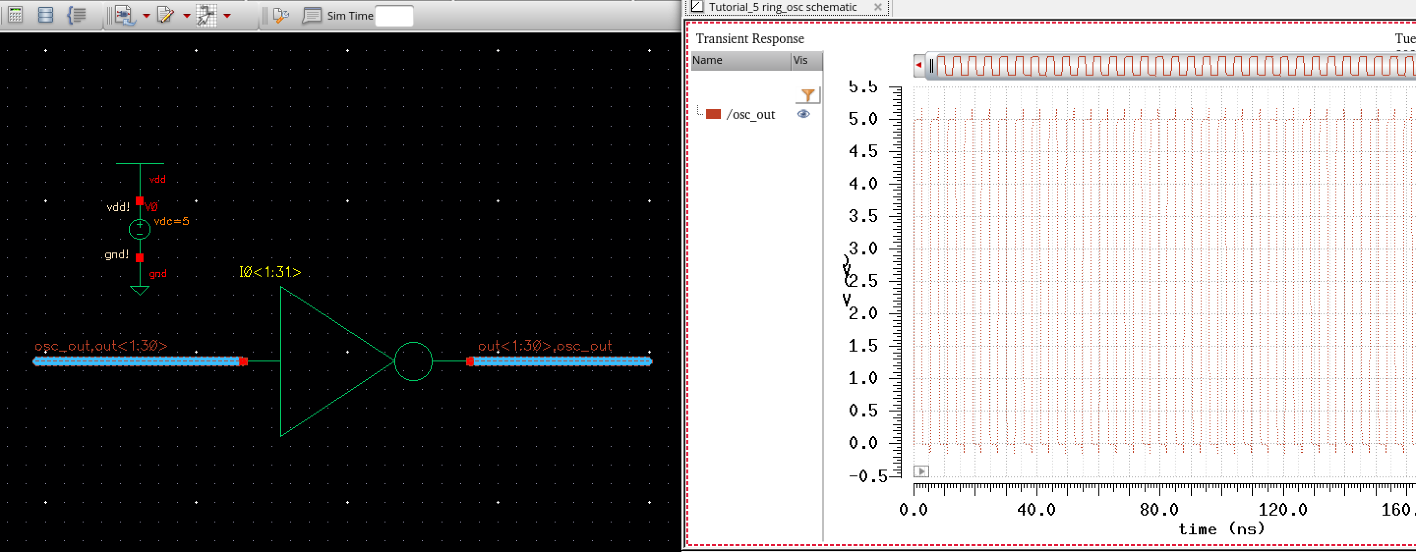
| Simulation with initial condition set to "0": | Concise schematic and simulation: |
| |
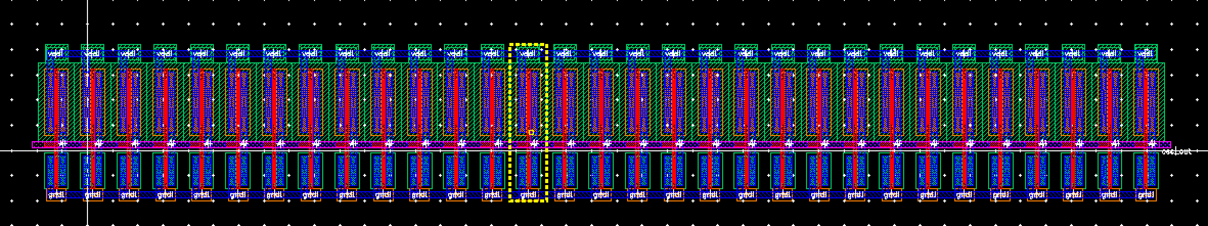
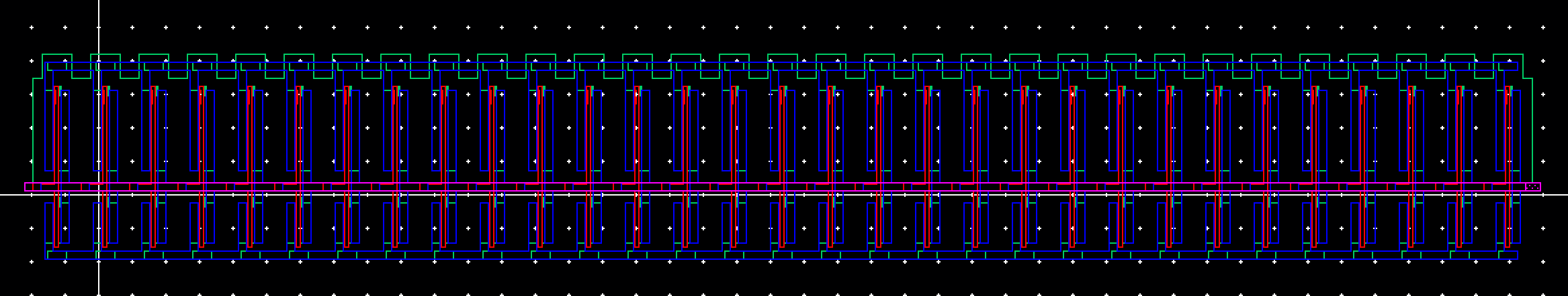
| Ring Oscillator Layout: | Ring Oscillator Extracted: |
| |
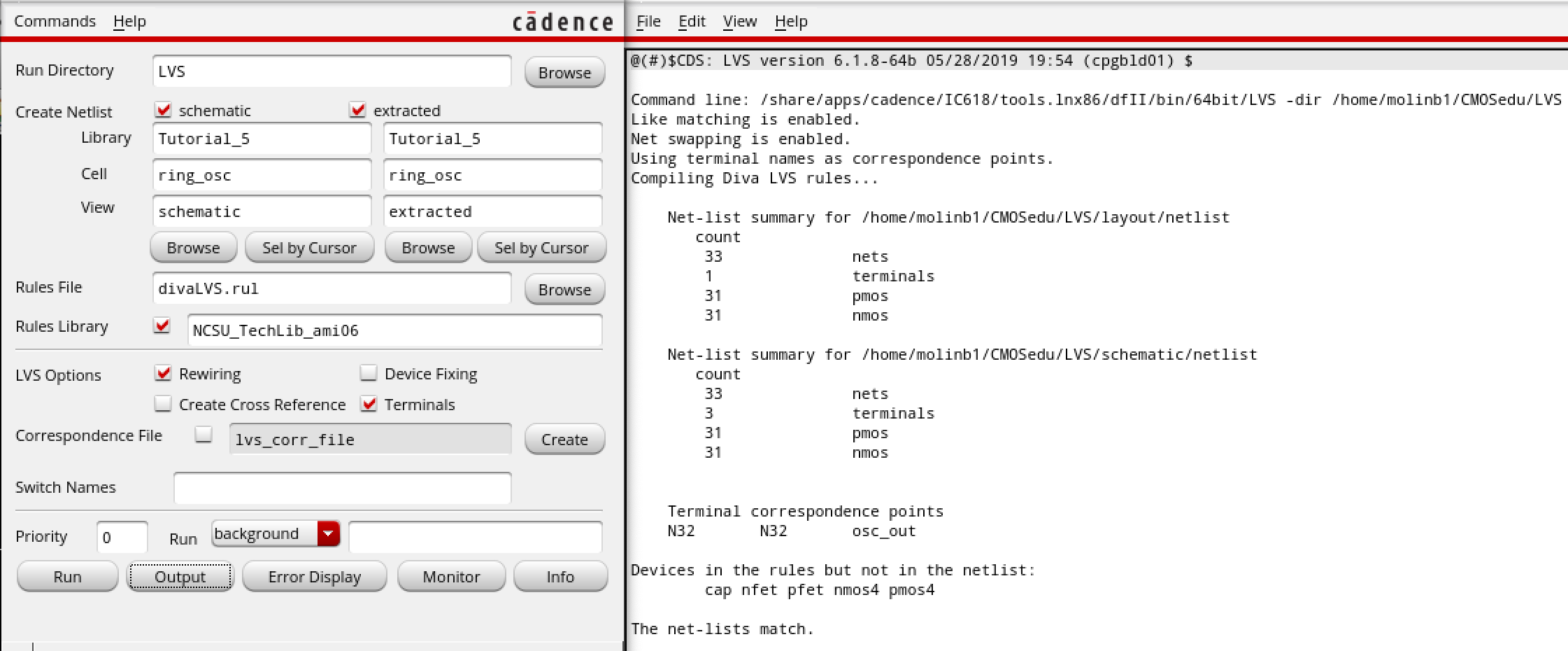
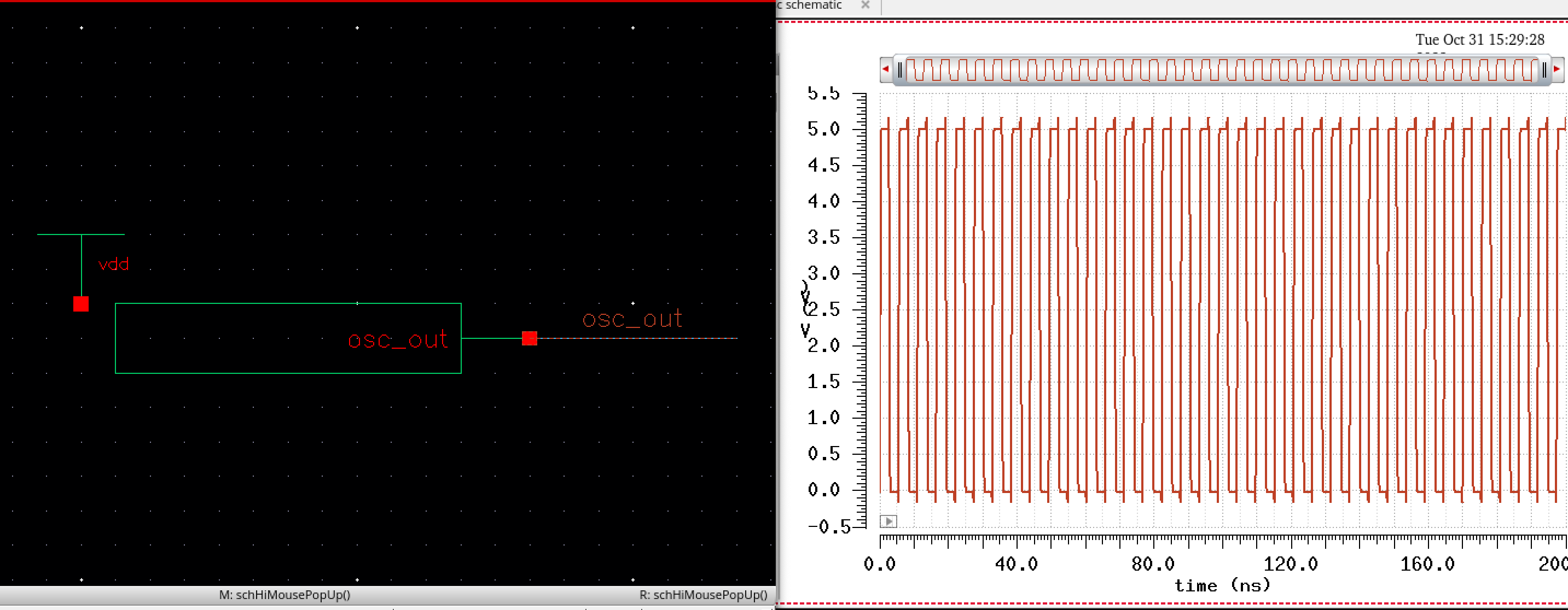
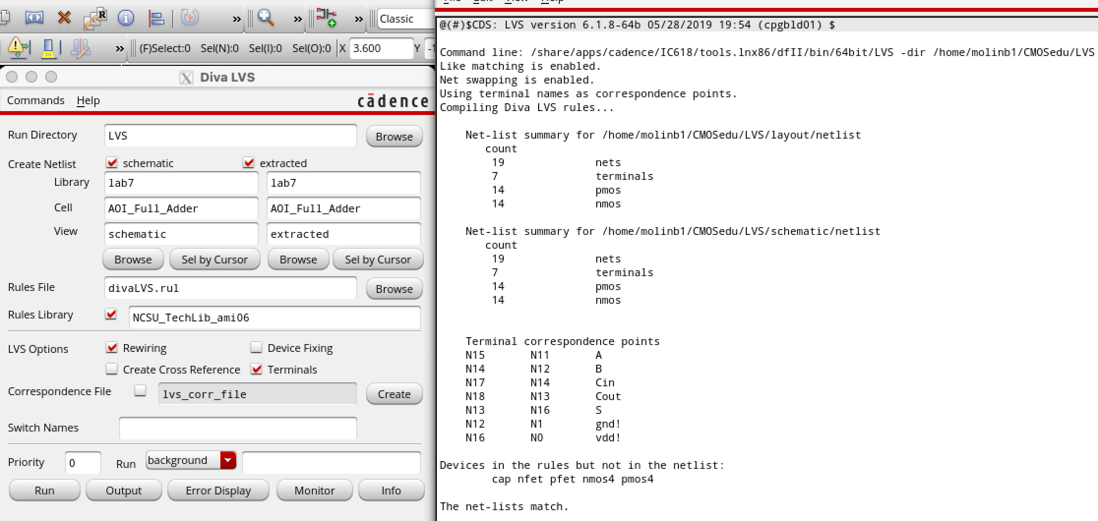
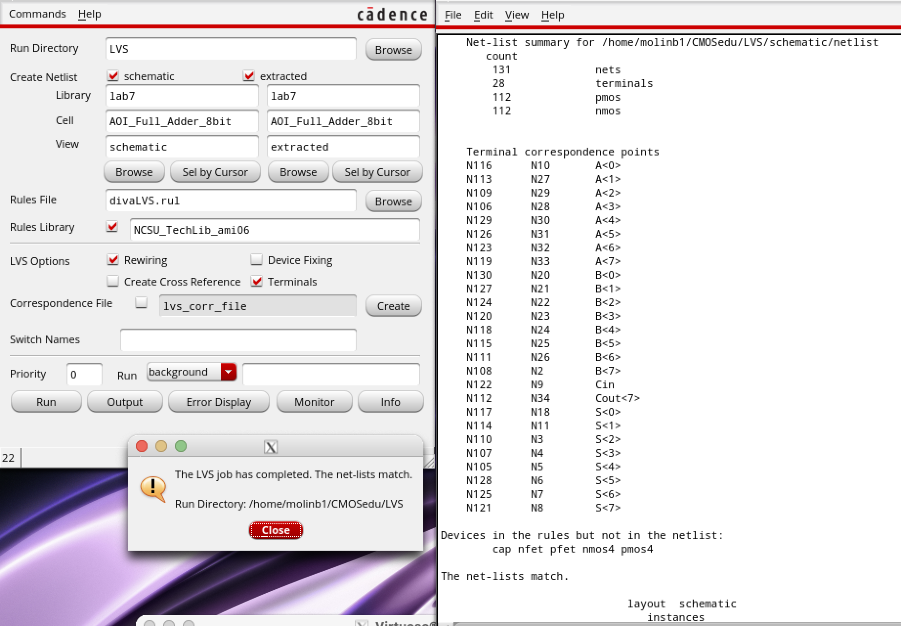
| LVS: | Ring Oscillator Symbol Simulation: |
| |
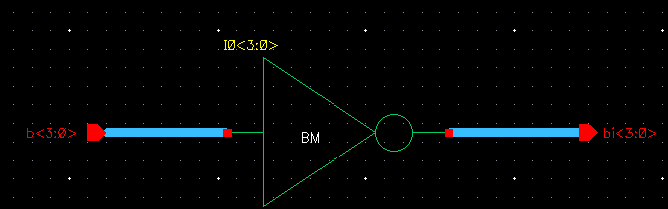
| Schematic | Symbol |
 | 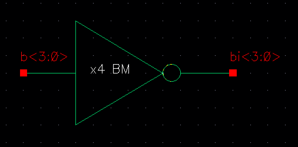 |
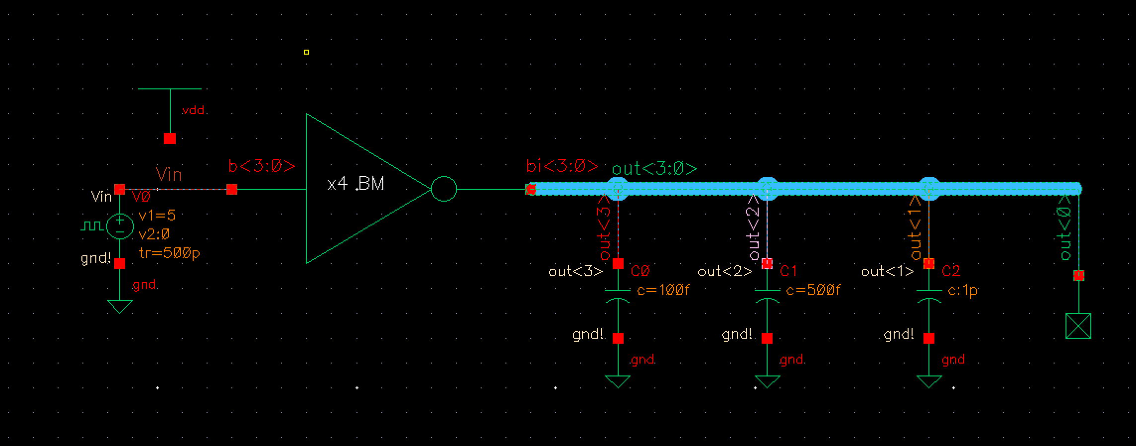
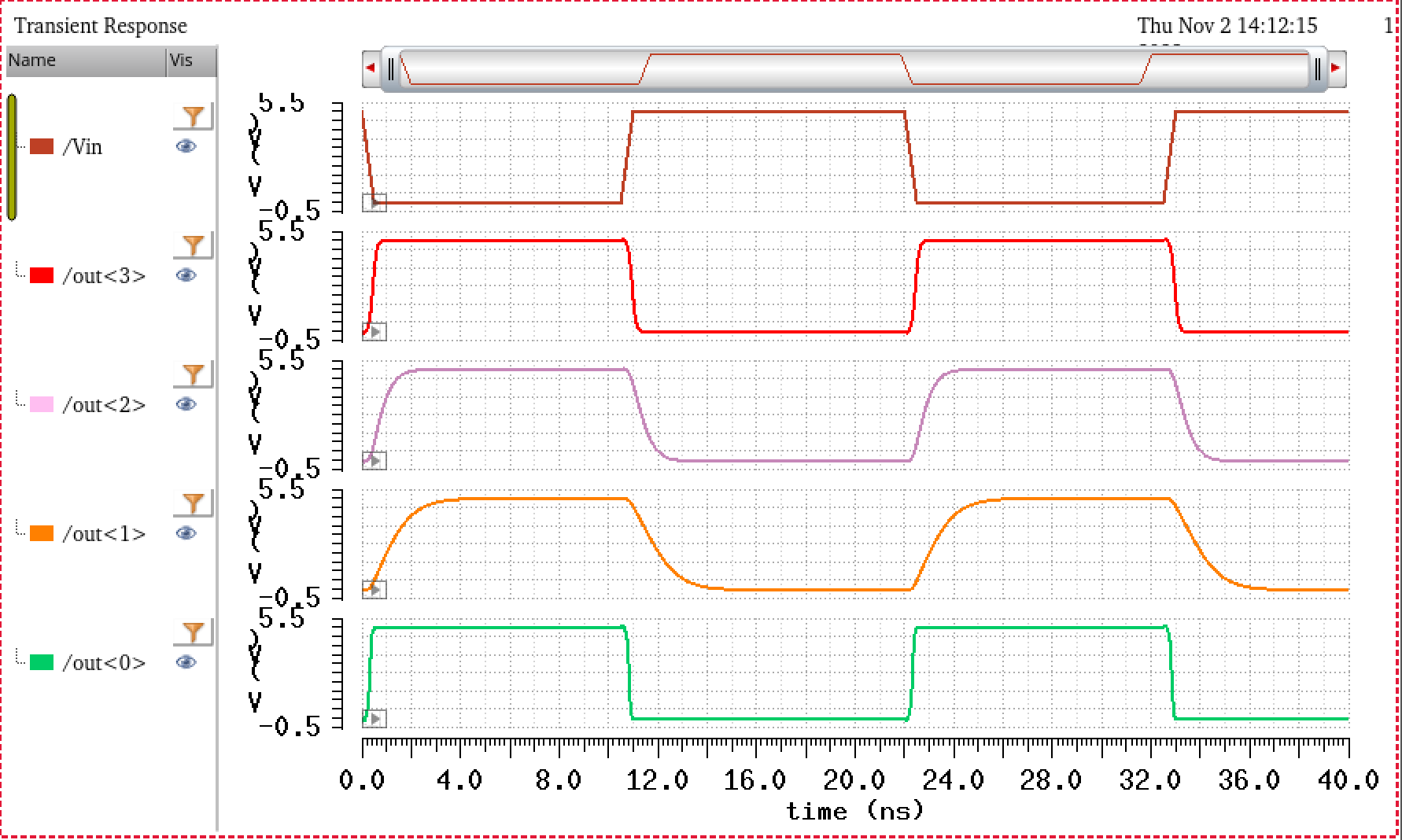
| 4-bit Schematic | 4-bit Simulation |
 |  |
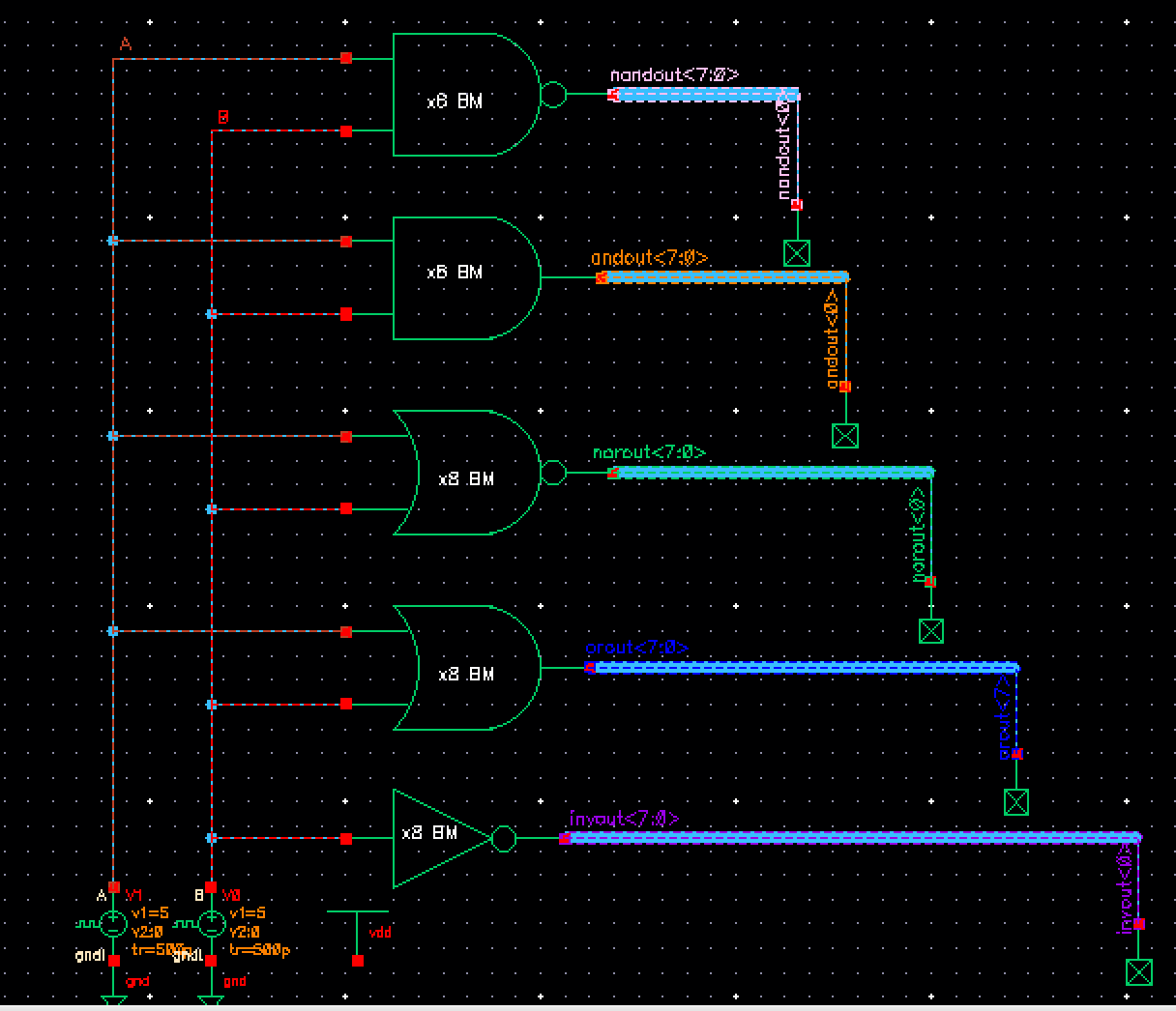
| 8-bit Schematic | 8-bit Symbol | CMOS Schematic | |
| NAND | 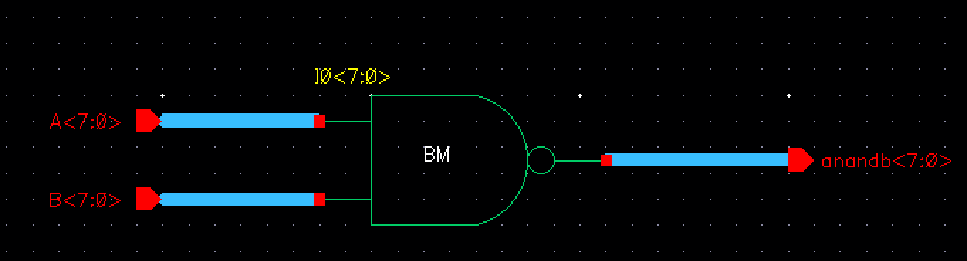 | 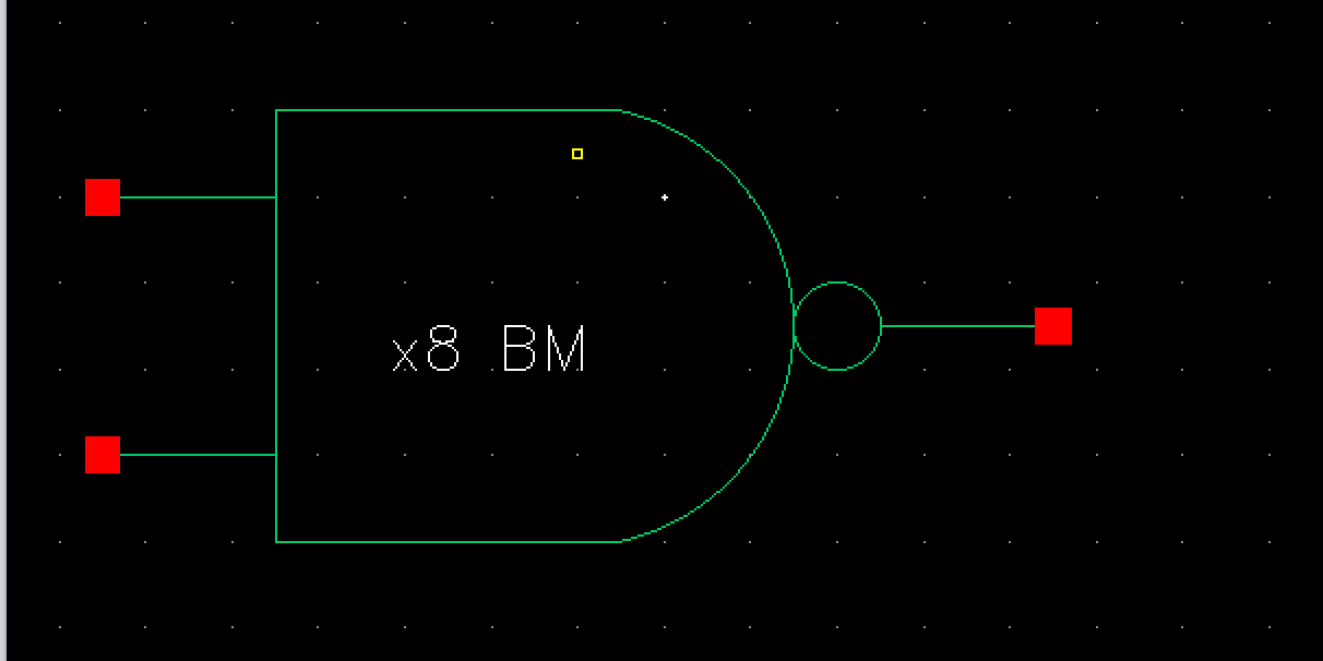 | 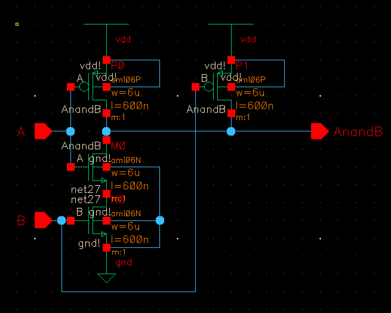 |
| AND | 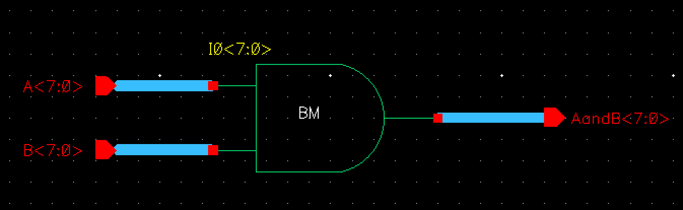 | 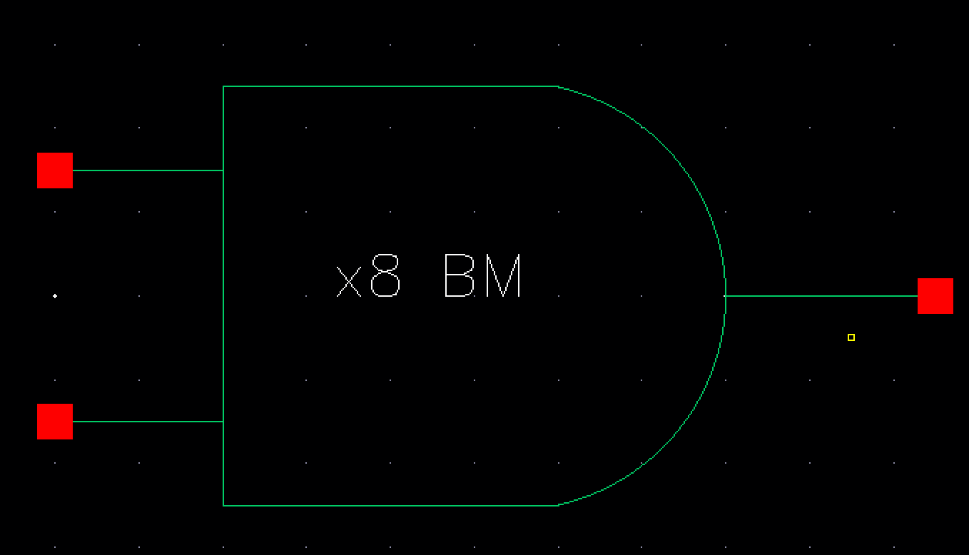 | 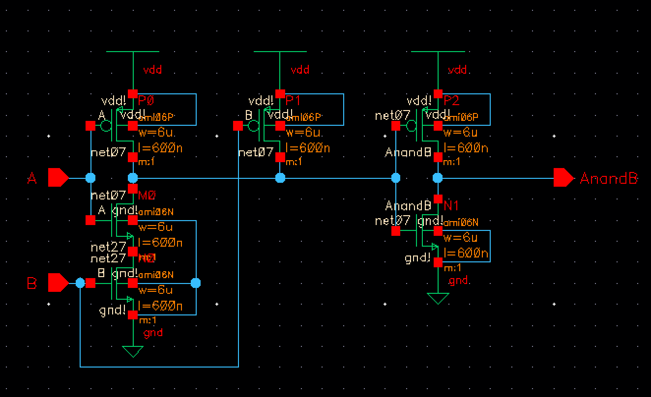 |
| NOR | 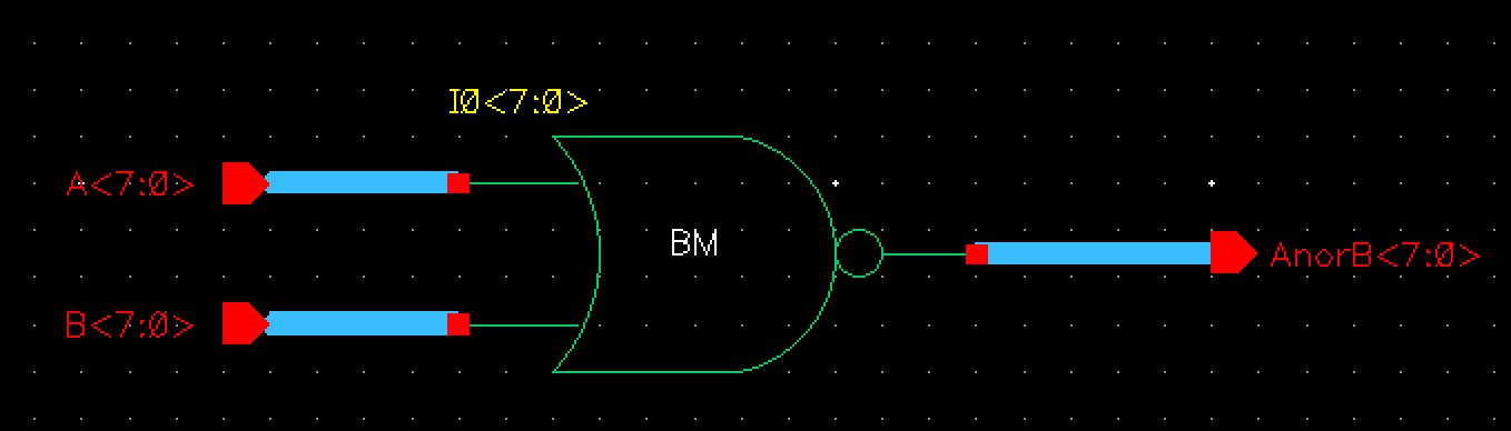 | 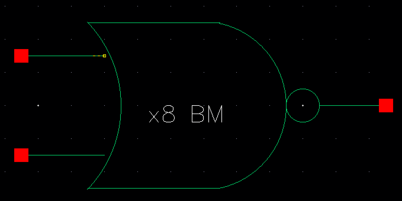 | 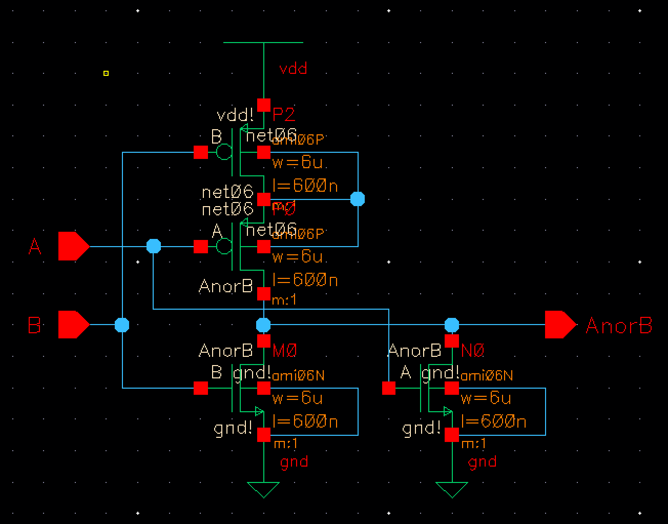 |
| OR | 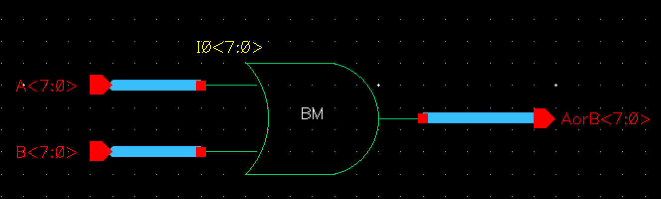 | 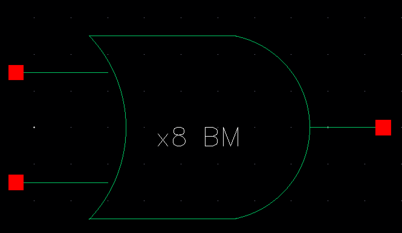 | 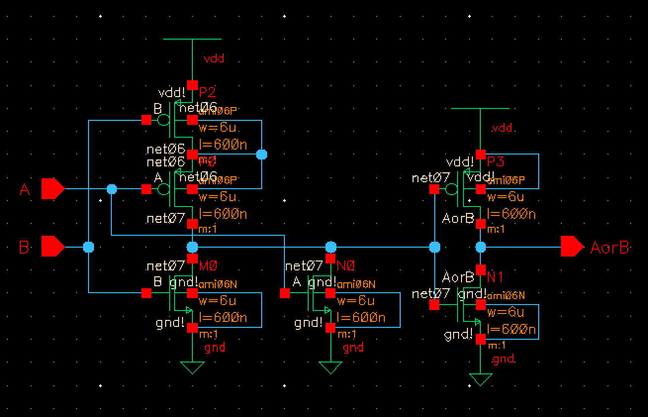 |
| NOT | 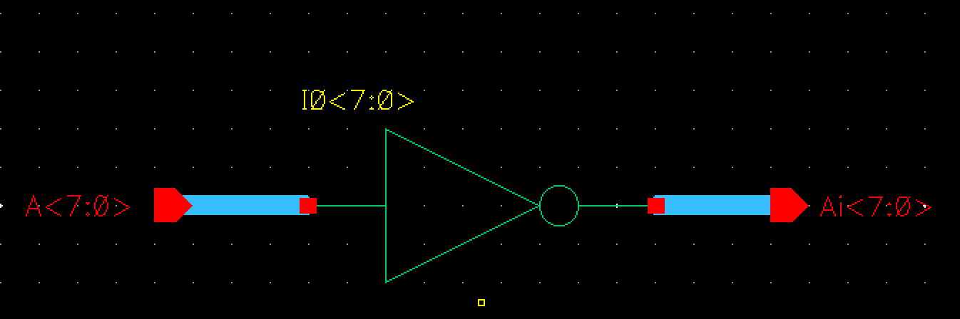 | 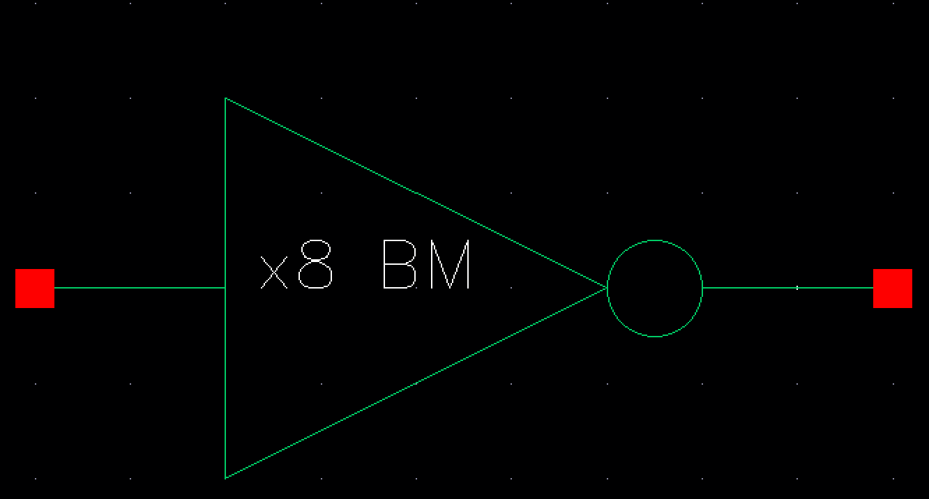 | 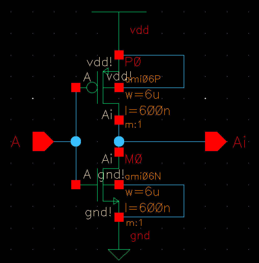 |
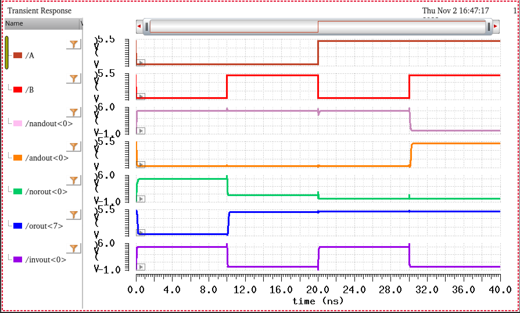
| Schematic: | Simulation: |
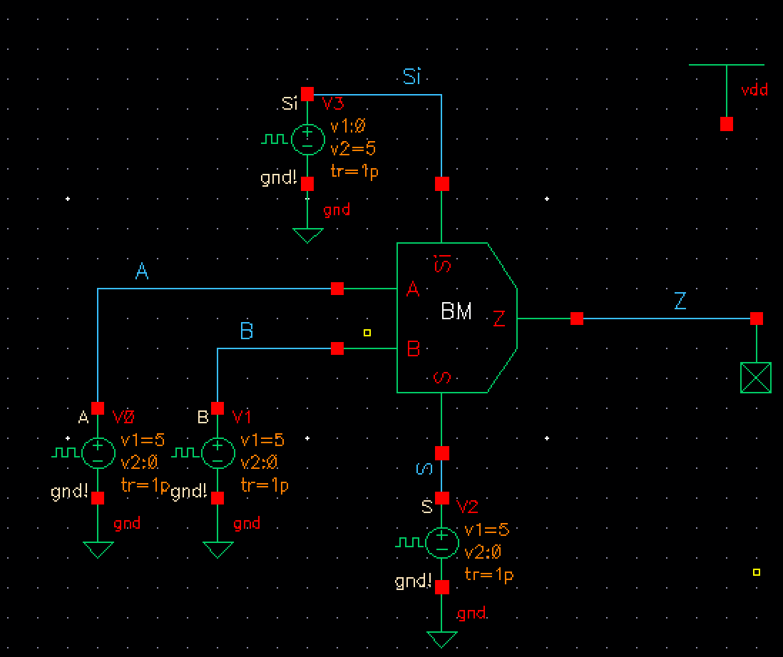 | 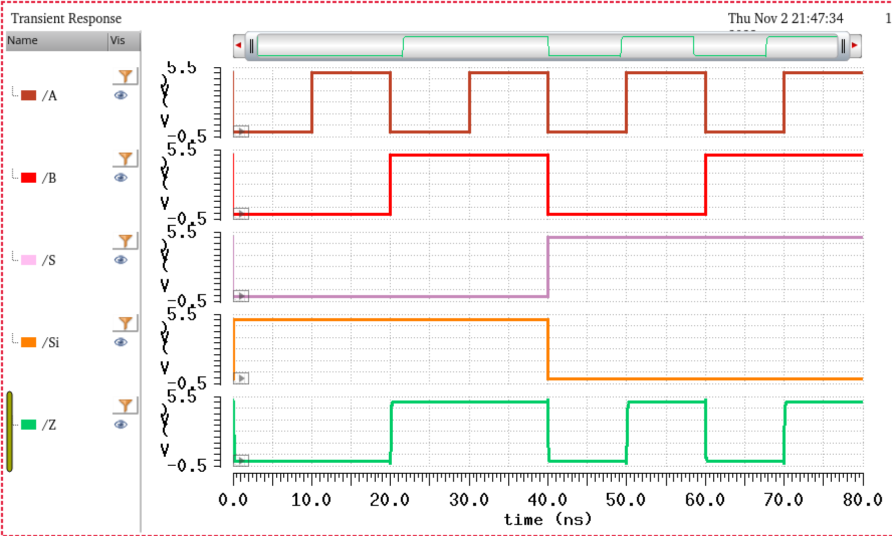 |
| MUX/DEMUX Schematic | Symbol |
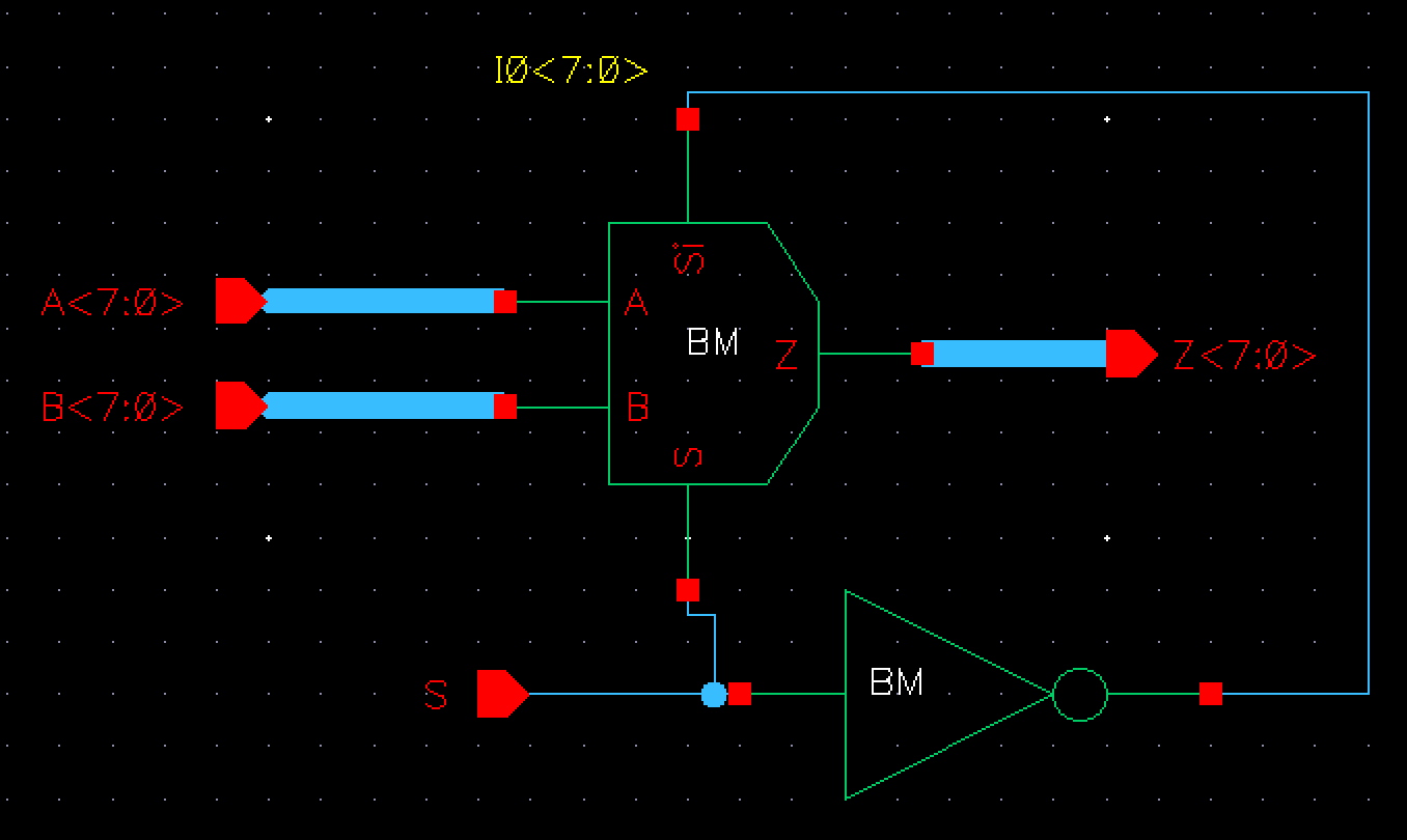 |  |
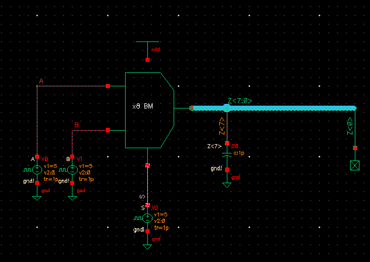
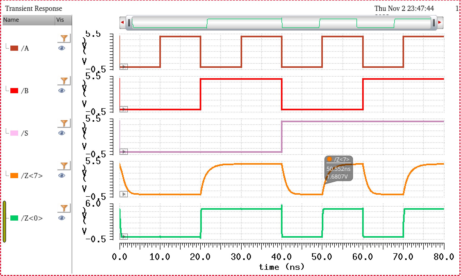
| 8-Bit MUX | 8-Bit MUX Simulation |
 |  |
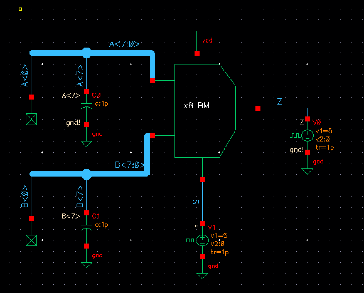
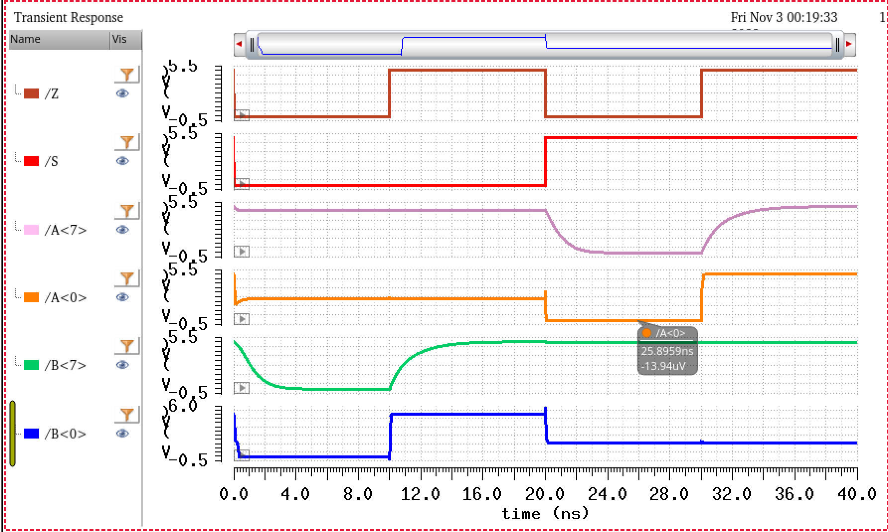
| 8-Bit DEMUX | 8-Bit DEMUX Simulation |
 |  |
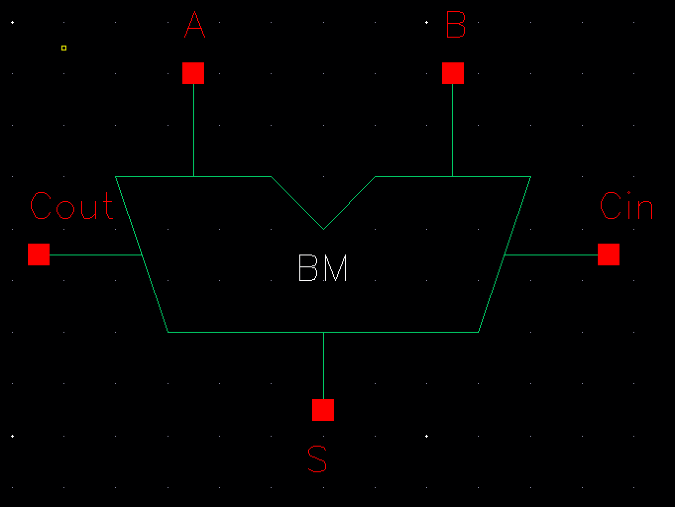
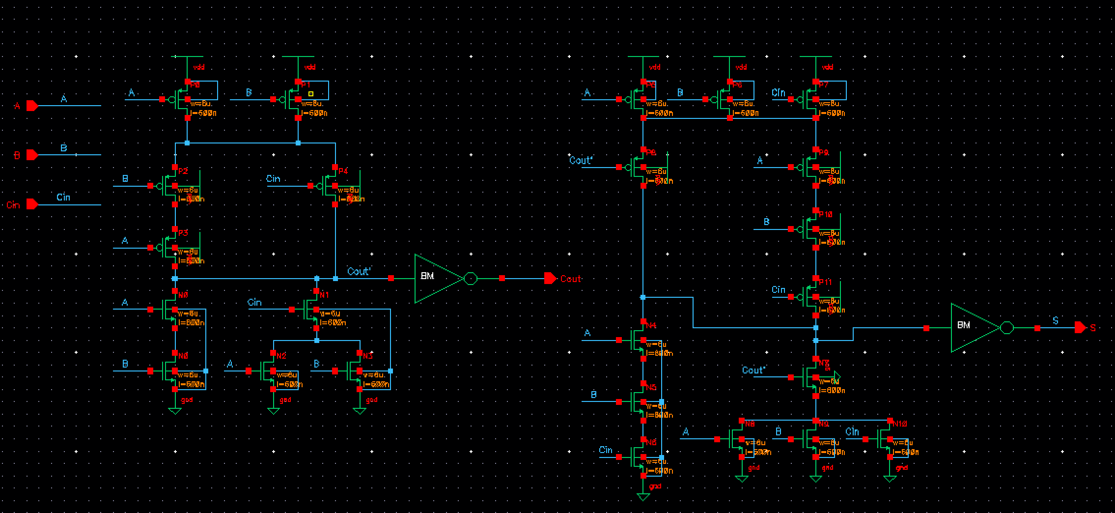
| Full Adder CMOS Schematic |
 |
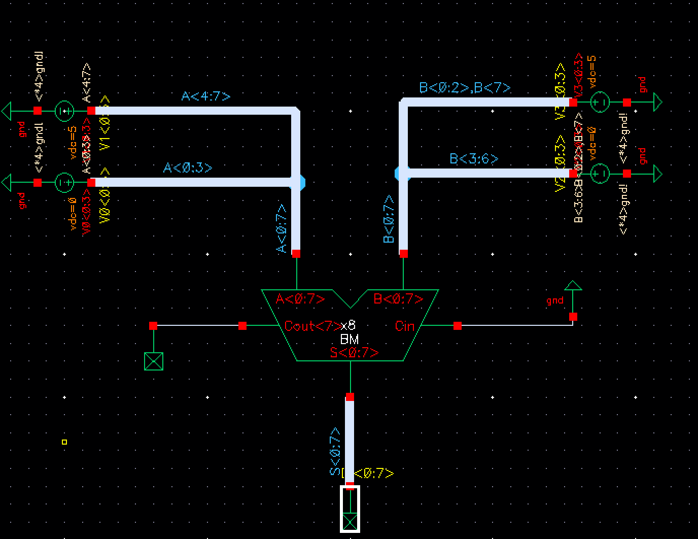
| 8-Bit Adder Schematic |
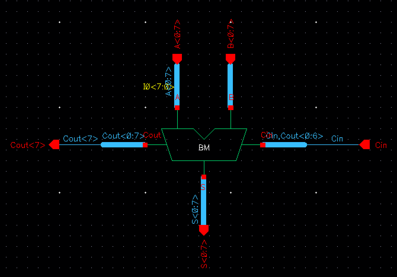 |
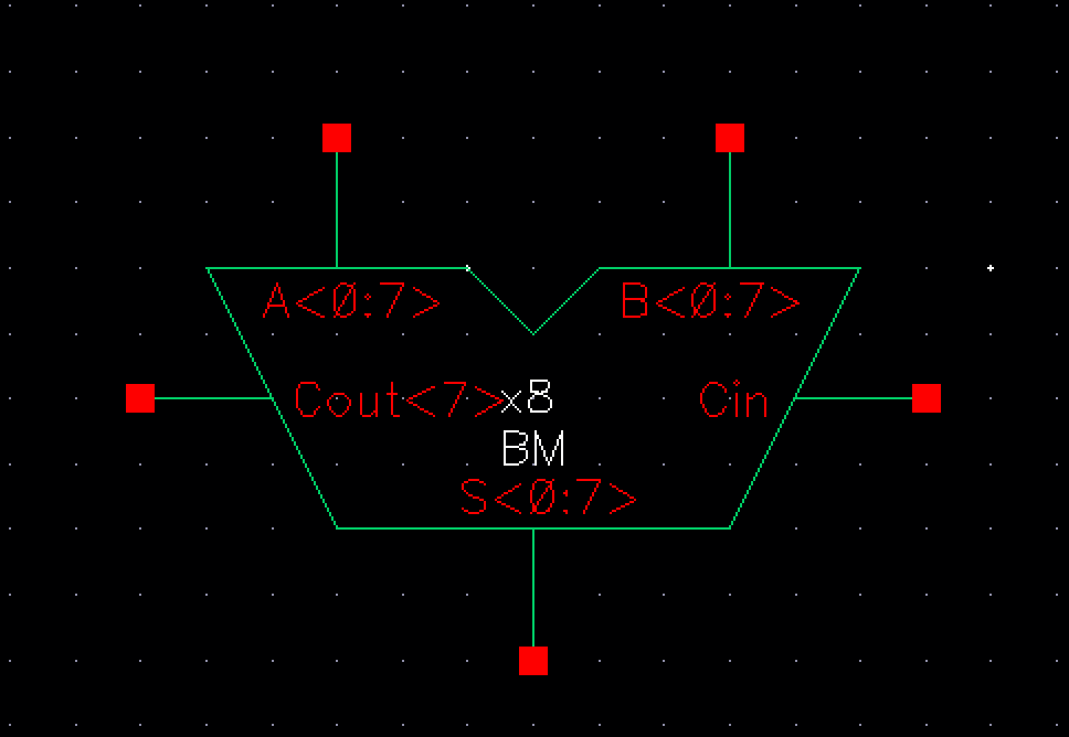
| 8-Bit Symbol |
 |
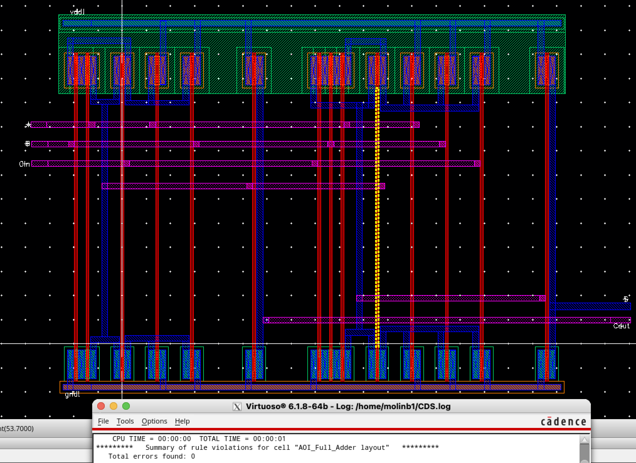
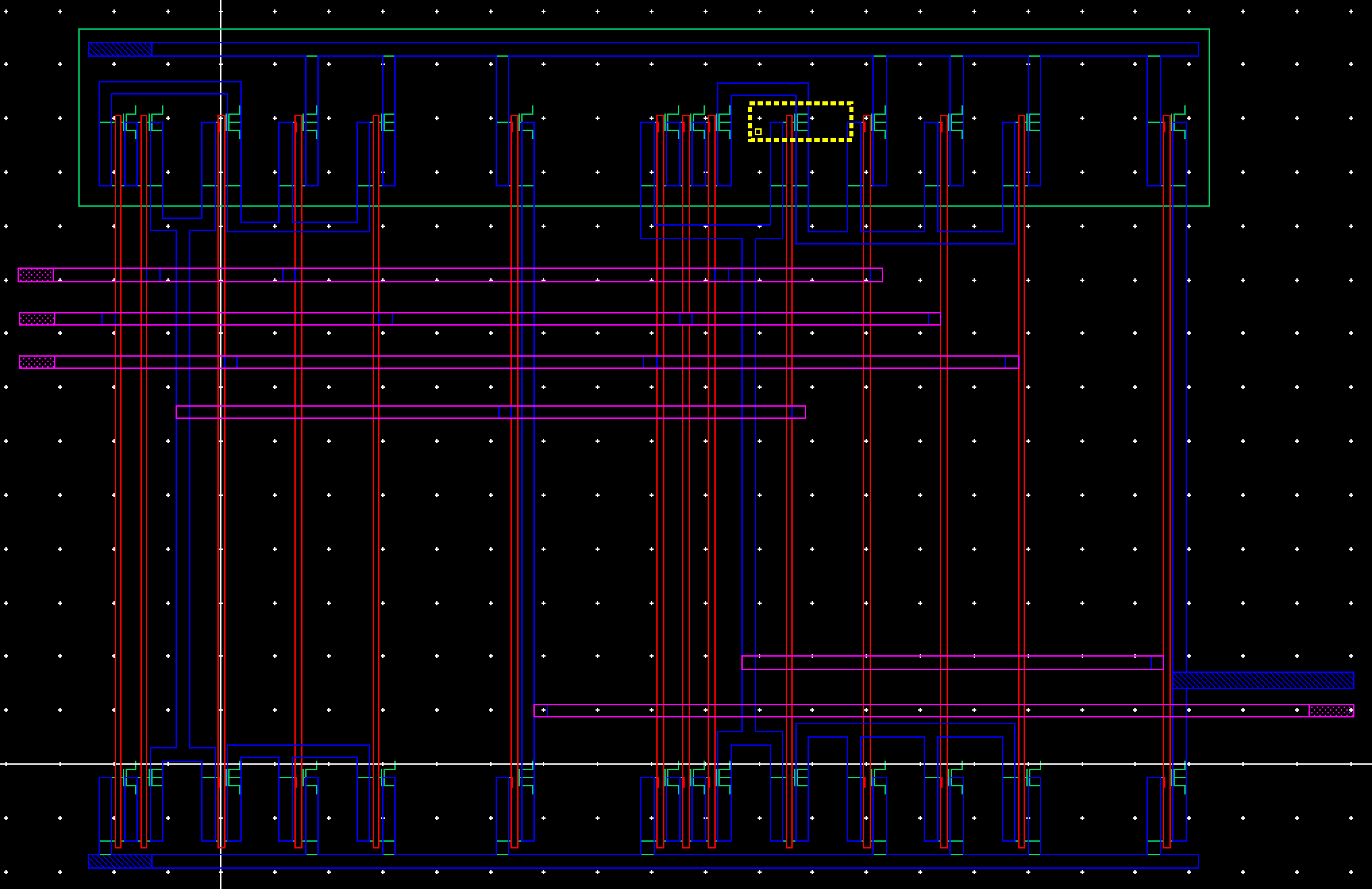
| 1-Bit Full Adder/DRC | Extracted 1-Bit Full Adder |
 |  |
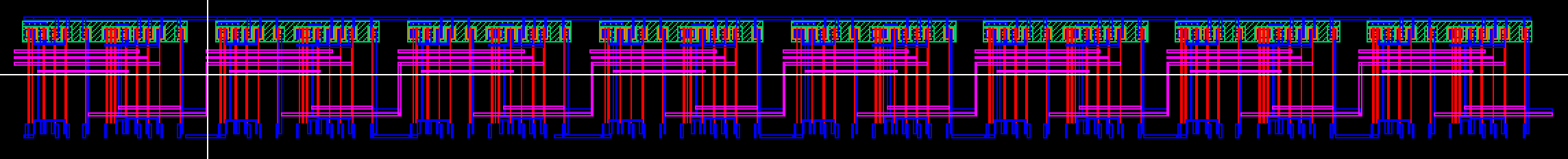
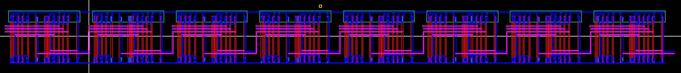
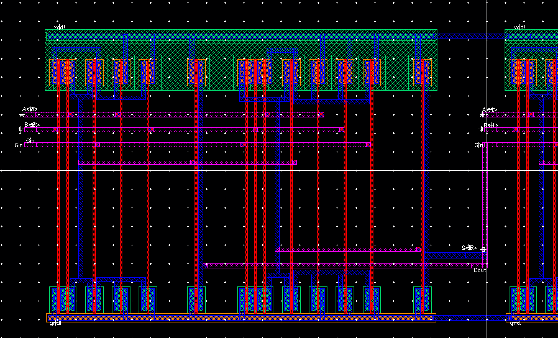
| 8-Bit Full Adder | Extracted 8-Bit Adder |
 |  |
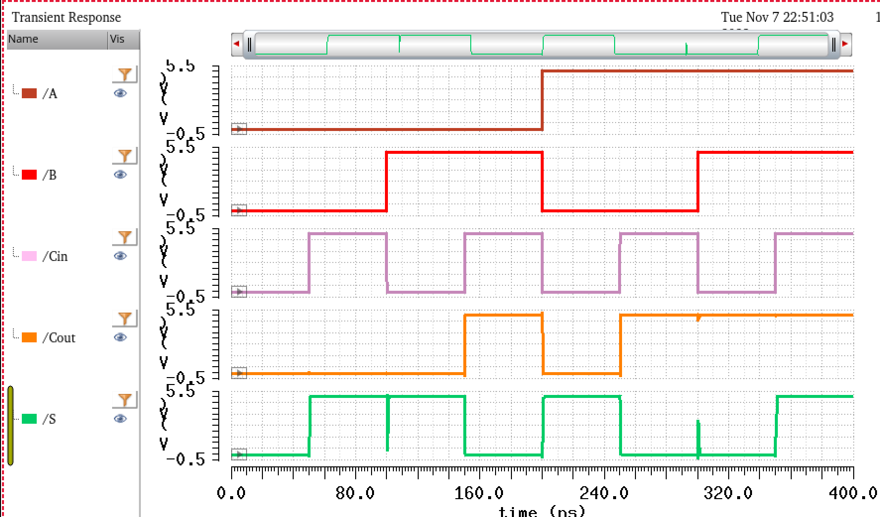
| Schematic | Simulation |
 |  |