Lab 5 - ECE 421L
Authored
by Benjamin Molina, molinb1@unlv.nevada.edu
10/6/2023
Prelab:
The
first step of the prelab involved simply ensuring that previous labs
and wrok have been backed up and saved properly. The second part was to
go through Tutorial 3 posted on CMOSedu which involved the basic
creation of an inverter using a PMOS and an NMOS.
| Schematic of inverter using NMOS and PMOS | 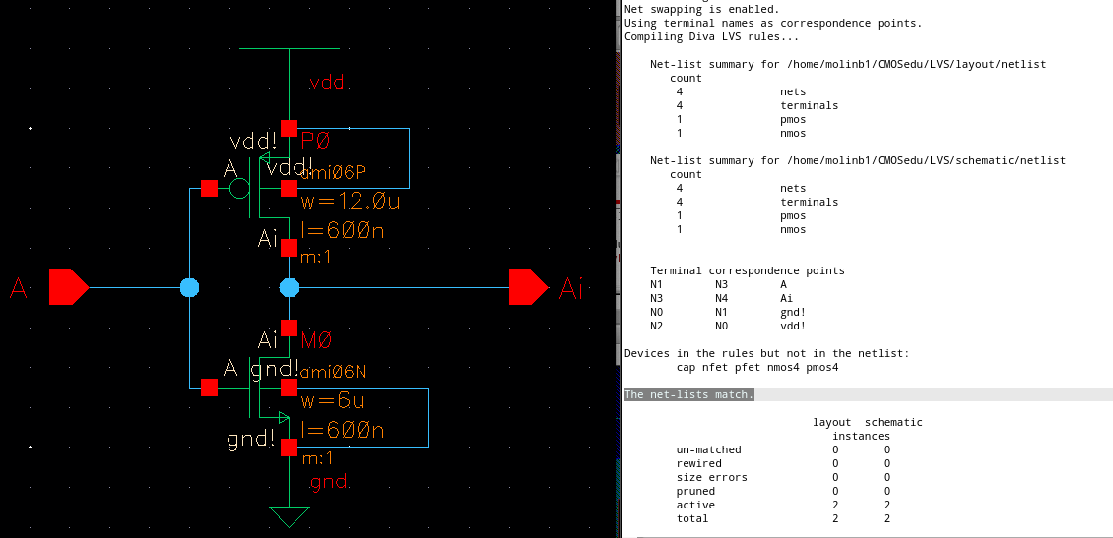 |
| Schematic of inverter in use. Using a hand made symbol. | 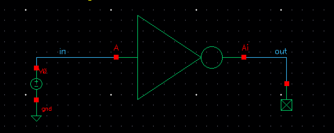 |
| Outout of the inverter compared to input. | 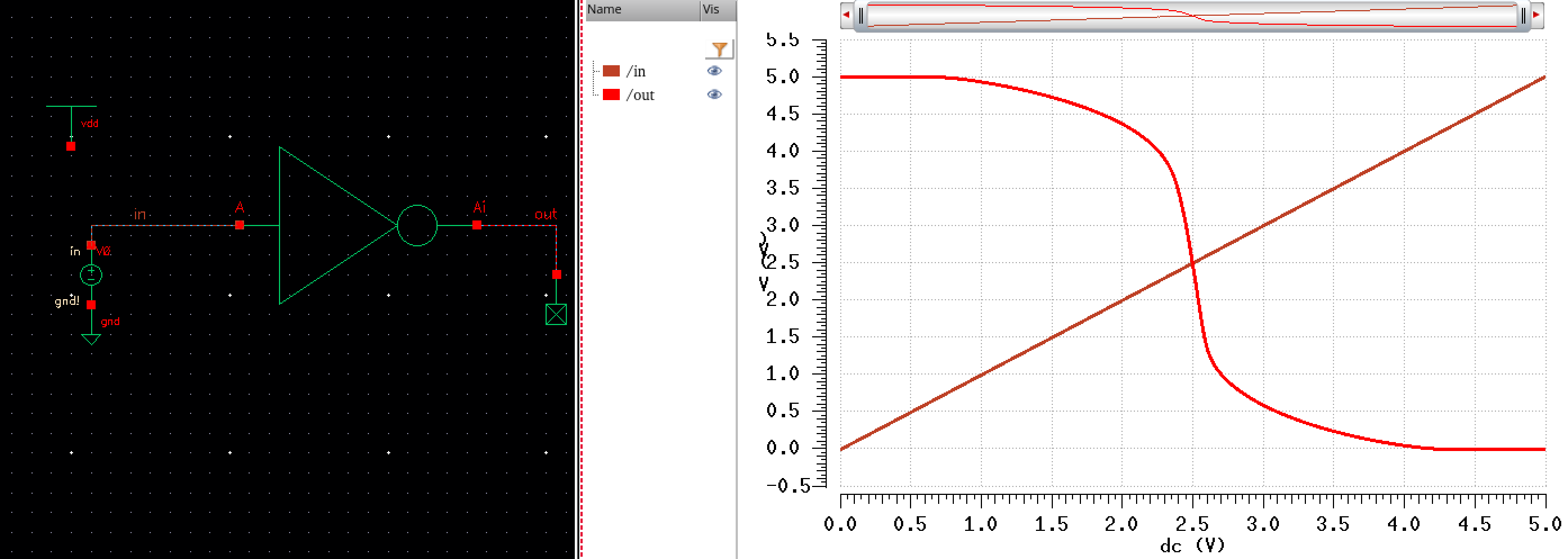 |
| Extracted view output vs input simulation. | 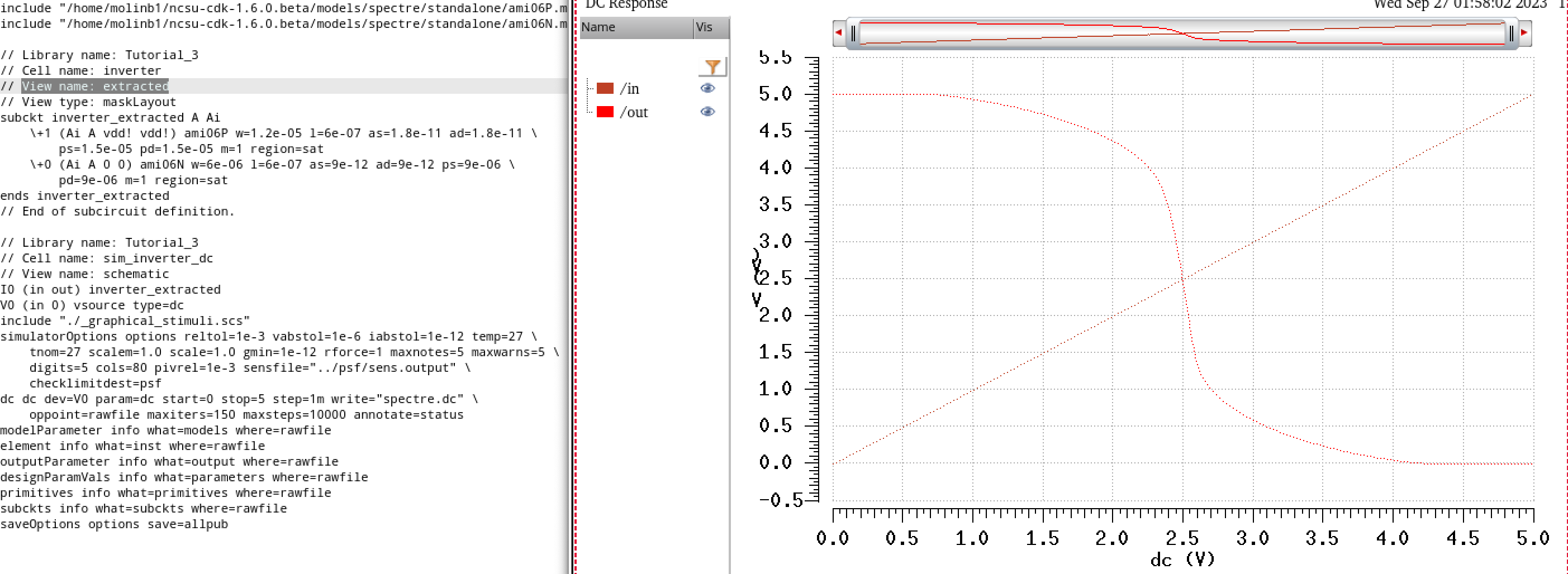 |
Lab Procedure:
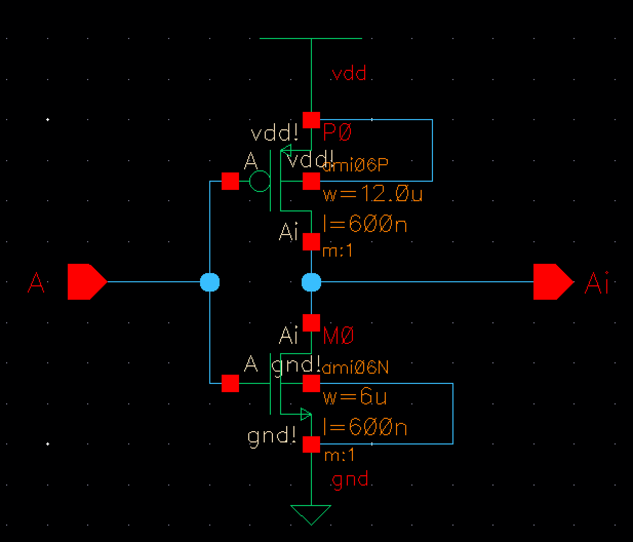
Creation of 12u/6u Inverter:
The
first step we must perform is the creation of a 12u/6u inverter. This
was done already in Tutorial 3 so for convienvce we will simply reuse
what we created previously for this part.
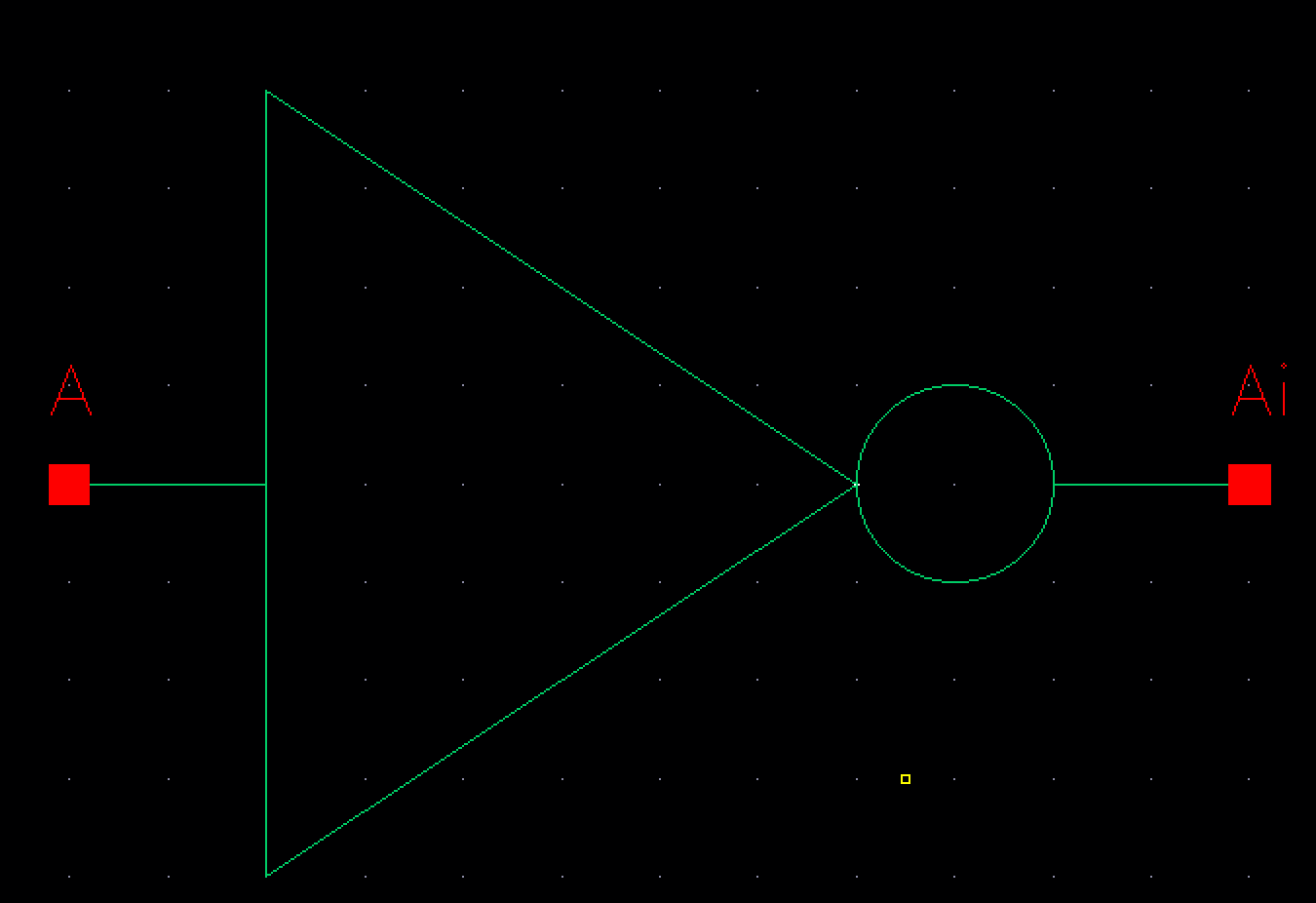
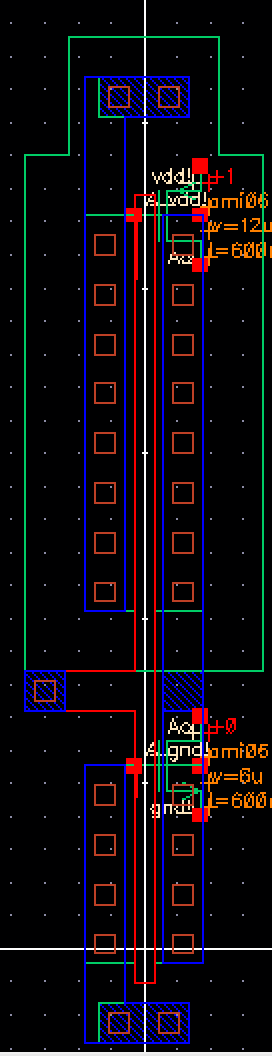
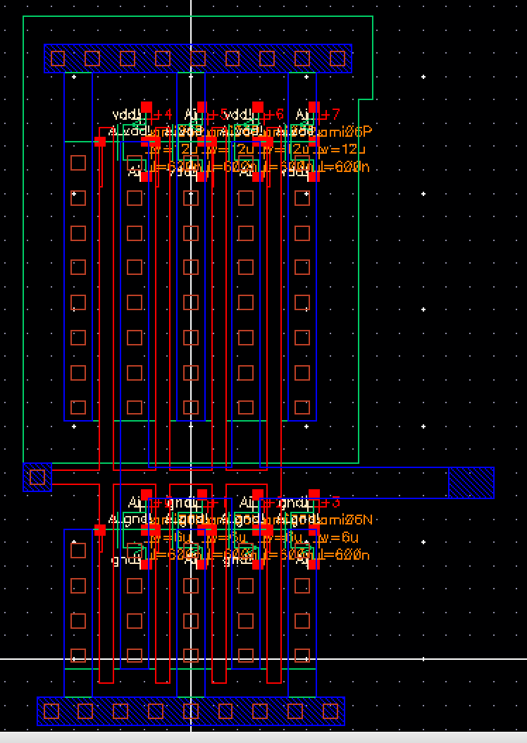
We must create an inverter schematic, symbol, layout and extracted view.
| 12u/6u Inverter Schematic | 12u/6u Inverter Symbol | 12u/6u Inverter Layout | 12u/6u Inverter Extracted View |
 |  | 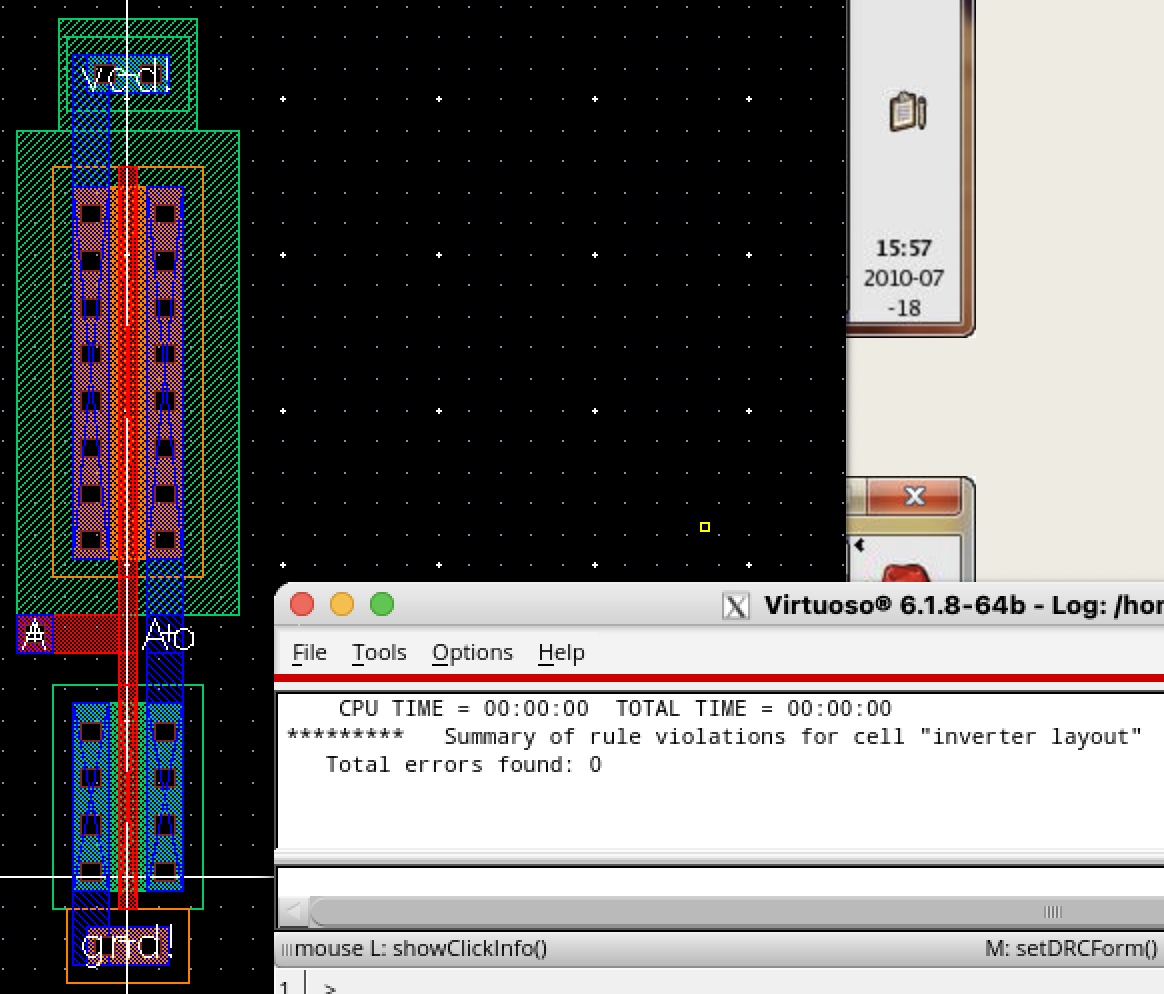 |  |
Now we need to prove that the extracted view and the schematic match with an LVS check.
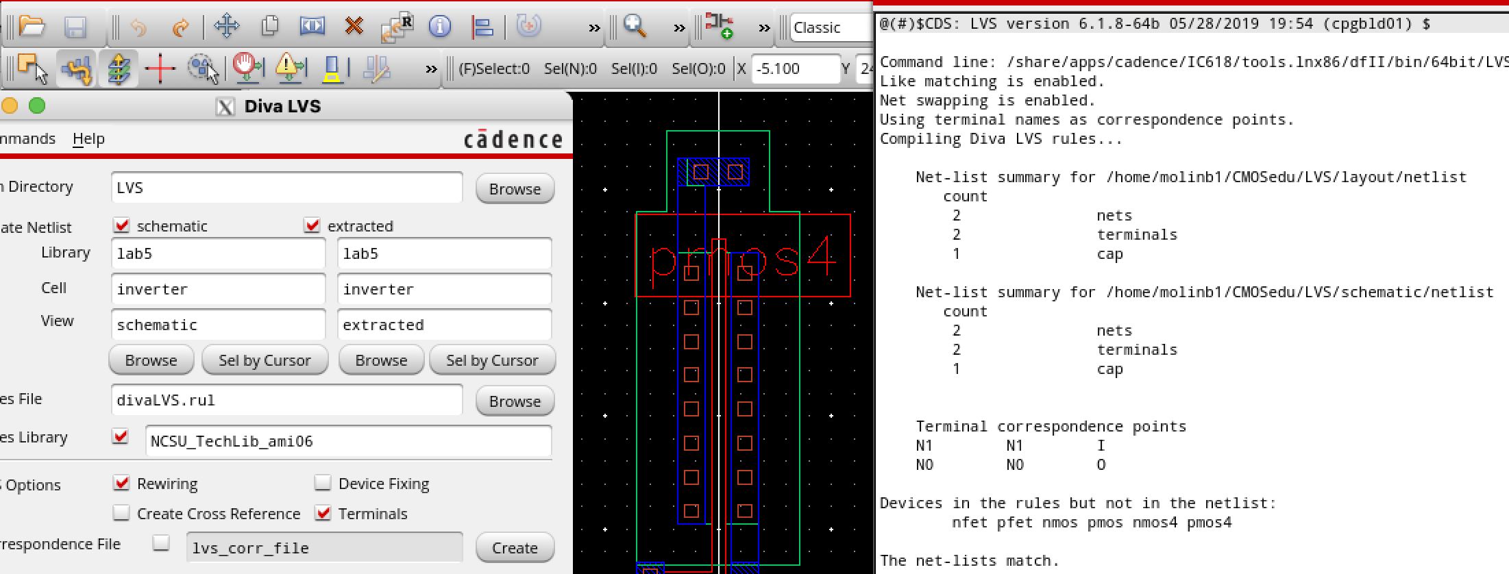
Here we can see that they clearly do match and we can proceed onto the next part fo the lab.
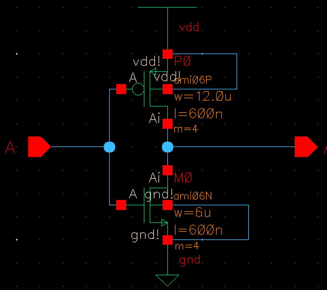
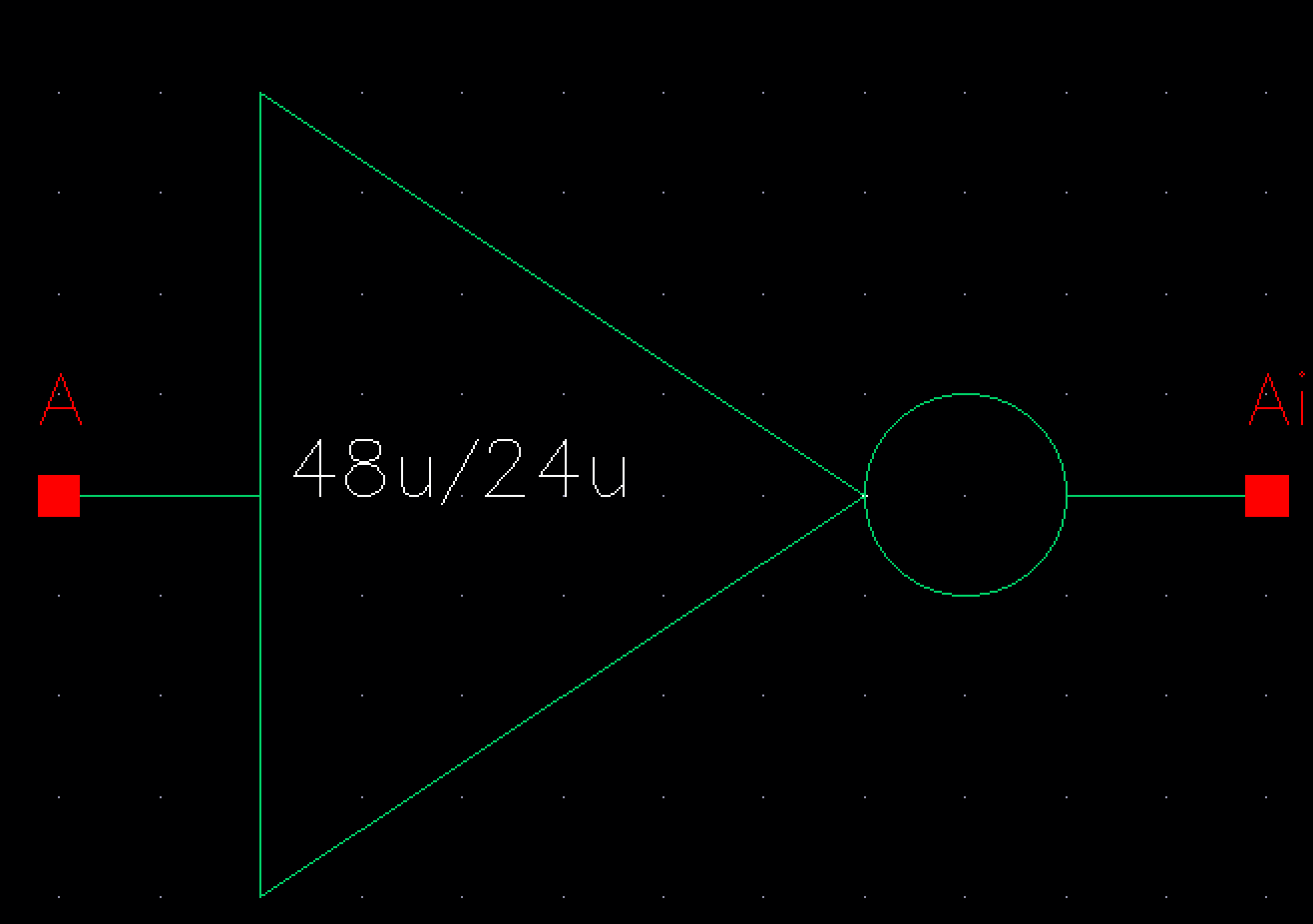
Creation of a 48u/24u Inverter:
Now
we want to make an inverter with a 48u/24u ratio. However it is
impractical to make MOSFETs that long in practice. So what we do
instead is increase the multiplier on the MOSFETs to make it equivalent
to one of that size. So we make the multiplier on both the PMOS and
NMOS m = 4, since 12u * 4 = 48u and 6u * 4 = 24u respectively.
Increasing the multiplier will add more fingers to the MOSFET meaning
we have to change the wiring of metal1 a bit in the layout but the
principle remains the same.
As before a schematic, symbol, layout and extracted view must be made.
| 48u/24u Inverter Schematic | 48u/24u Inverter Symbol | 48u/24u Inverter Layout | 48u/24u Inverter Extracted View |
 |  | 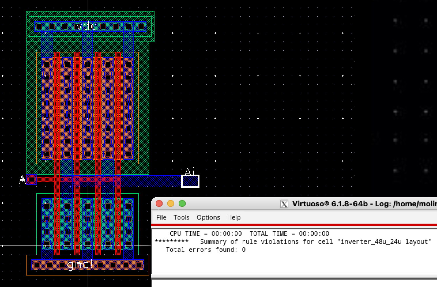 |  |
Now as always we LVS the extracted view and the schematic to make sure that the netlists match up.
Ultrasim simulations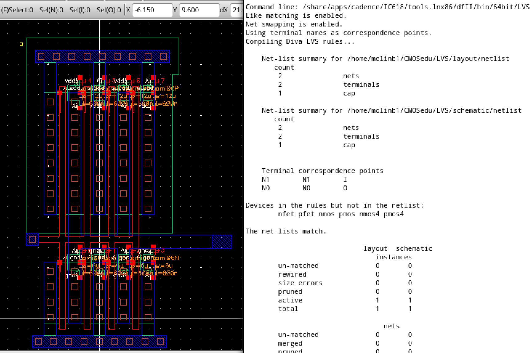
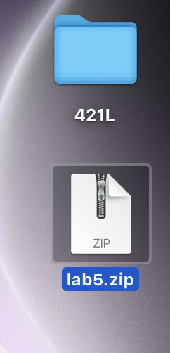
The
files for all that was created up to this point in this lab were saved
and zipped up and saved. There are also contained here at lab5.zip.
Simulations of 12u/6u Inverter by Driving Capacitence Loads:
Now
we wish to see how the inverters respond to having varying capacitances
as loads. Remember that capacitors resist changes in voltages that
occur in circuits, so the stronger they get the more we expect to see
the output waveform change and smoothen out.
We normally just use
spectre for our simulations but here we will also use Ultrasim to see
varying results. Ultra tends to run faster but often has inaccuracies
because of this speed.
| Capacitance | Spectre simulations | Ultrasim simulations |
| 100fF | 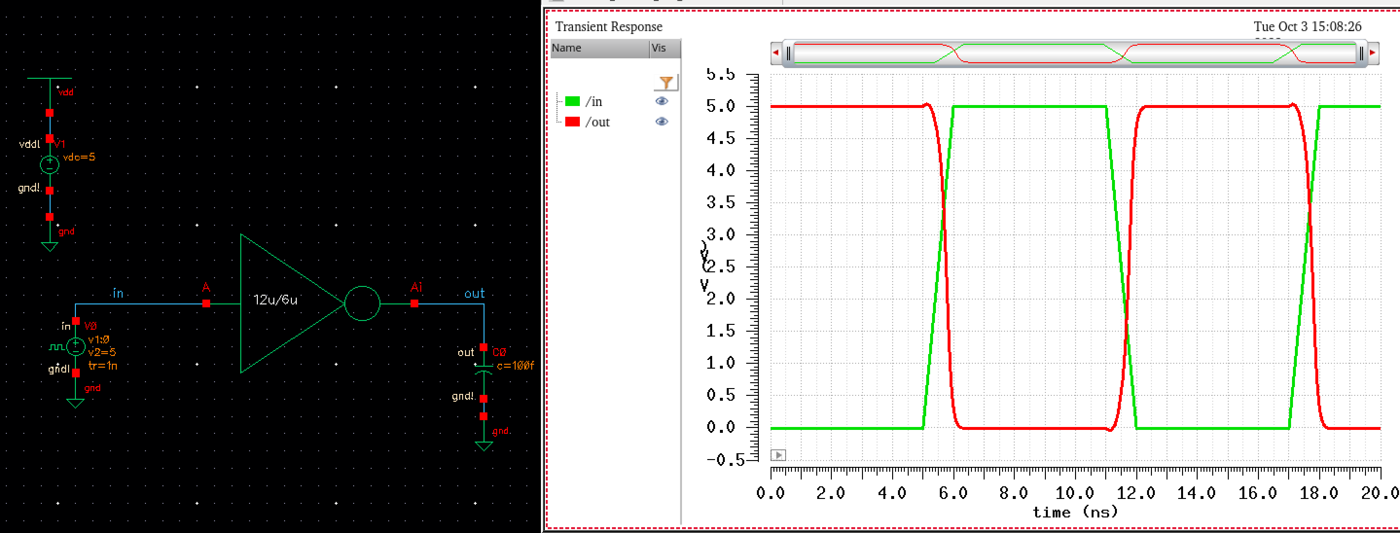 | 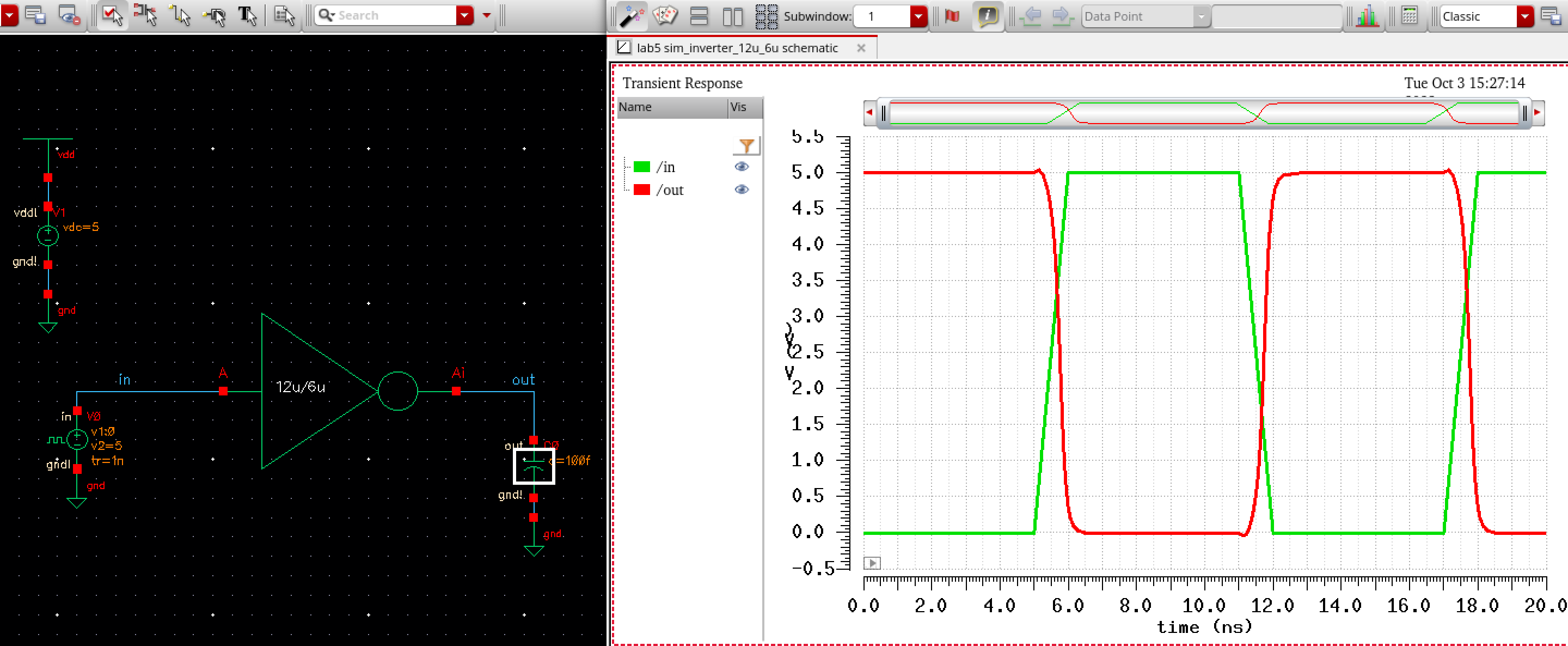 |
| 1pF | 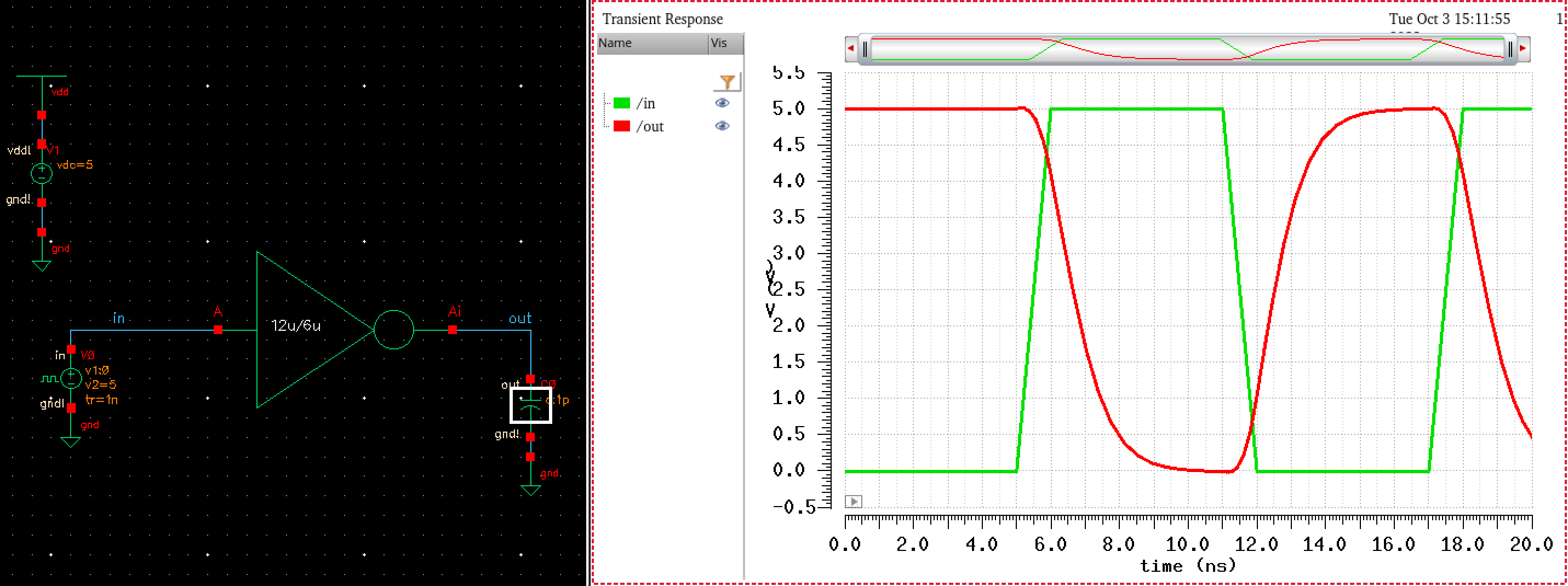 | 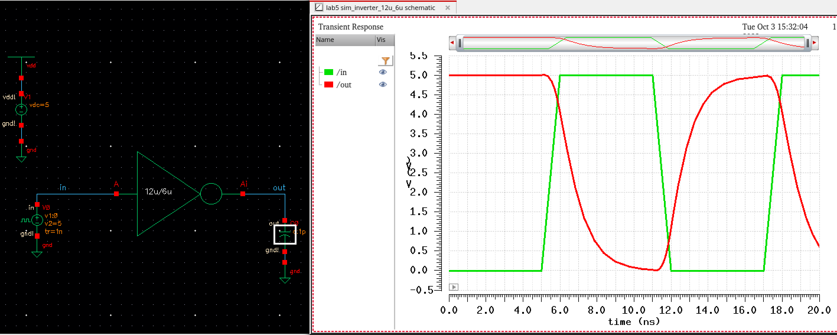 |
| 10pF | 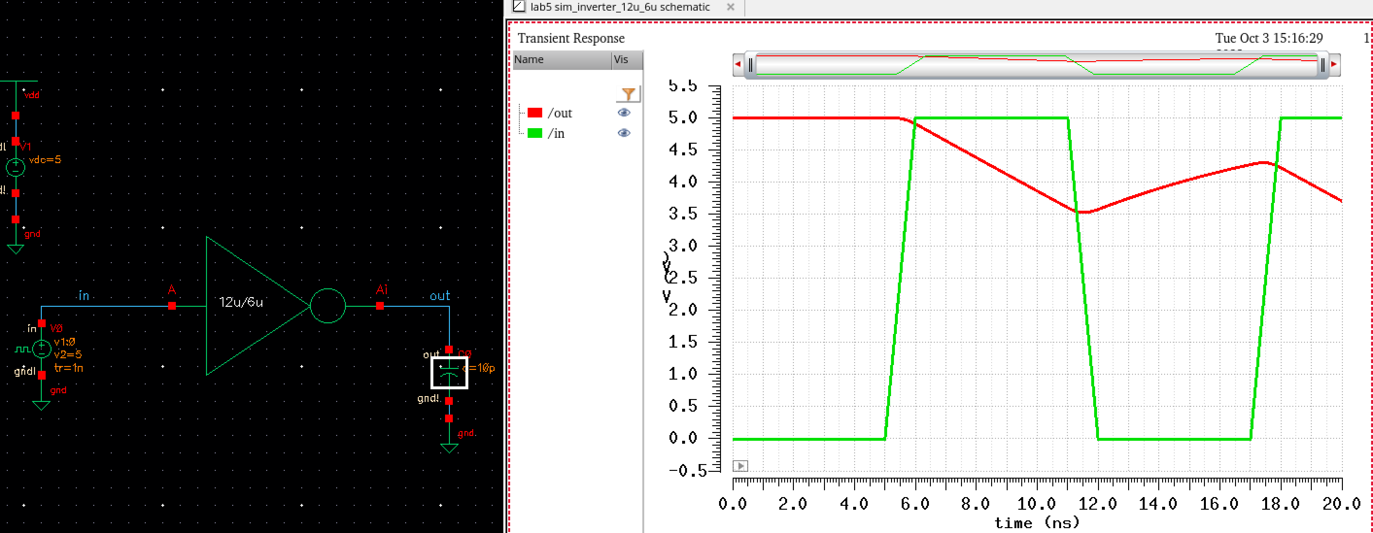 | 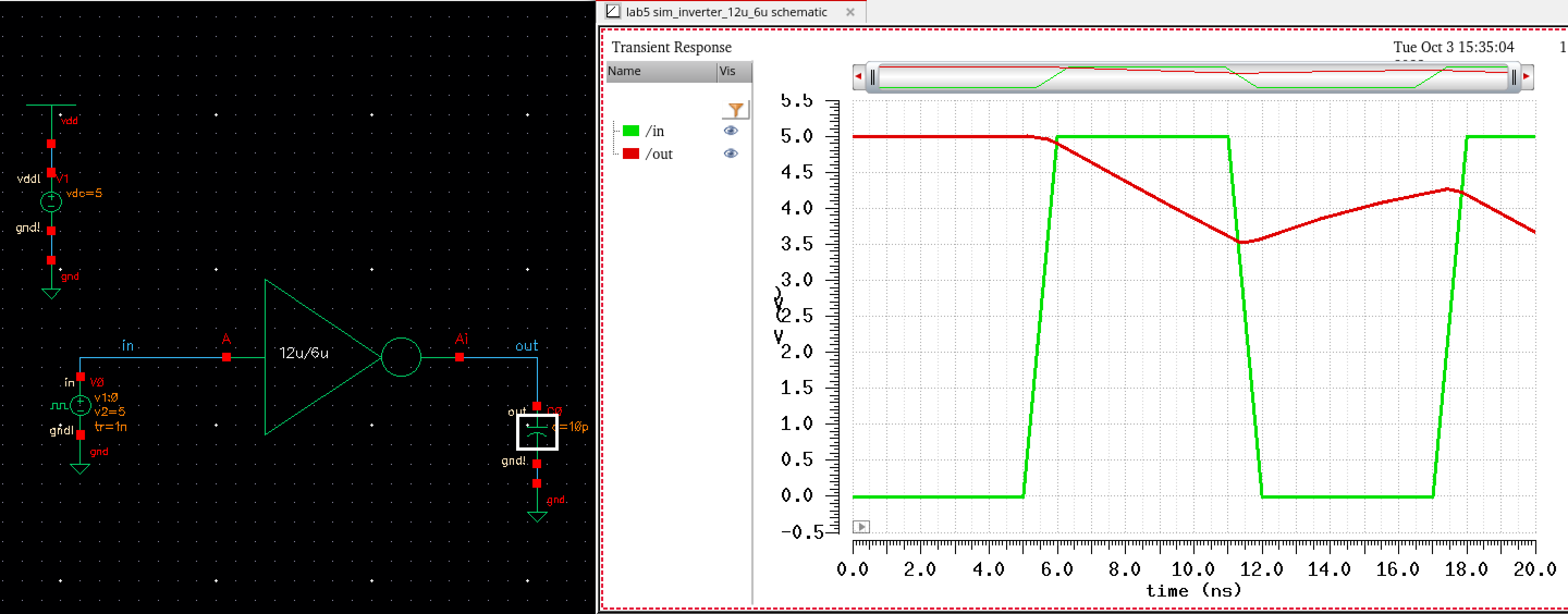 |
| 100pF | 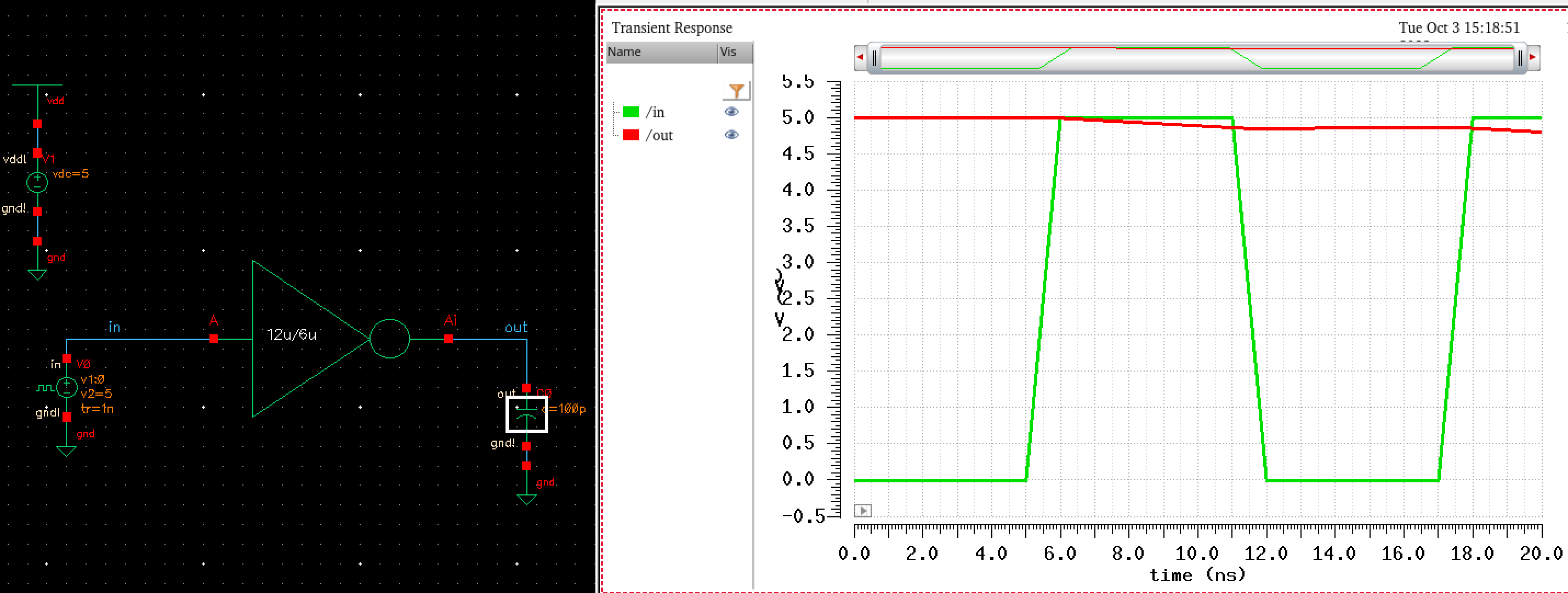 | 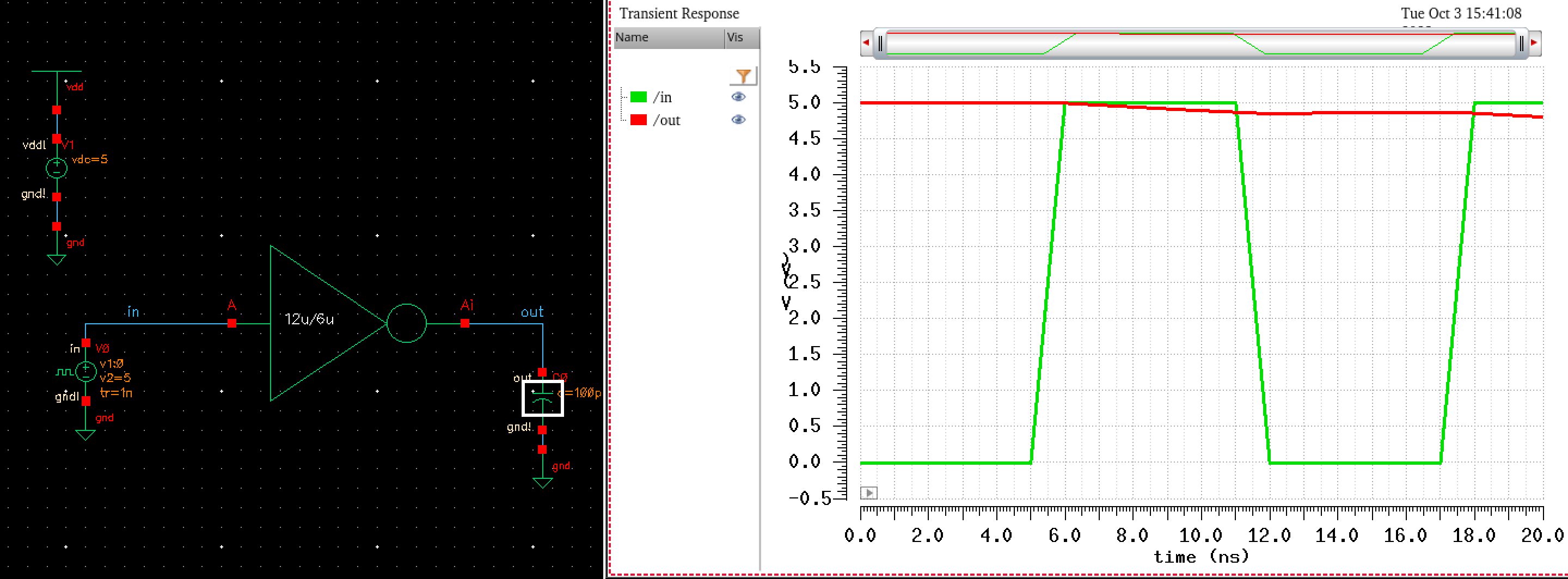 |
From
these images it becomes clear that the larger the capacitor gets the
smaller the output wavefrom gets. This is because the greater
capacitance means it takes longer and longer for the capacitor to
charge when having the input signal go through it. Effectively
smoothing out the output waveform.
Simulations of 48u/24u Inverter by Driving Capacitence Loads:
As we just did with the 12u/6u we will now drive loads of capacitance to the 48u/24u inverter and see what happens.
| Capacitance | Spectre simulations | Ultrasim simulations |
| 100fF | 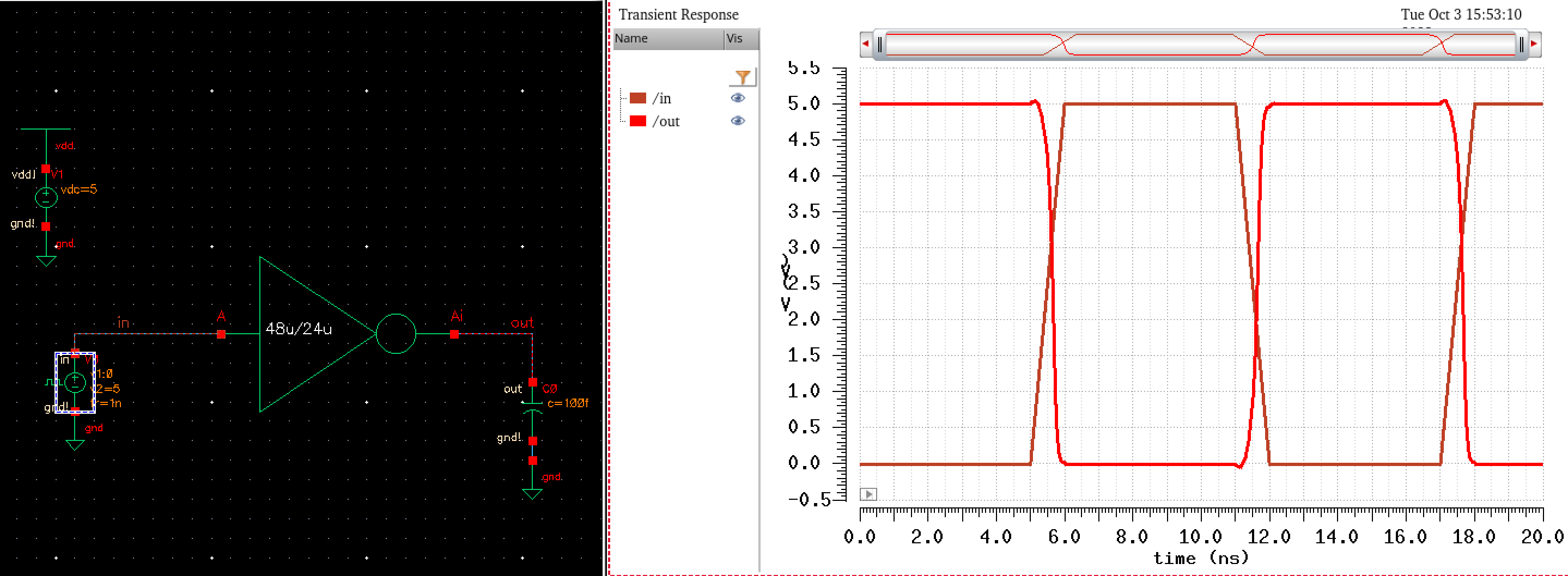 | 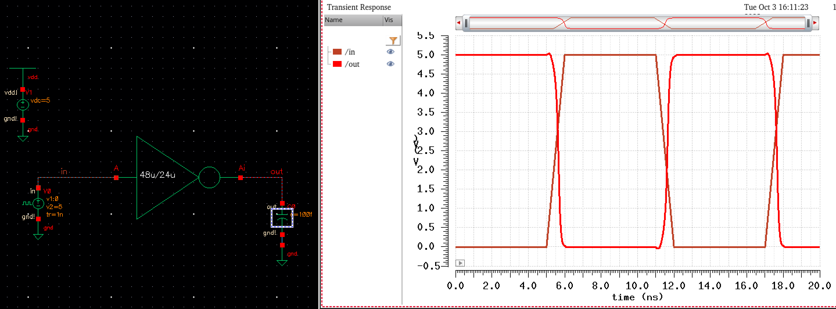 |
| 1pF | 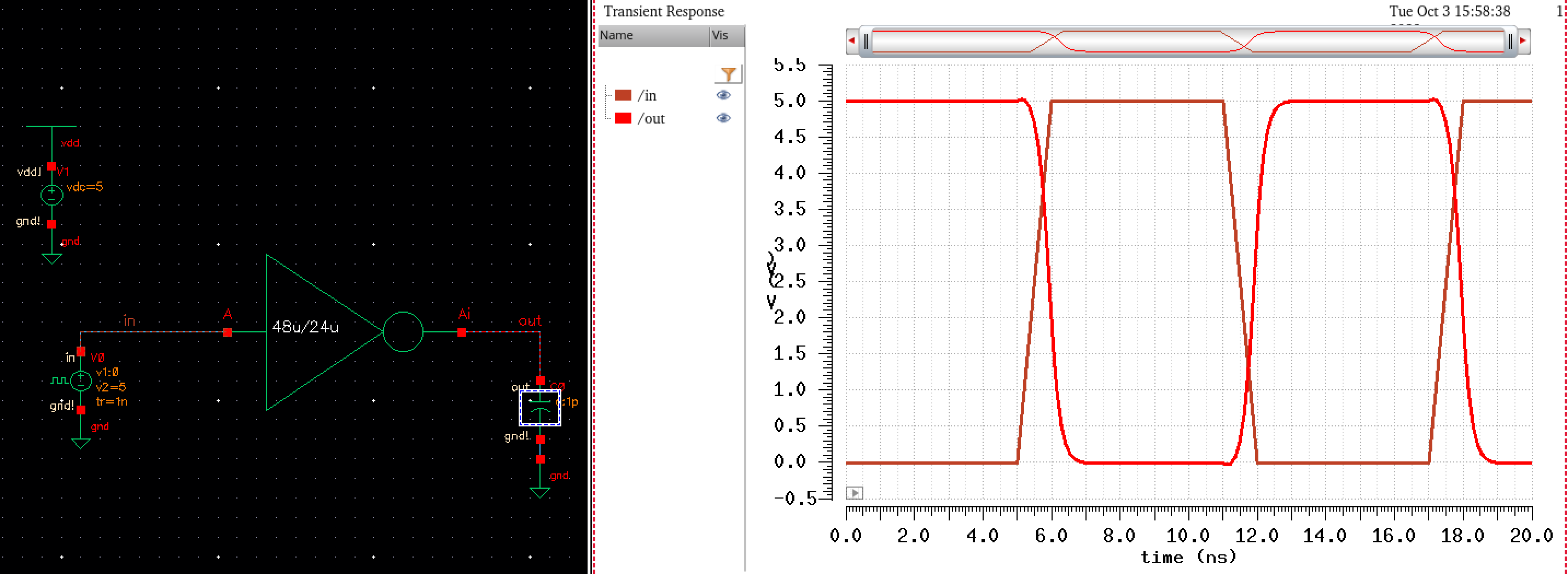 | 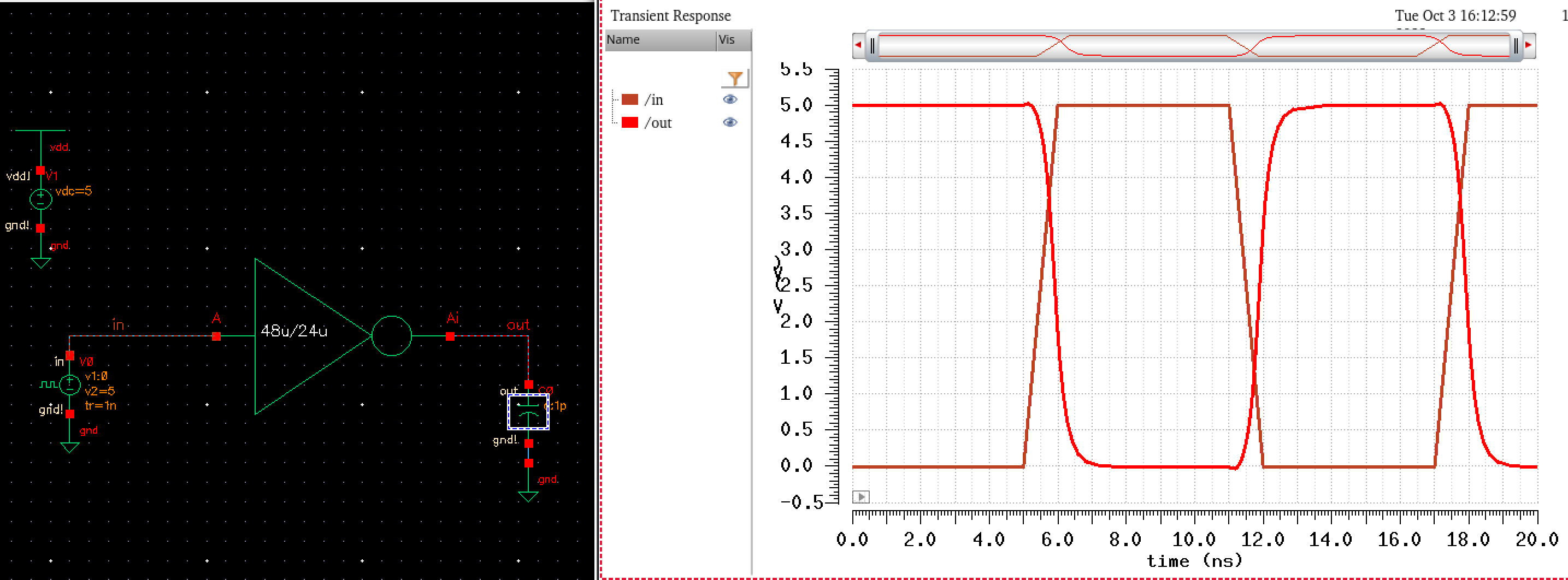 |
| 10pF | 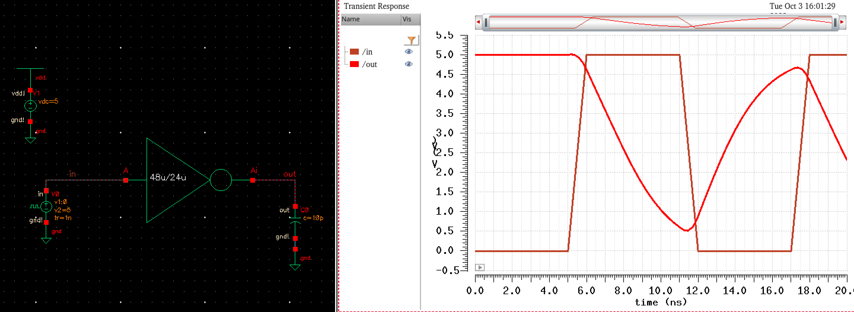 | 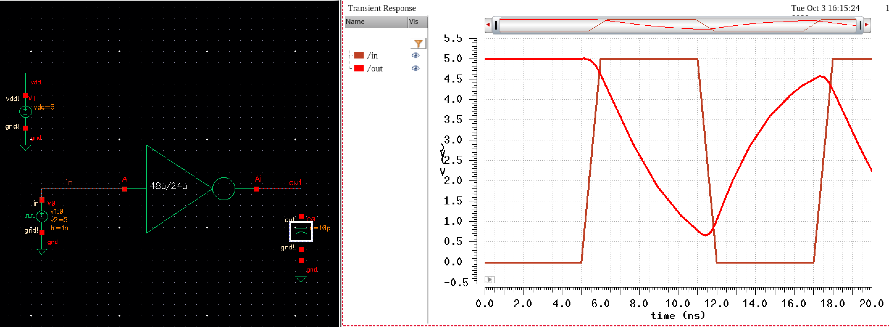 |
| 100pF | 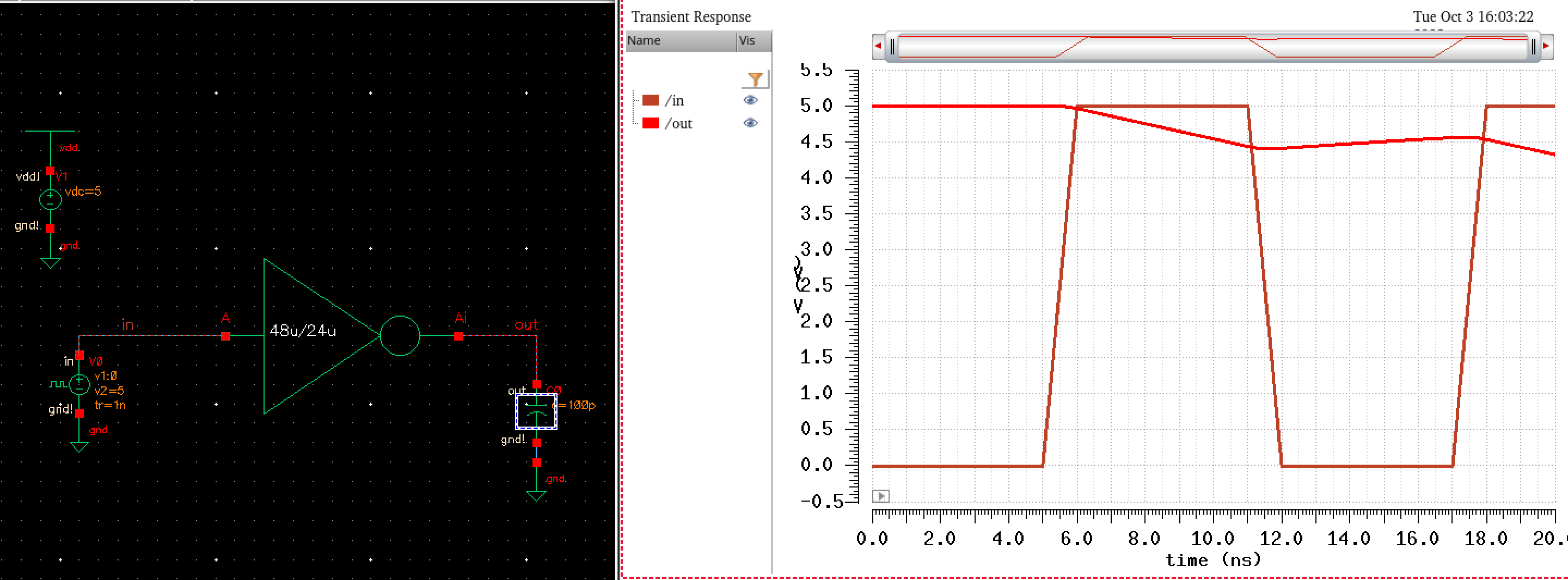 | 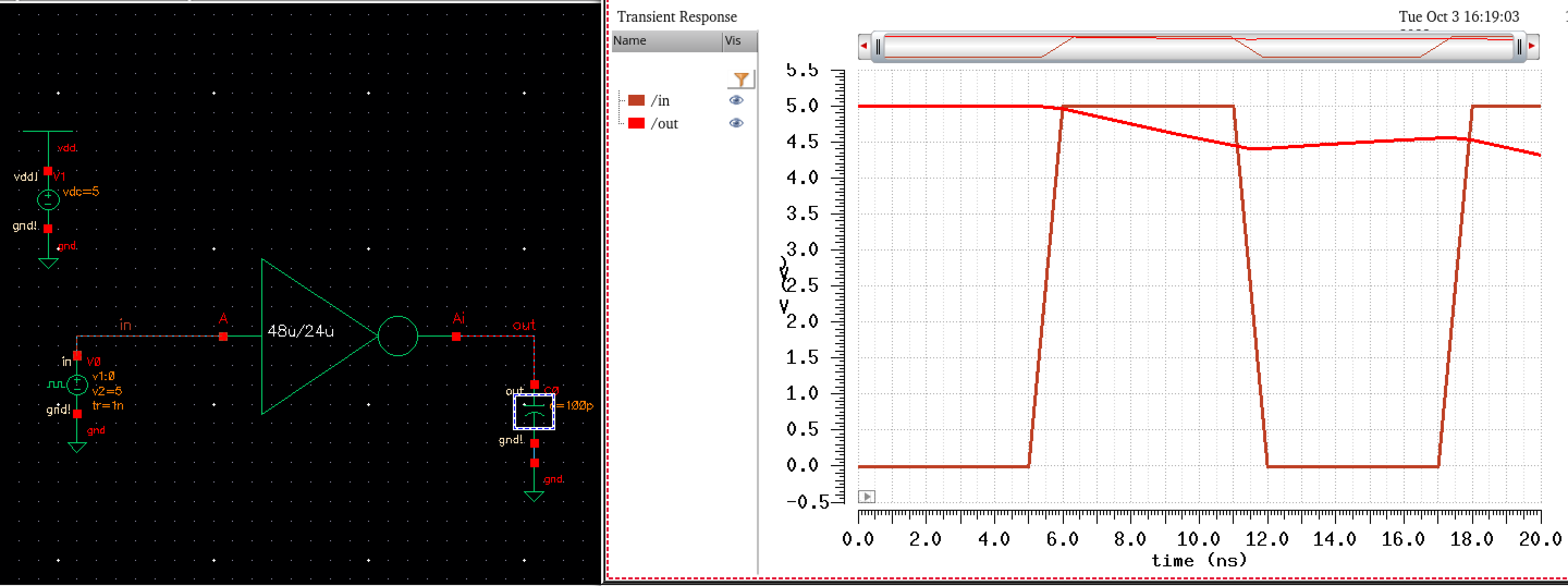 |
From
these results we can conclude that an inverter with a bigger ratio of
the PMOS and NMOS sizes has an easier time resisting the effects of
higher capacitance values than an inverter made with an NMOS and a PMOS
that has a smaller ratio between their sizes.
We can also see a
small difference between the spectre and the Ultrasim simulations.
Which does seem to conclude that Ultrasim is less accurate. However for
this lab Ultrasim actually ran slower than spectre did. This may simply
due to my internet connection that I use to connect to the Candence
server rather than the software itself. But it still felt like that
discrepancy should have been noted.
As always all work is saved and backed up on laptops and google drive just in case.

Return to EE421L Labs