Lab 4 - ECE 421L
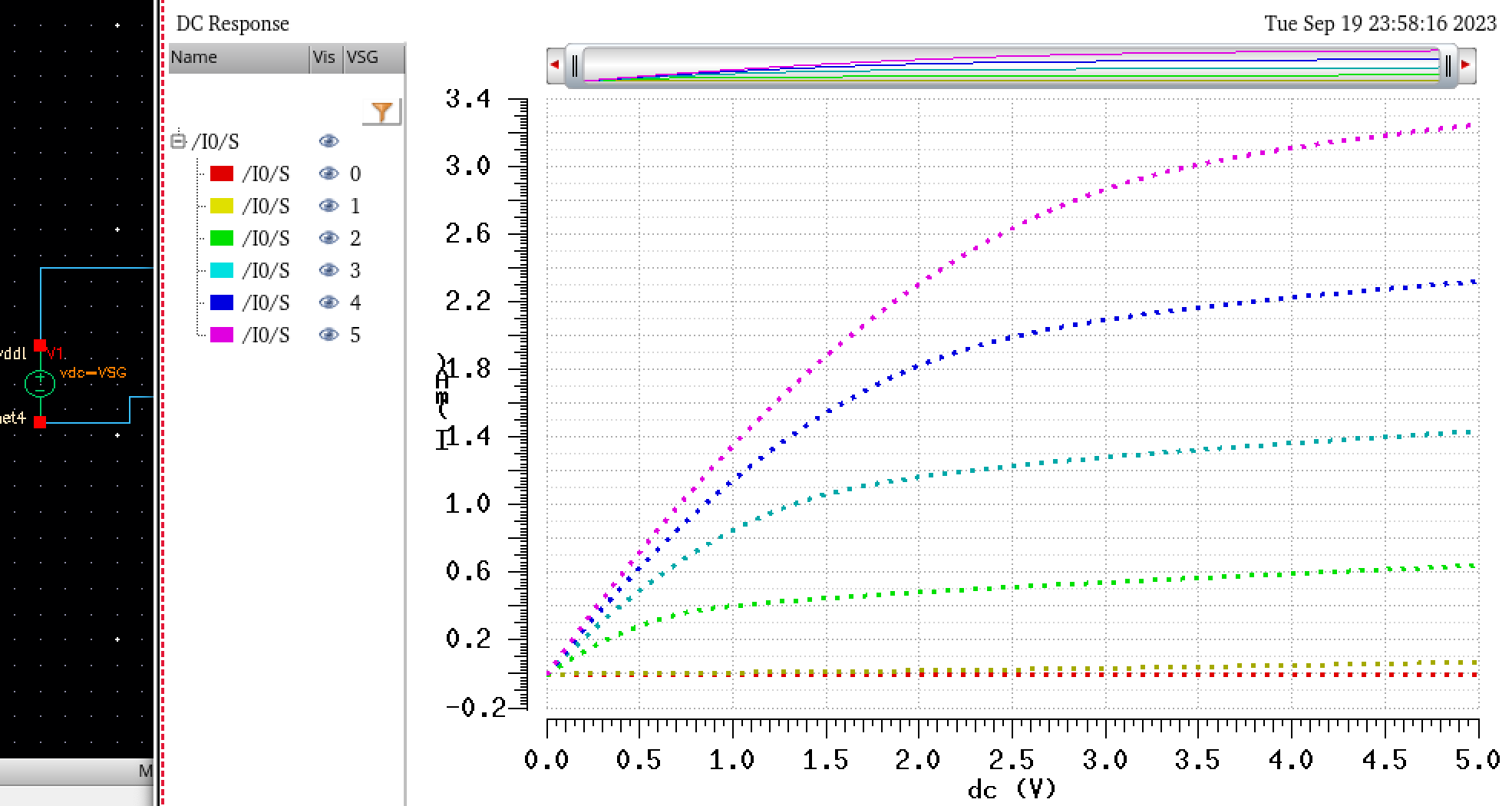
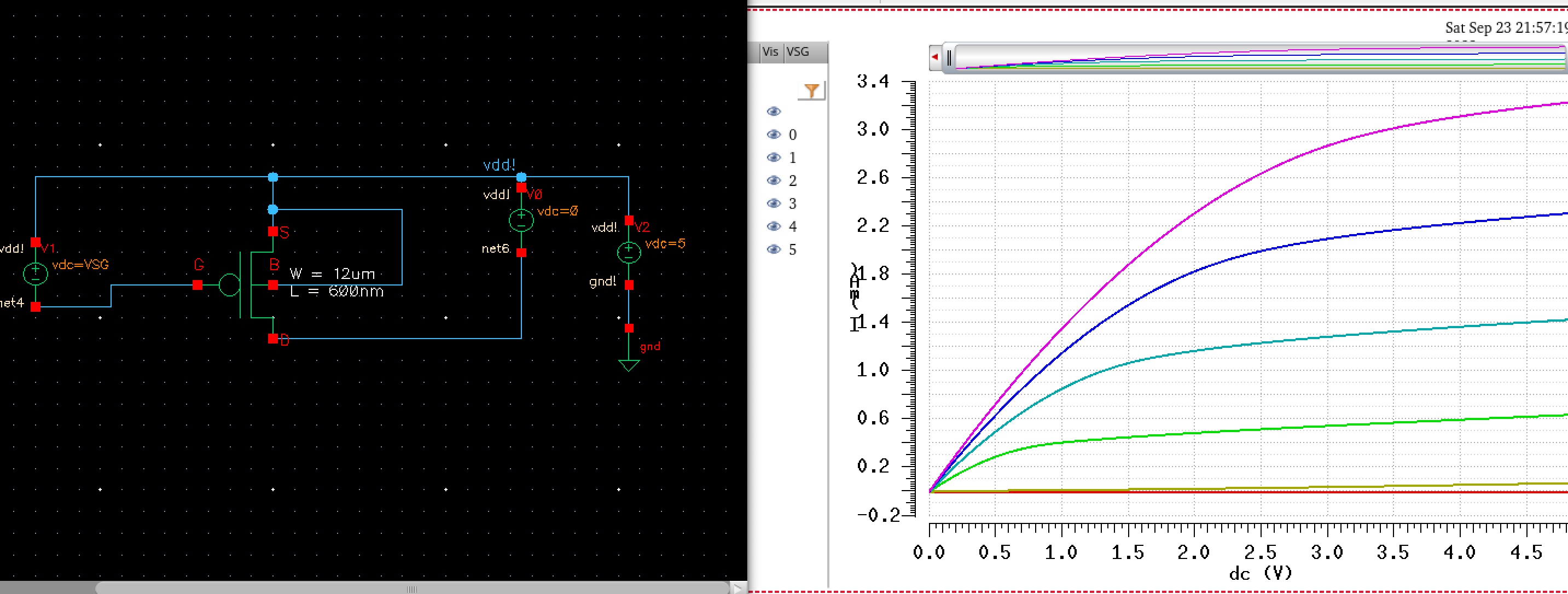
Simulation #4: ID v. VSG of a PMOS device for VSD = 100 mV where VSG varies from 0 to 2 V in 1 mV steps.
The next step we must perform will involve creating a layout with these NMOS and PMOS devices and combining them with a probe pad which are smaller than probe pads. Be sure to look at MOSIS if you are confused about the design rules for these pads. All they are, is a simple "glass" layer over a bigger "metal3" layer.
NMOS:
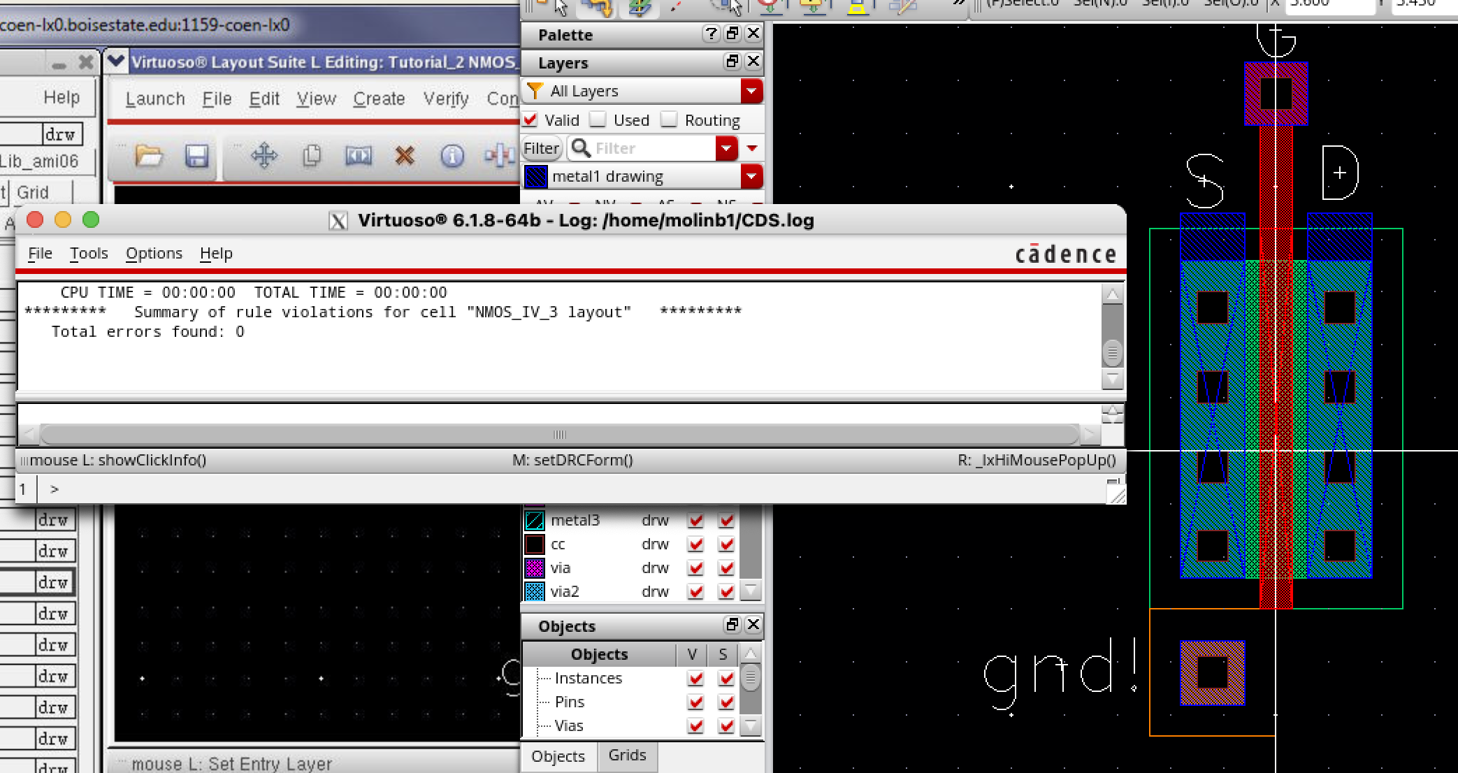
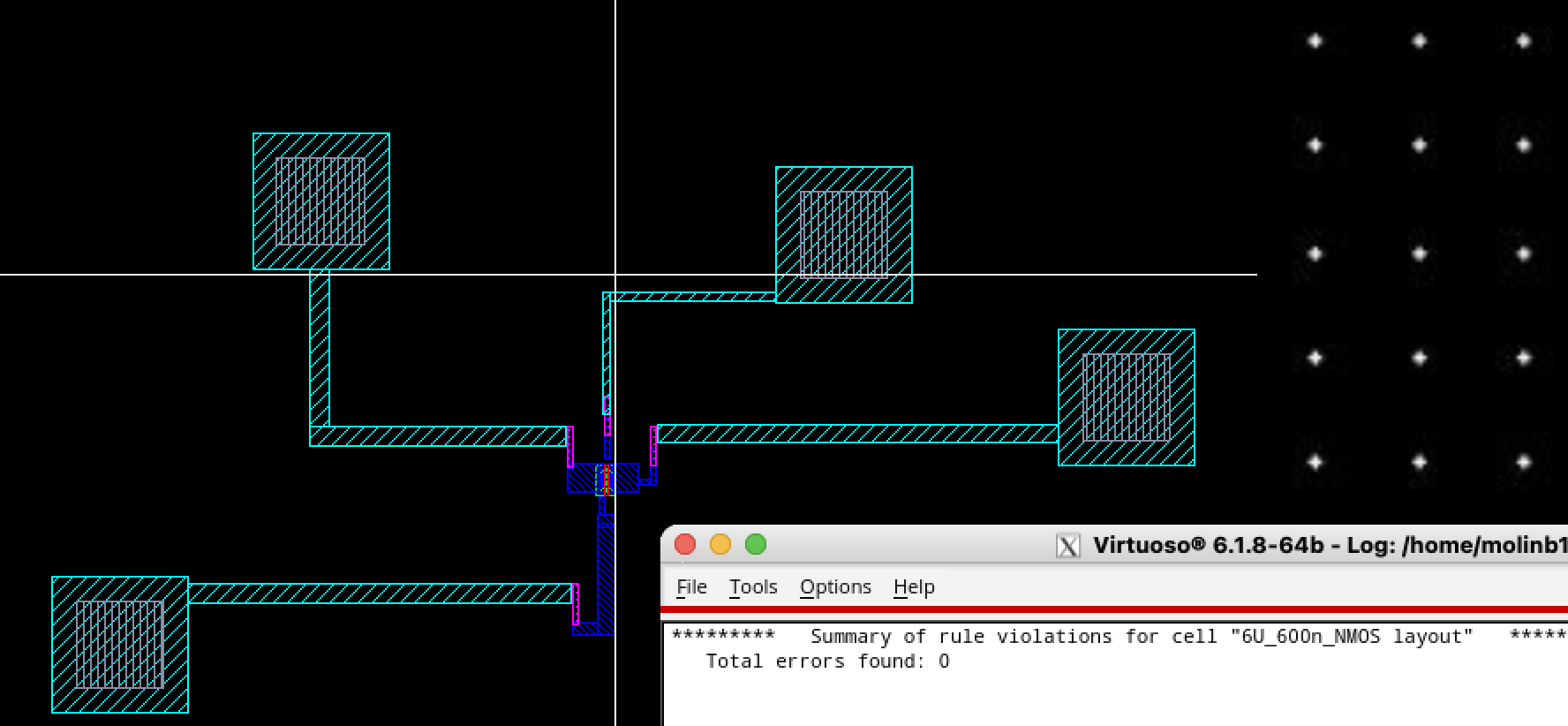
Below we see the layout created with the pads and the NMOS that is based on the examples provived by Dr. Baker, as always we DRC this design to make sure all is in order and spaced out evenly. When you get zero errors extracted this layout for later use.
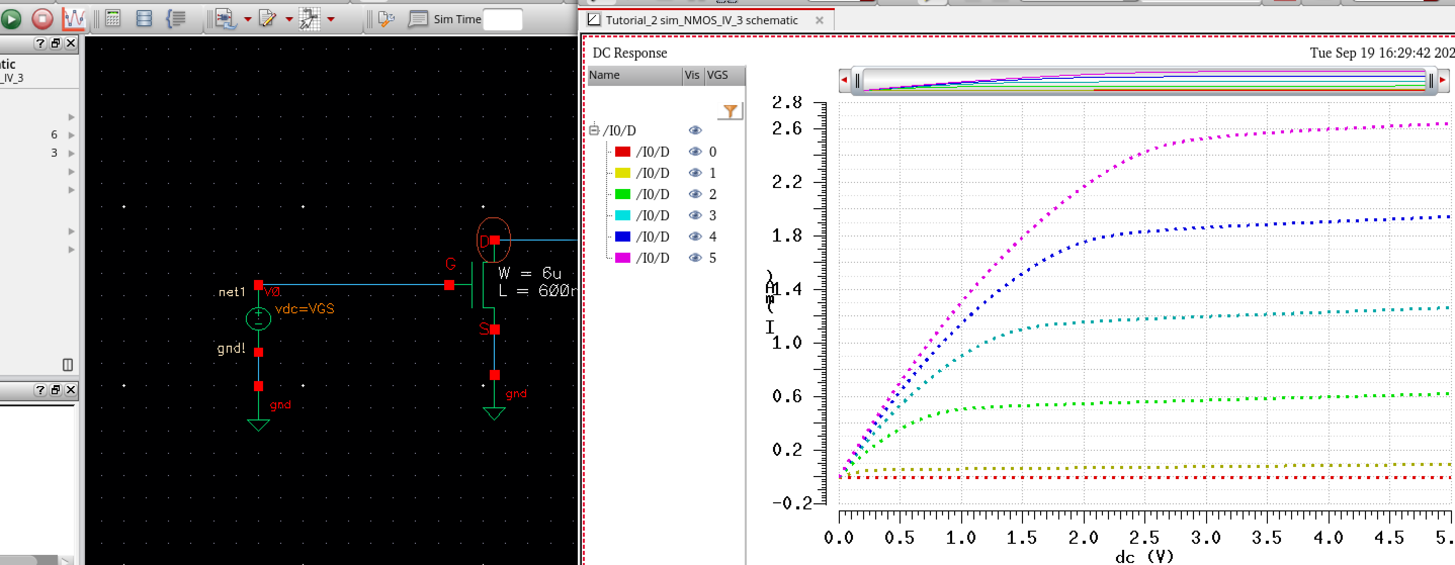
We now make a schematic with the probe pad symbols for the NMOS noting that the Body pin that we normally use is simply gnd!.
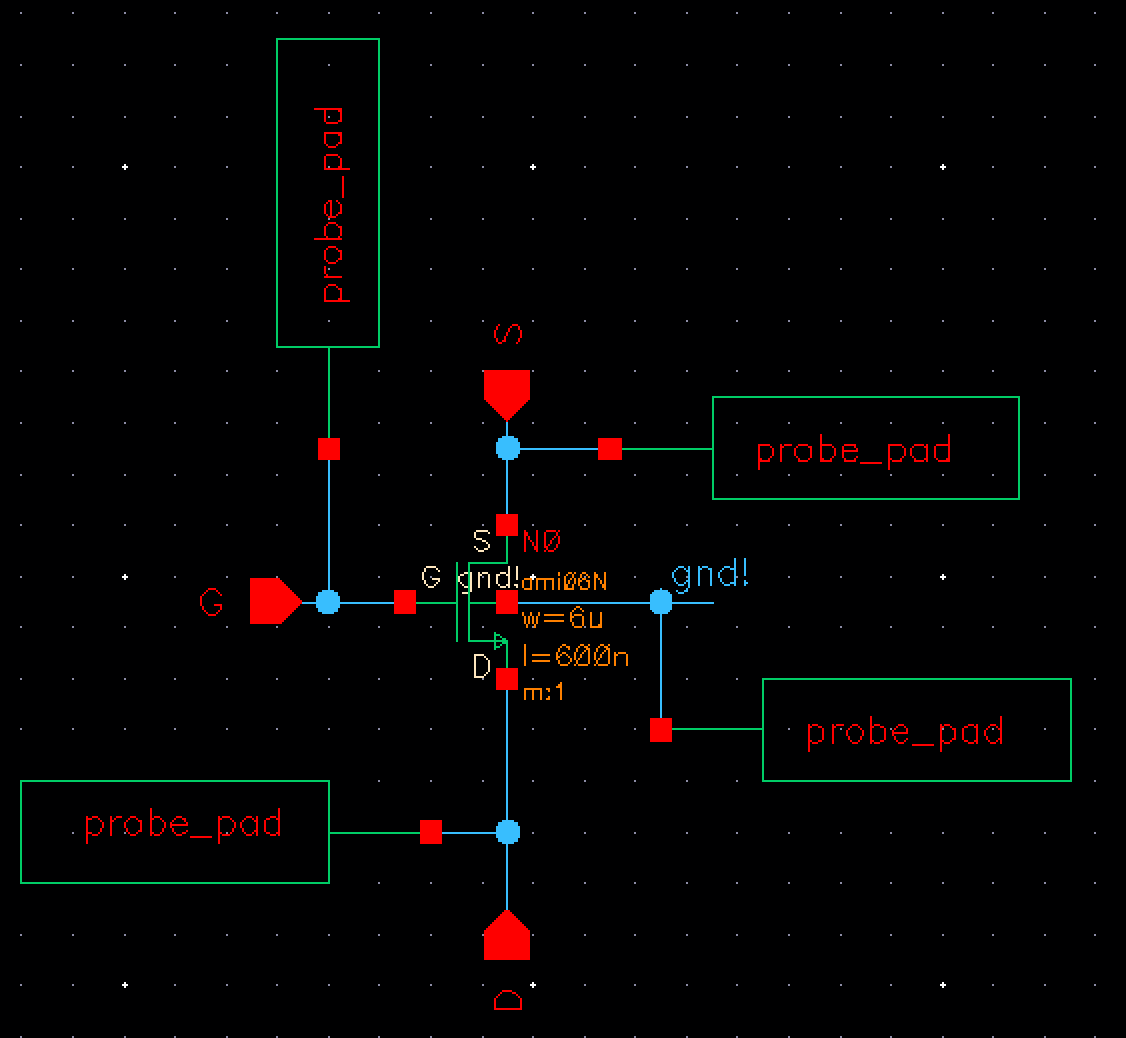
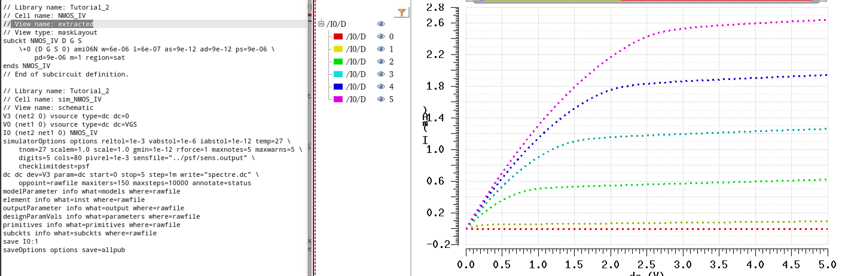
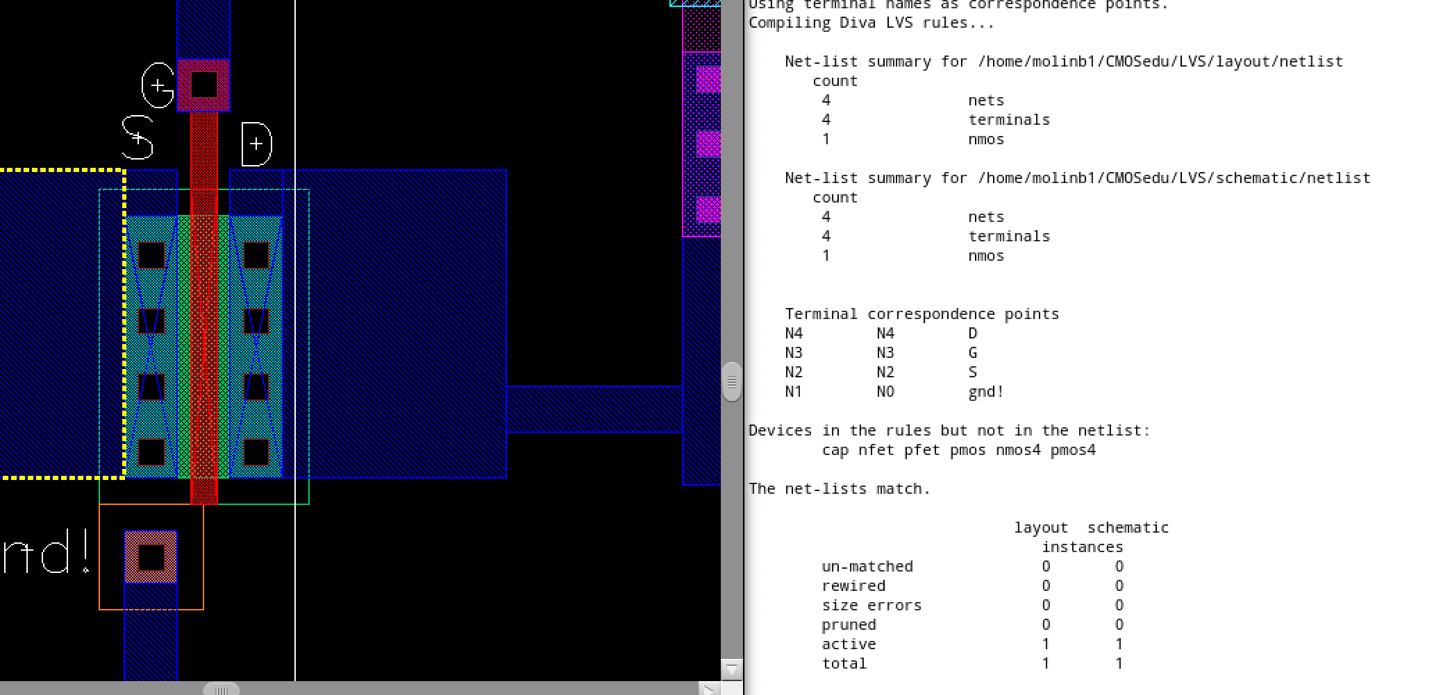
Then all we need do is LVS using the schematic and the extracted view we made earlier. Here we can see that the netlists match and I have included a zoomed in view of the NMOS device and how it is connected to the pads.
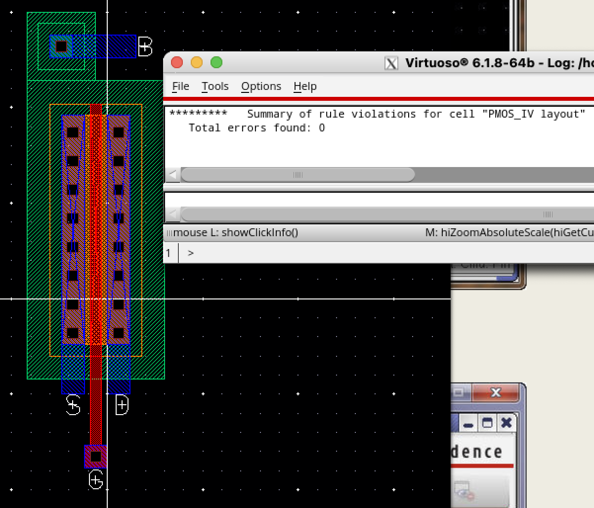
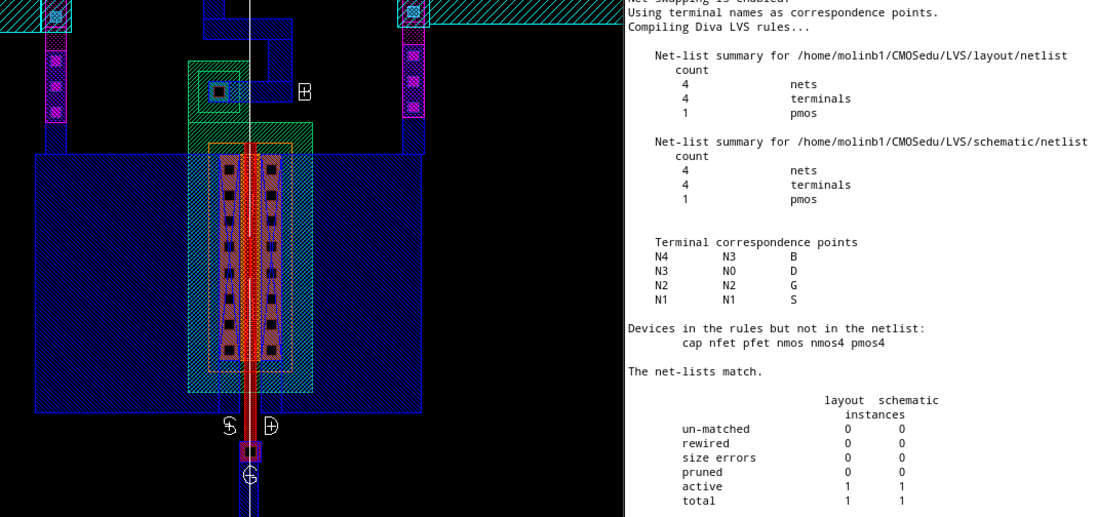
PMOS:
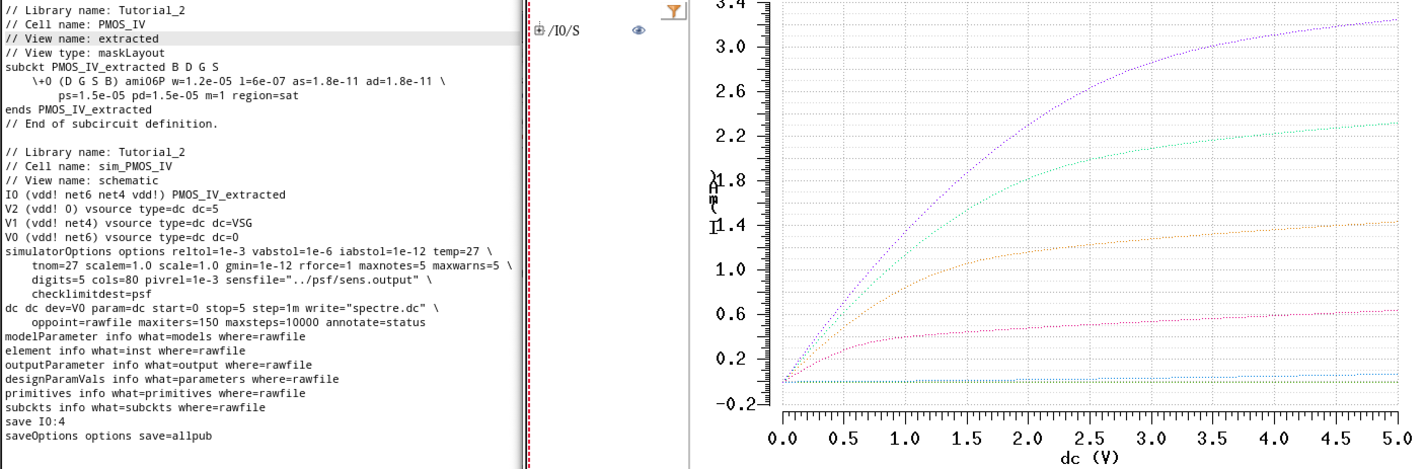
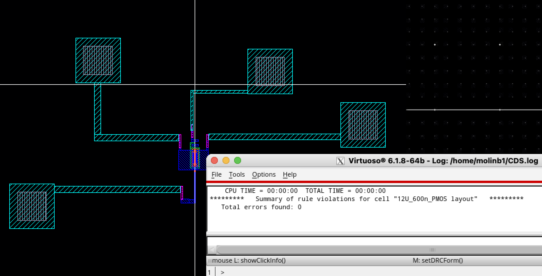
Just as before with the NMOS we now must do the same thing with teh 12u/600n PMOS that we have built. Once again using DRC to check when we finish designing. Extract when given zero errors.
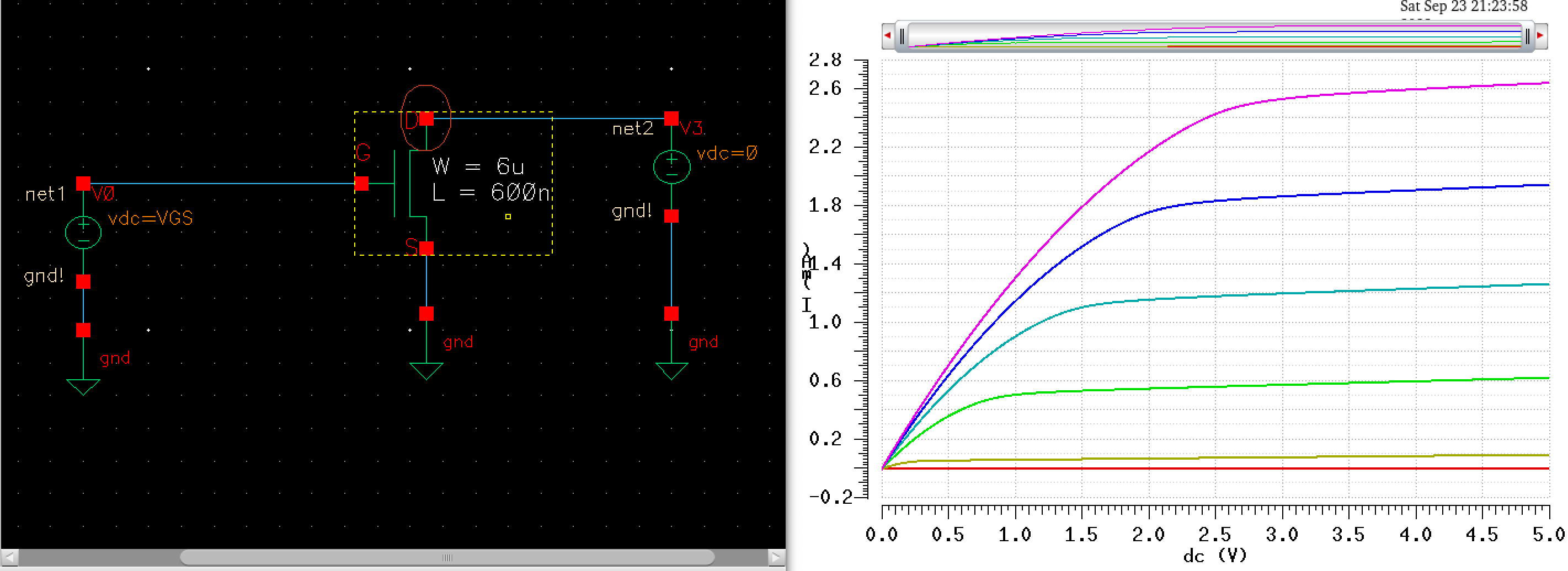
The schematic for the PMOS design this time using the Body pin and connecting it.
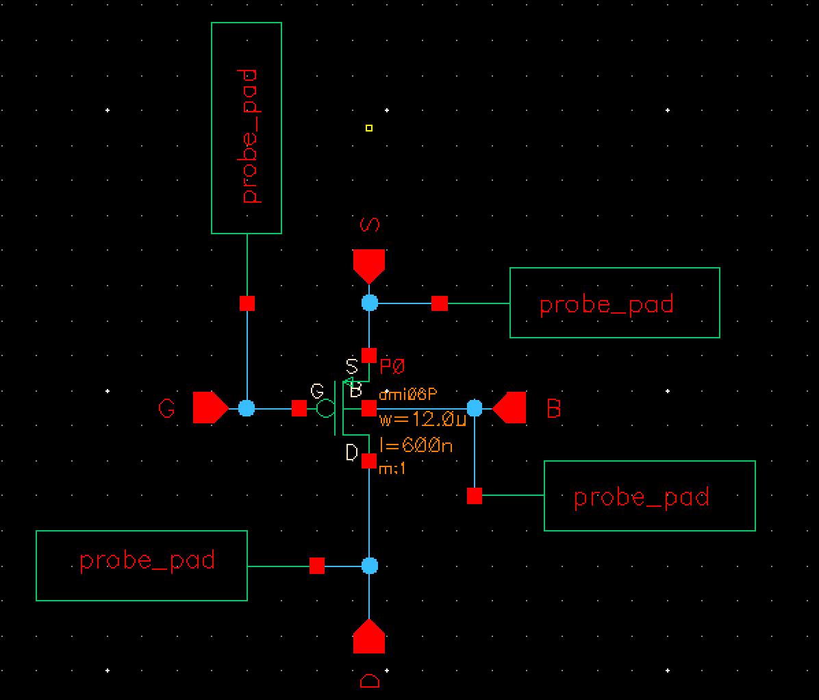
And finally we LVS the schematic and the extracted view and if done correctly the two netlists must match. Once again for convience I have zoomed in on the PMOS device to show how it connected to the pads in the layout.
Proof of backing up and saving work:
Work was zipped and sent to google drive as a backup and extra save.