Lab 3 - ECE 421L
Zipped Up Lab 3:
Prelab:
The prelab for this lab merely backing up and saving your work from the last labs. Here I will show a few images to prove the validity of the components I built for this lab.
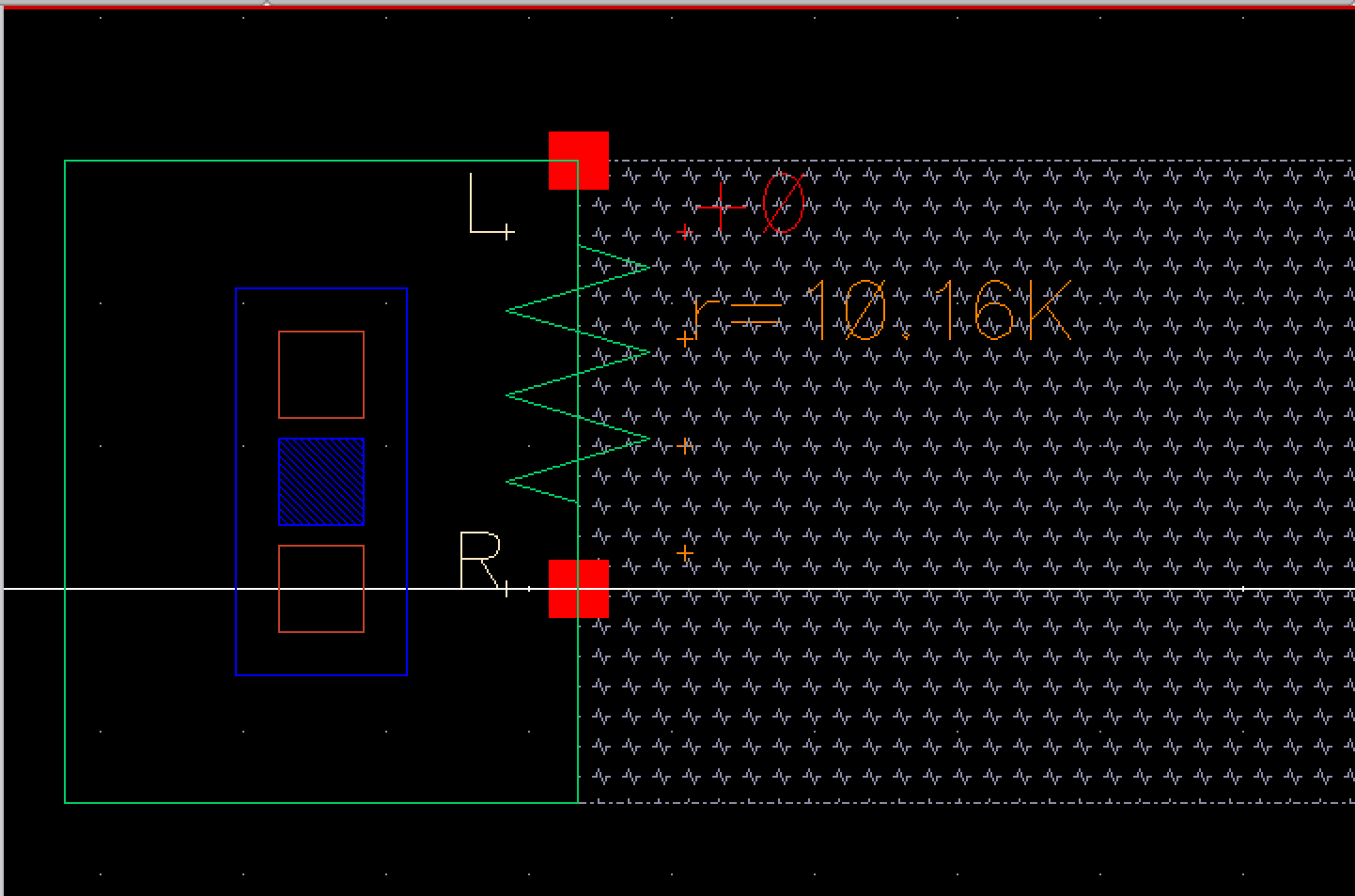
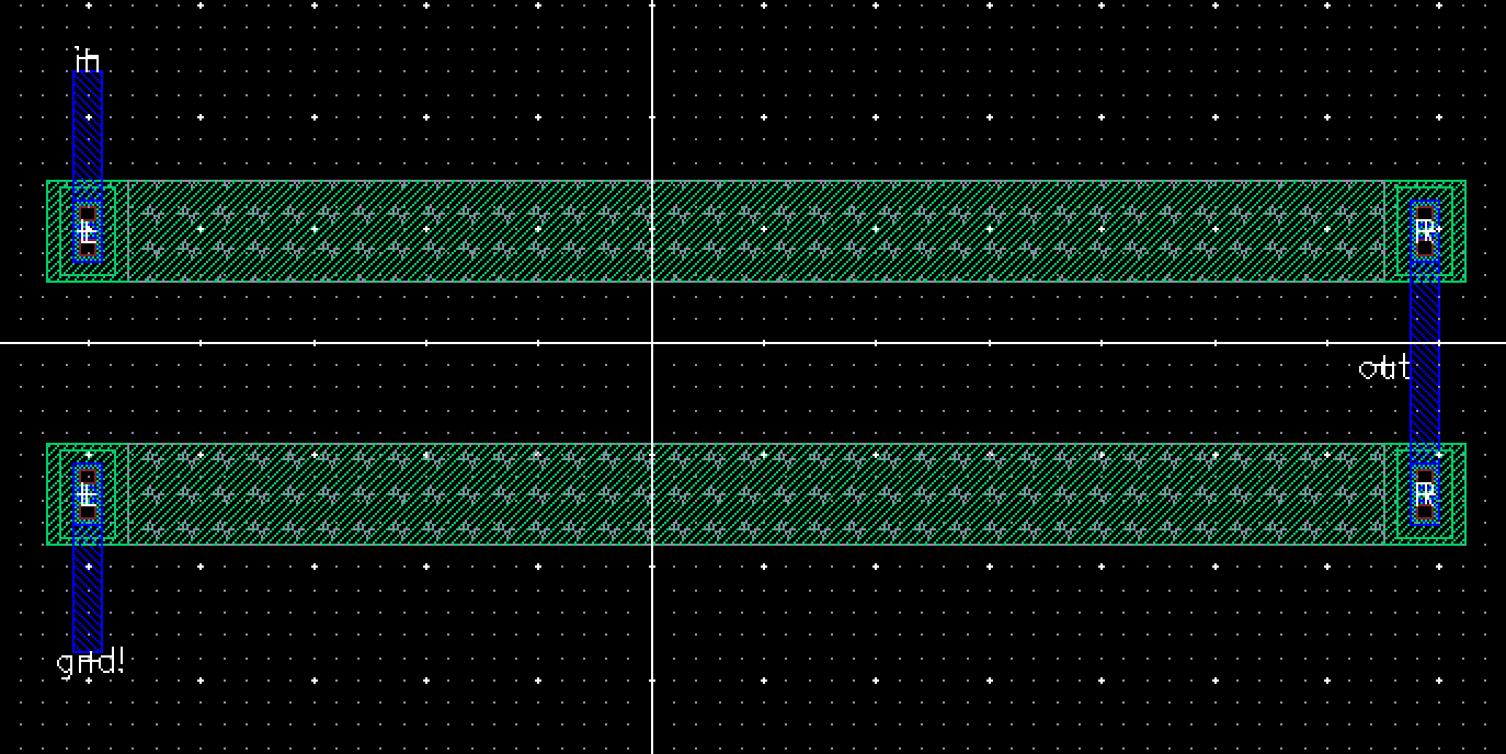
Below is proof that the n-well that was designed was at least 10k in value.
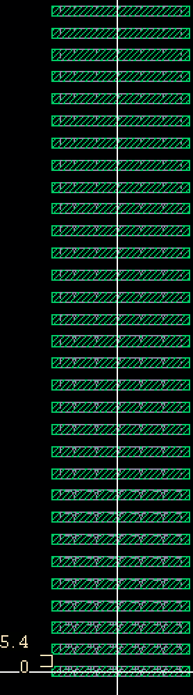
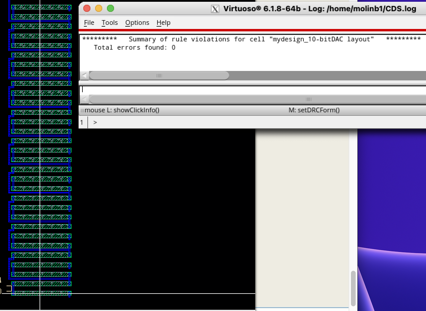
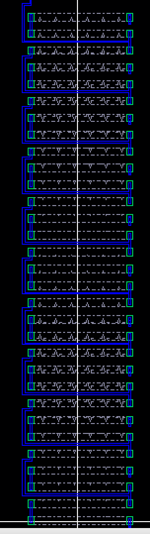
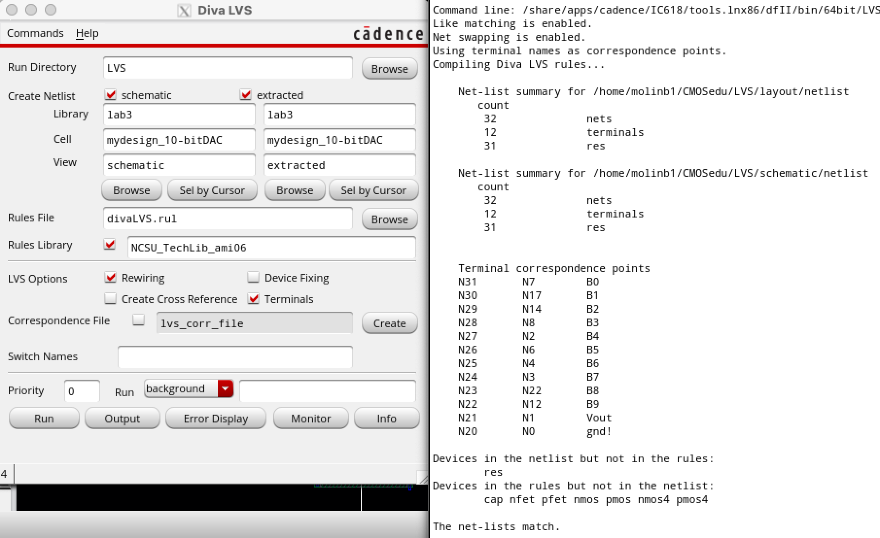
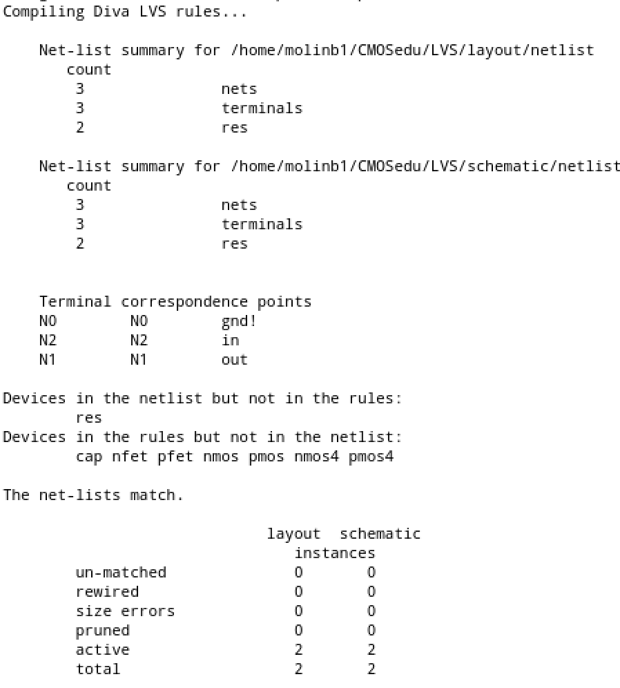
These images below show the layout of the voltage divider the is designed with these 10k n-wells then proof that the netlist of this and the schematic of a 10k voltage divider match up.
Now that we have all of those in order the next step is to create a new directory called lab3. I did this by copying the lab2 directory and renaming the copy to lab3. This makes sense since a majority of the work we need is from this library. We merely copy the n-well layout and schemtic for the voltage divider into the lab3 library as well.
Lab Procedure:
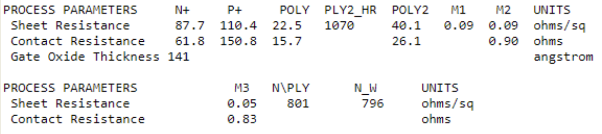
First we wish to check the MOSIS parameter files and see what we have for the sheet resistance. Which is about 796 ohms/sq according to the image below.
Using this knowledge we can do some calculations, but first we need the length and the width of the N-well I designed.
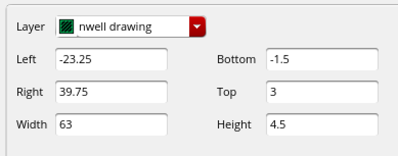
Most people used the minimal value of the n-well which was 12 lambda which ends up being 3.6um. I used 4.5um to make the n-taps fit better, all this means is that my width will have to change to accomadate this.
The formula for R is as follows R = Rsq * l/w. So if we want to calculate a reasonble width for a 10k resistor we can calculate this.
l = (10k * 4.5u)/796 = 56.5um
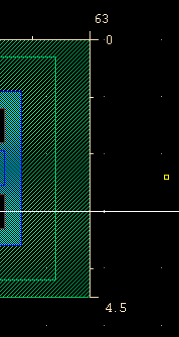
We need this value to be a multiple of lambda and I increased it to a value of 63um since I put the n-taps within the n-well rectangle so that decreased the length between them. In the end I get 10.16k which is reasonably close meaning the final length between the n-taps should be around the calculated 56.5um but also a multiple of lambda.