Lab 2 - ECE 421L
To start students were asked to download the lab2.zip file and input it into the directory and unzip it.
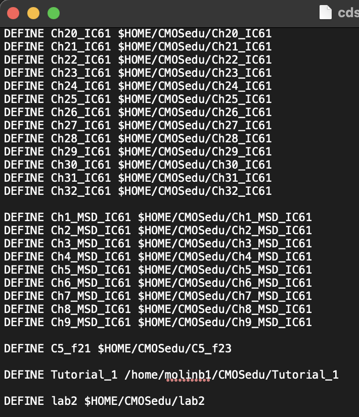
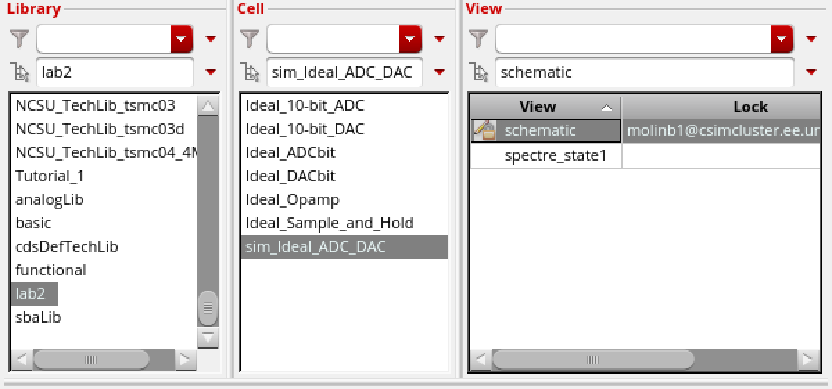
As always we must define our new file in the cds.lib file by adding "DEFINE lab2 $HOME/CMOSedu/lab2".
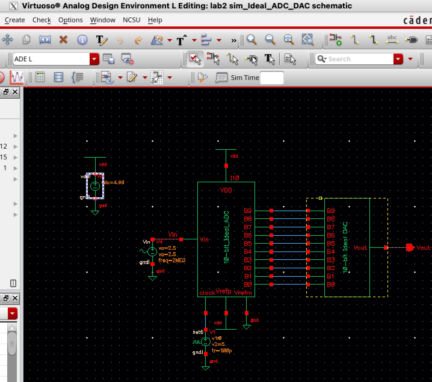
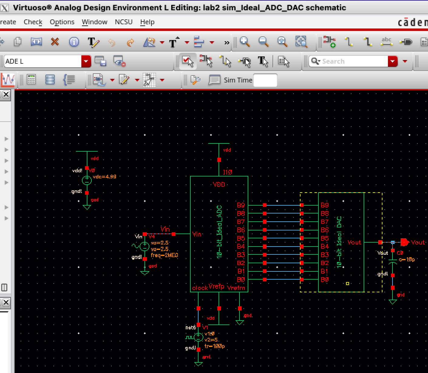
Now we can open Cadence and open the sim_ideal_ADC_DAC cell. Specifically the schematic view. You should get the image presented below.
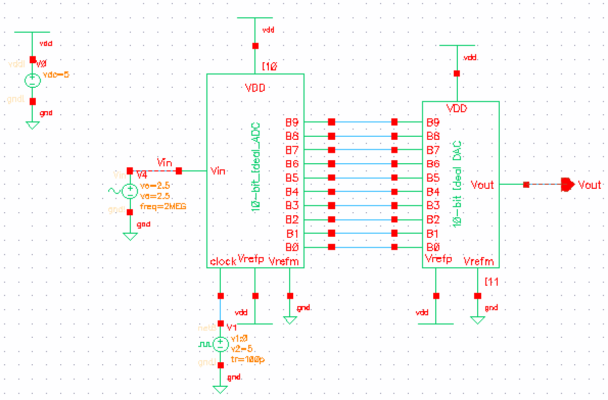
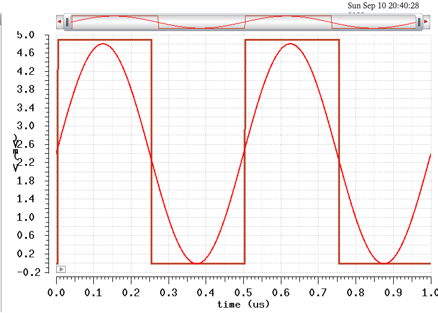
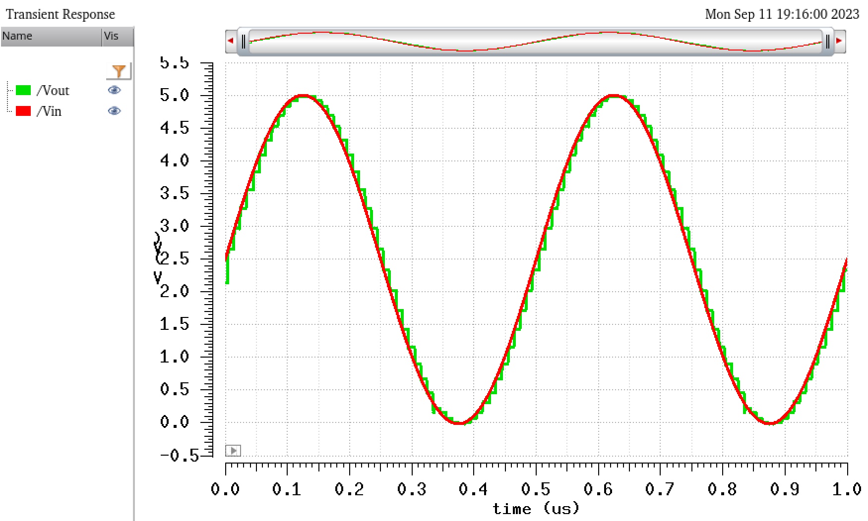
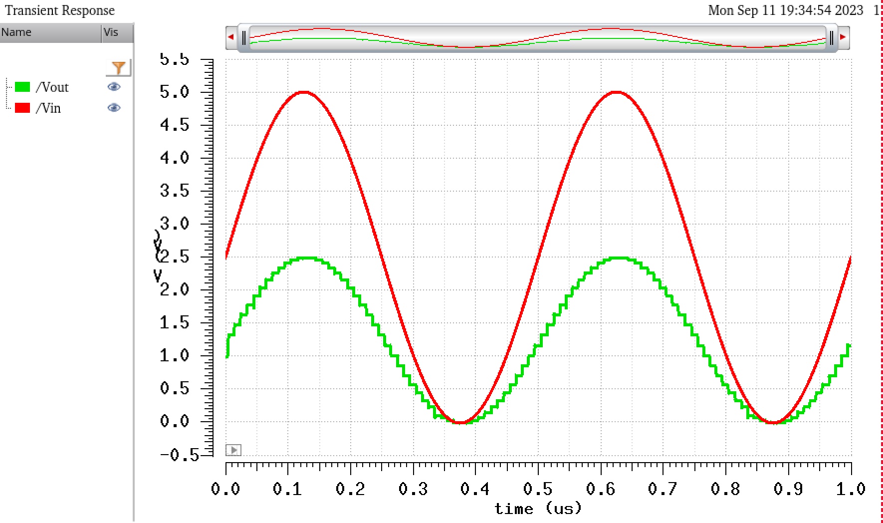
We then Launch ADE L, go to Load state and press the green button to get our netlist and simulation for this ideal ADC_DAC file Dr.Baker provided for us. The following graph should appear.
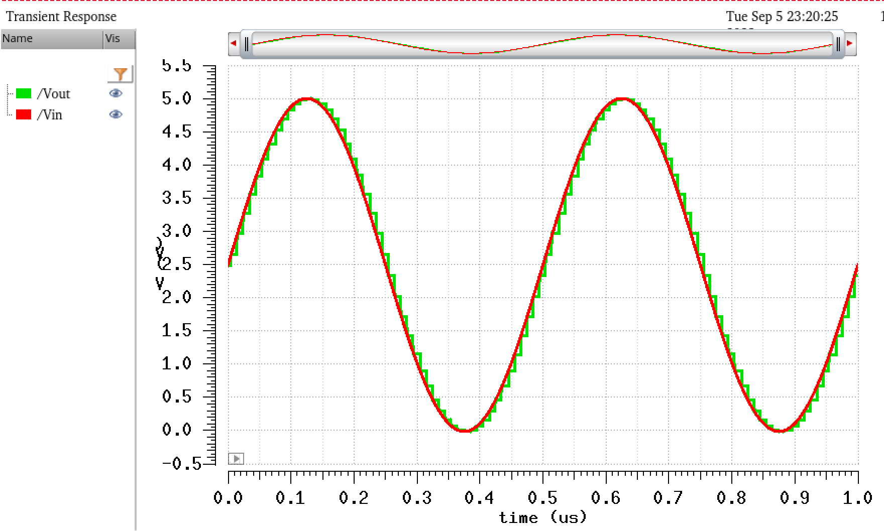
Here I have changed the lines to be solid and thick. This is done by right clicking the value on the left most list then going down to width and style. Color can also be changed like this.
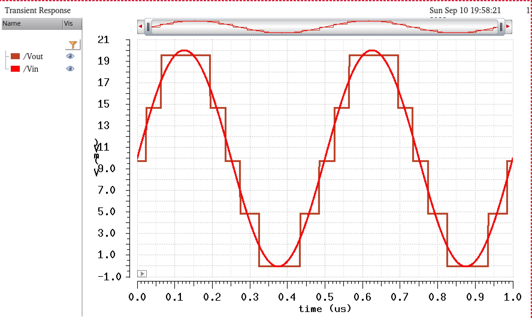
Now we are asked to modify the waveform so we are able to see the output steps better.The best of achieving this is by changing the input voltage Vin to a different number. In the image below 10mV with an offset of 10mV was used as this provides a nice view of the step output wave for Vout.
One final thing we are able to do is to find the LSB or Least Significant Bit of this setup. Which can be calculated by the equation: LSB = VDD/2^N. Here we get 5V/ 2^10 = 4.883mV. And if we set the voltage to that value we can see the minimum voltage change possible for this B[9:0] digital code waveform.
Prelab Questions:
How is Vin related to B[9:0] and Vout?
The relation between the two is that Vin is taken and converted to it's B[9:0] form which is a 10-bit binary representation. B9 being MSB (Most significant bit) and B0 being LSB (Least significant bit). B[9:0] is the output of the ADC, that then becomes the input of the DAC. It intakes the 10-bit number and converts it into an analog waveform. Meaning, Vout is the analog representation of what we inputted for Vin at the start.Lab Work:
To start off we must create our own DAC using an N-well Resistor with a value of 10k.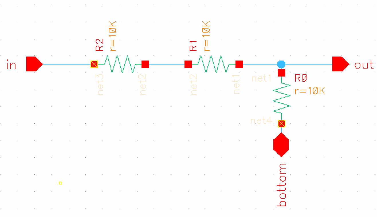
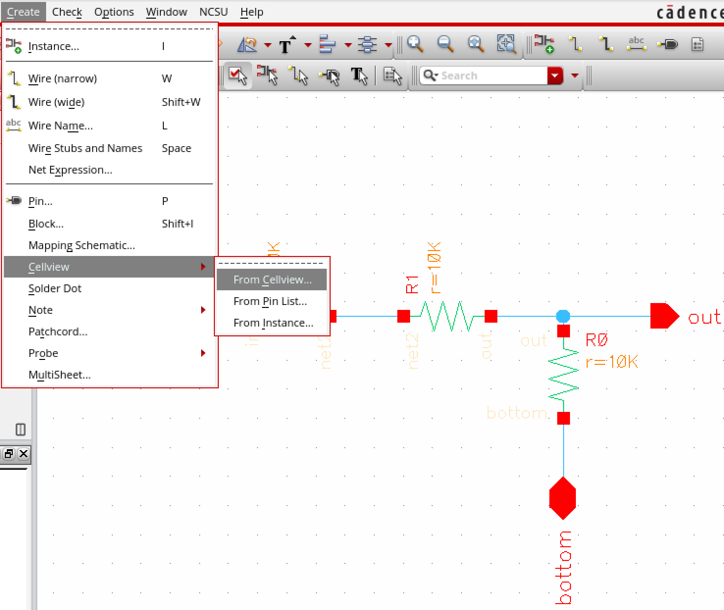
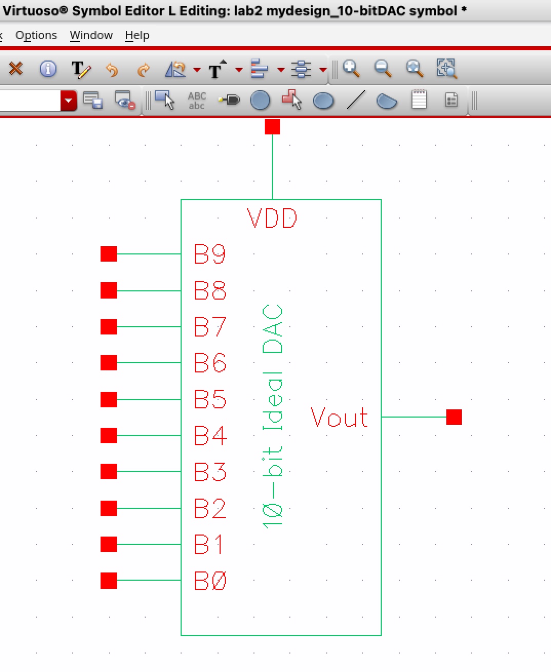
From here we need to got to Create -> Cellview -> From Cellview in order to make the following symbol. This is a 1-bit DAC.
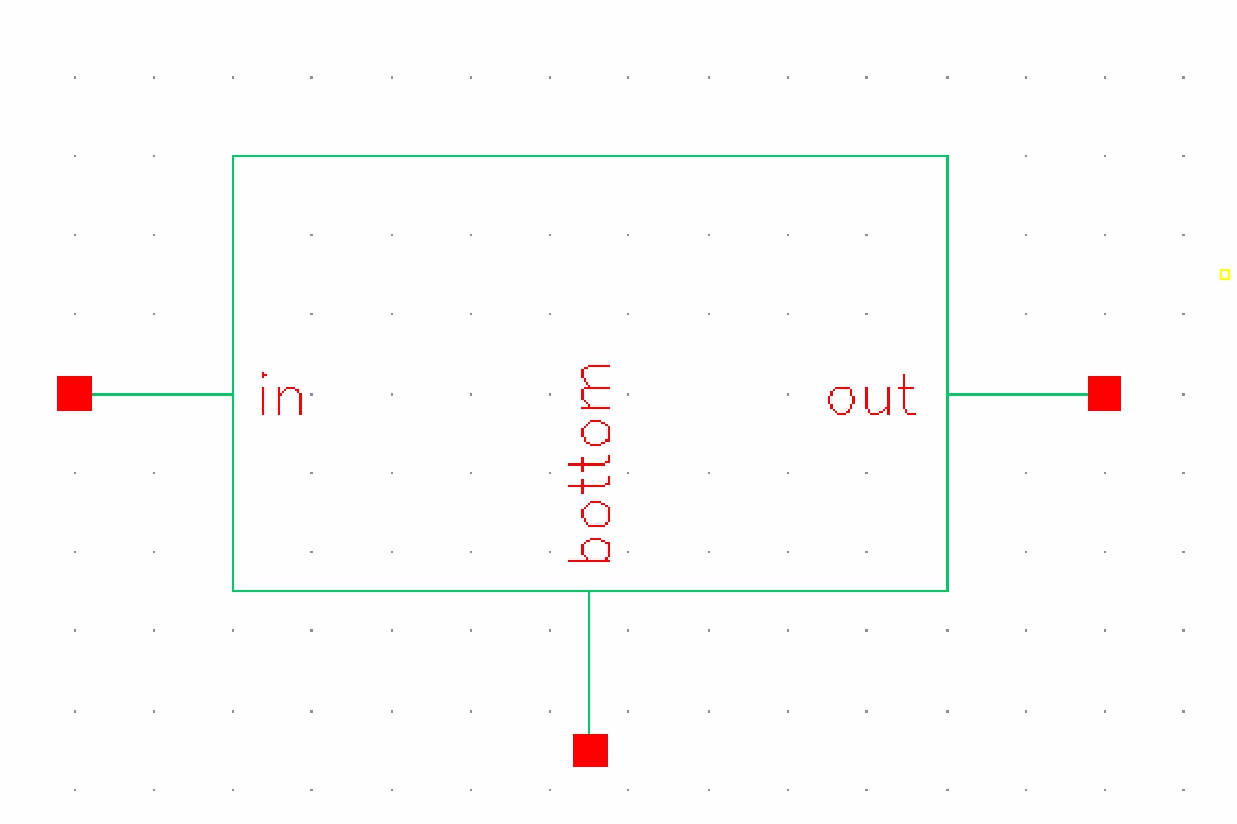
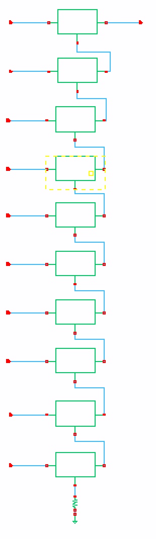
We now must make a new schematic by cascading 10 of the 1-bit DAC symbols made in the previous step and then adding a 10k resistance at the very end. We also add pins going from B0 to B9 and a Vout pin. This is the basis of our 10-bit DAC. In the same way as the last step we make a symbol, however we were advised to simply copy over the Ideal DAC symbol provided in the lab2.zip. The only difference is we need to delete VDD, Vrefp and Vrefm as we will not use them in our design.
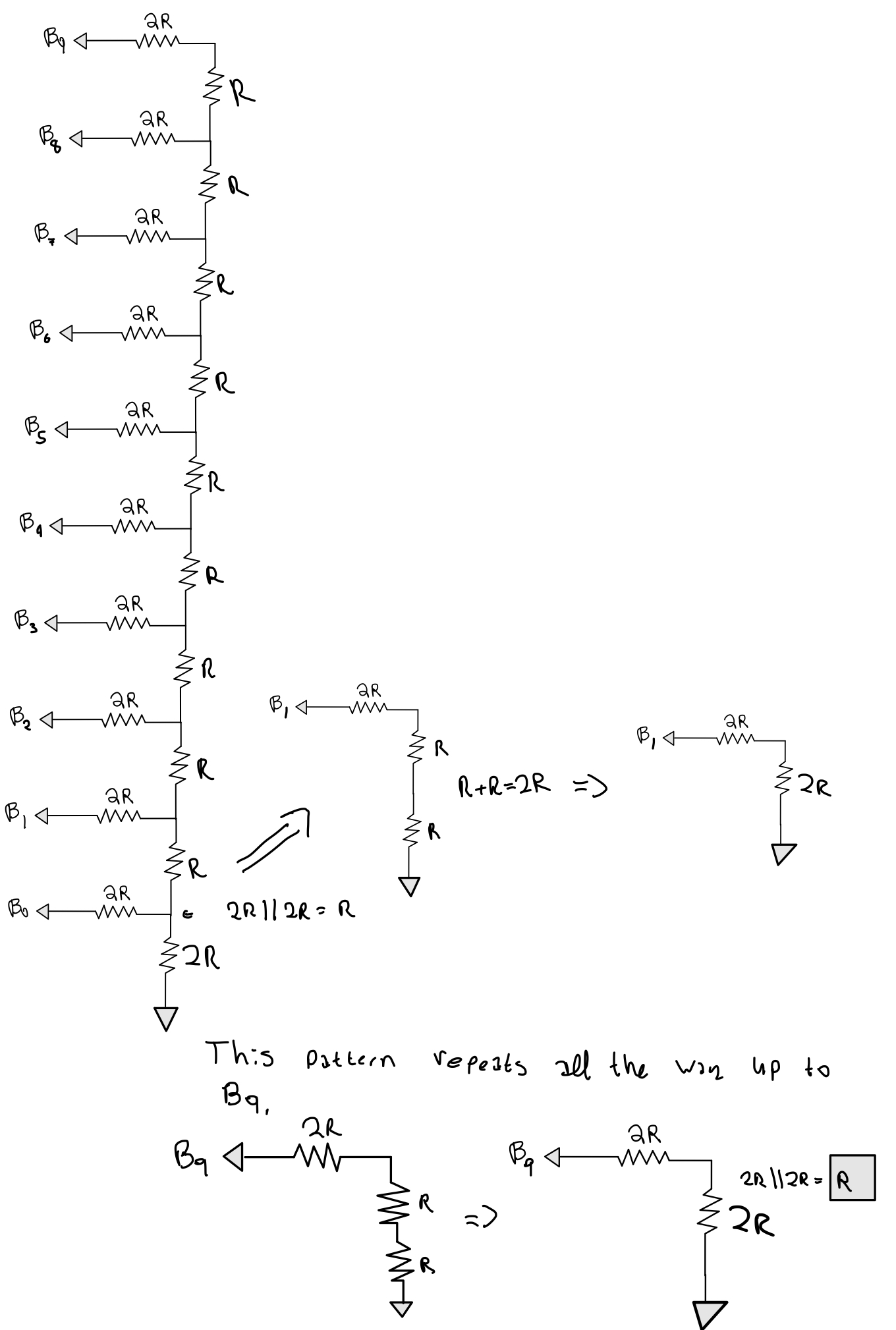
Finding 10-bit DAC resistance:
To start this process we need to need to realize several circuit rules we should be familiar with. First we should ground every bit value from B[9:0], notice at the bottom of the circuit we now have 2 resistors of 2R value in parallel. The value can be simplified to just a value of R. Which then becomes in series with another R resistor making 2R, which leaves us in a similar situation. Working up from there we can see this pattern repeats all the way up to B9 input leaving us with a final resistance value of R.
Delay Due to Driving Load:
By adding a capacitor value of 10pF to this circuit as a load we introduce a time delay which is expected because of the 10K resistor in the DAC we have essentially created an RC circuit.With R = 10k and C = 10pF. By an RC circuit definition we can calculate this time delay by the formula td = 0.7RC.
td = 0.7RC = 0.7 * 10k * 10pF = 70ns
By simulations we can confirm this is true.
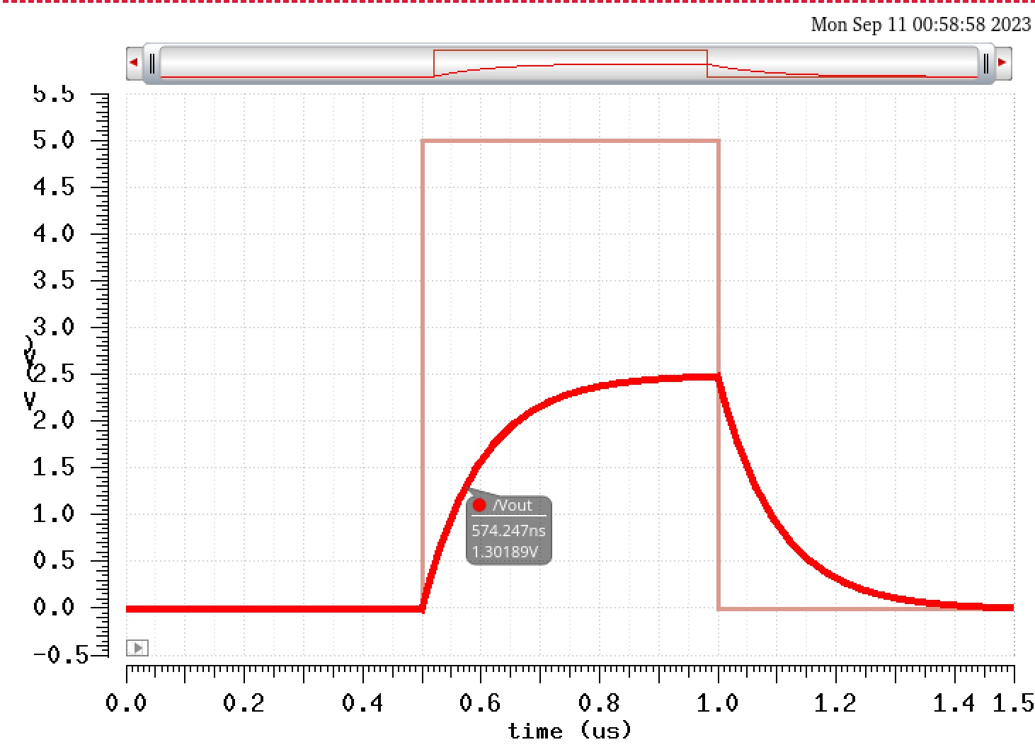
When the voltage reaches 1.25 which is half of the peak we get around 570ns, subtracting the delay time we input into the pulse source which is 500ns, we get: 570ns - 500ns = 70ns.
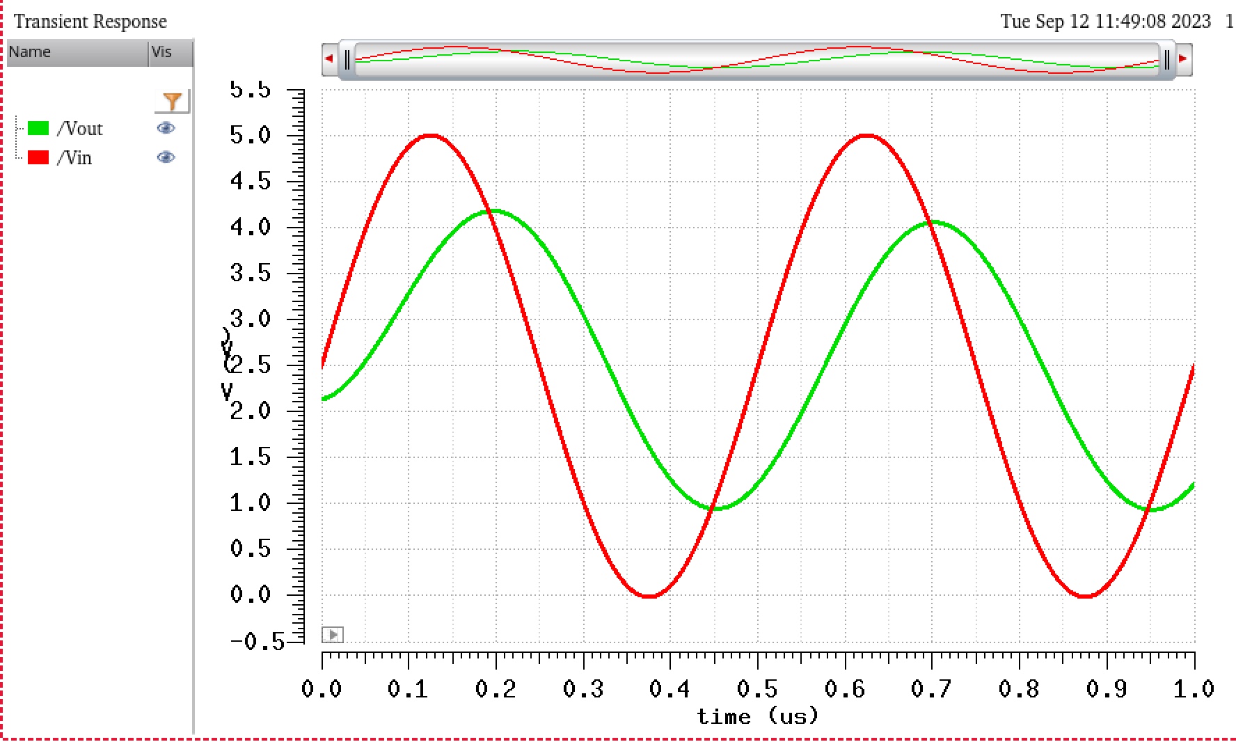
ADC to DAC simulation, No Load:
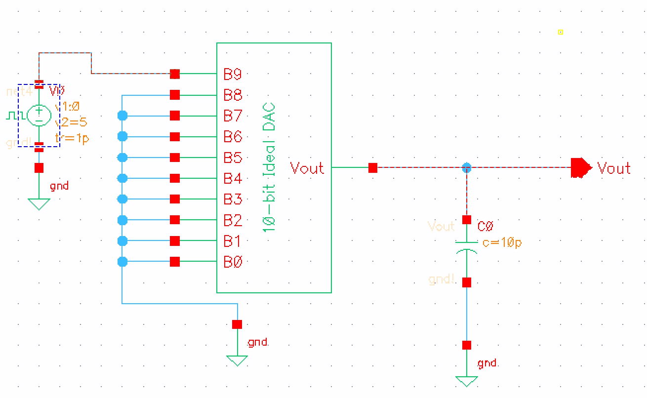
Now we are ready to add our DAC to the ideal ADC provided for us to make our own 10-bit ADC_DAC. Note: Before we tried to simulate, we had to lower VDD value from 5V to 4.99V. It is unclear why but it would not sim at 5V.
Simulating the circuit above will yield the following result. Which we should recognize as being the similar to the simualtion we got for the ideal 10-bit ADC_DAC.
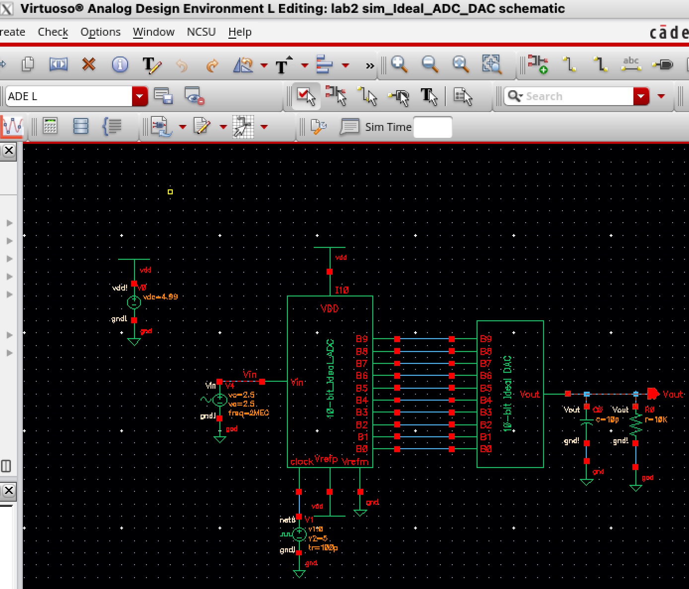
ADC to DAC simulation, 10k Load:
Now we want to add a 10k resistor as a load to our design to see how it will affect the Vout analog waveform.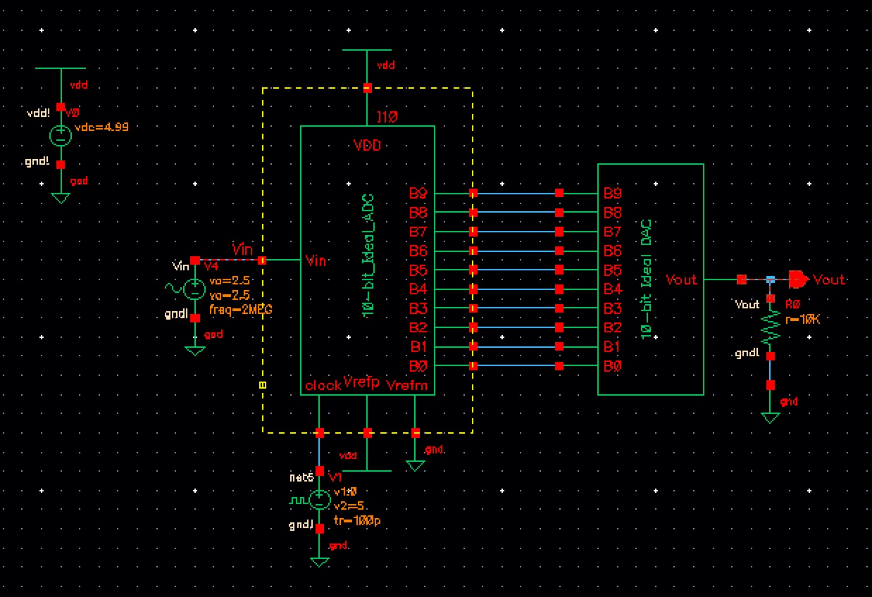
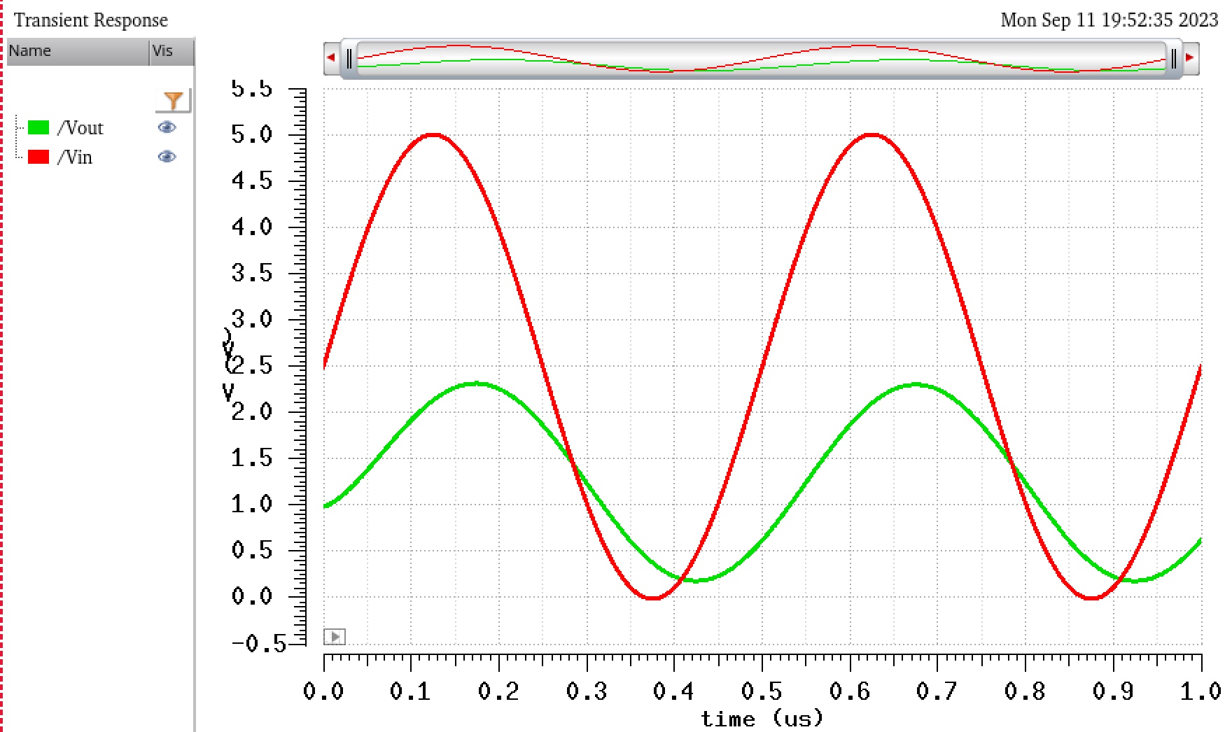
ADC to DAC simulation, 10pF Load:
As we calculated earlier there will be a time delay if we add a capacitor since we effectively turn this into an RC circuit.
The capacitor will make a time delay of 0.07us but it will also cause a DC offest of about 2.5V. It also makes the analog wave a continuous wave for Vout. This makes sense as capacitors resist changes in voltage.
ADC to DAC simulation, 10k & 10pF Load:
By adding both a resistor and a capacitor we get an amalgamation of the two results we see from the eariler examples. A delay and a continuous wave, that appears to be half of Vin's magnitude.