Lab Project - ECE 421L
Authored
by Martin Mercado mercam13@unlv.nevada.edu,
11/22/2023
Lab Project:
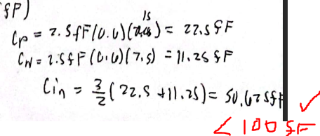
Design a non-inverting buffer circuit that presents less than 100 fF input capacitance to
on-chip logic and that can drive up to a 1 pF load with output voltages greater than 7V (an output logic 0 is near ground
and an output logic 1 is greater than 7V). Assume VDD is between 4.5V and 5.5V, a valid input logic 0 is 1V or less, a valid
input logic 1 is 3V or more. Show that your design works with varying load capacitance from 0 to 1 pF. Assume the slowest
transition time allowed is 4 ns.
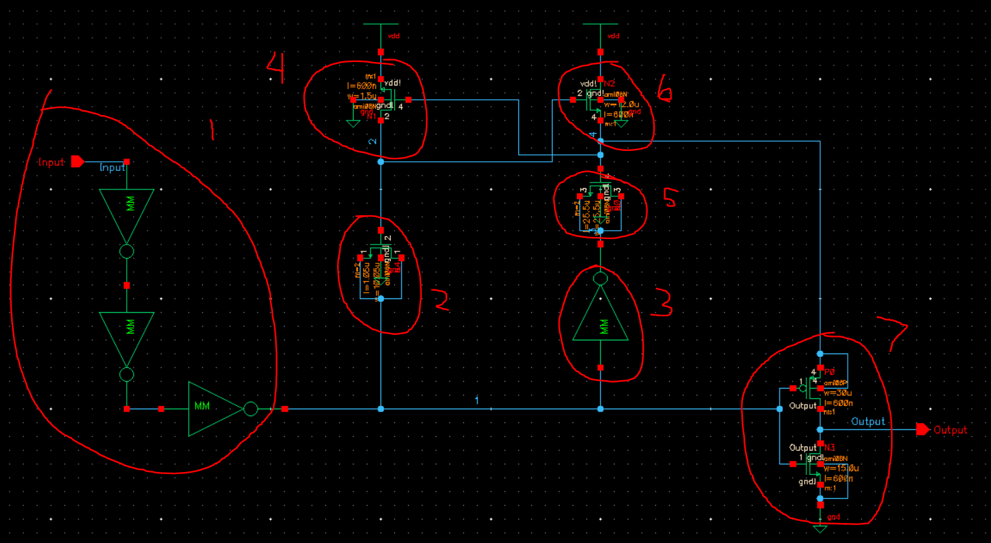
Circuit:
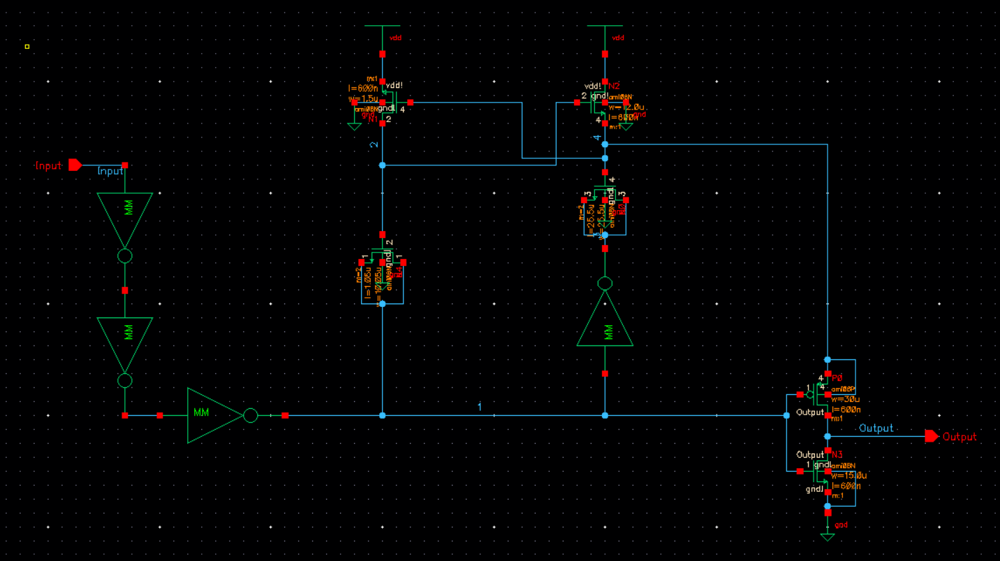
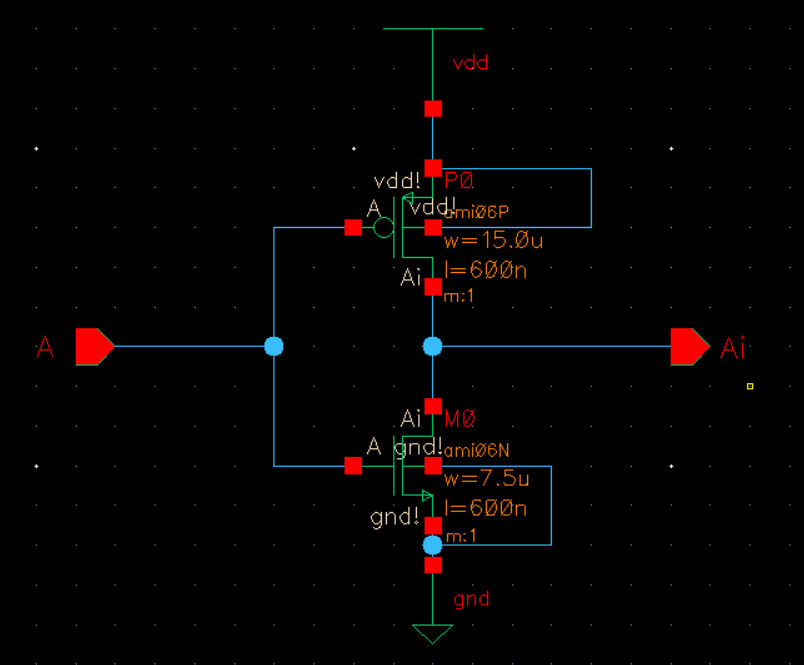
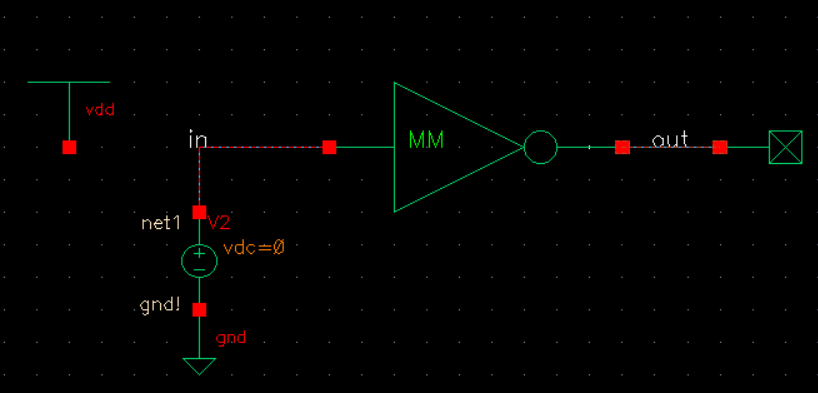
Inverter:
First,
I will be calculating the size of an inverter that would
satisfy an input capacitance of less than 100fF and a transition
time less than 4ns.
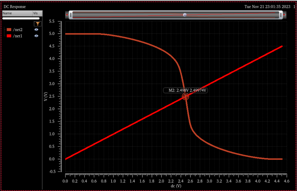
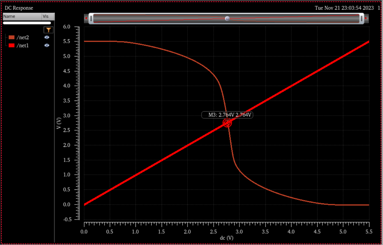
When calculating the size of the inverter, I
would have to keep in mind that the ideal switching point is VDD/2 for
best performance.
In this project, VDD will be from 4.5V to 5.5V so ideally the switching point, Vsp, would be from 2.25V to 2.75V.
In
order to achieve a switching point of 2.25V to 2.75V, I would need to
have the width of the PMOS twice as big as the NMOS (Wn=2Wp).
This also makes both the NMOS and PMOS of the inverter have equal resistances.
NMOS and PMOS Resistance: Total Input Capcitance:
Verify
that the switching point is VDD/2:
4.5V:
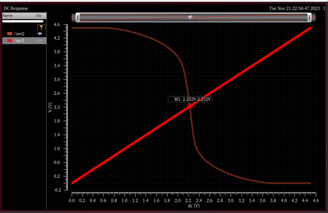
5V:
5.5V:
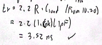
Next, I will calculate the transition time.
The project requirment is less than 4ns.
Transition Time:
Mosfet Capacitor that shares a charge with the load capacitor (Max: 1pF):
I will be using the the equation below to calculate the capacitance of the Mosfet.
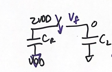
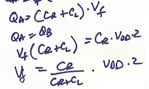
After trying different values for the capacitance I decided to go with 6.25pF.
Vf<(C1/(C1+C2))(2Vdd)
7V<(6.25pF/(6.25pF+1pF))(4.5(2))
7V<7.714V check
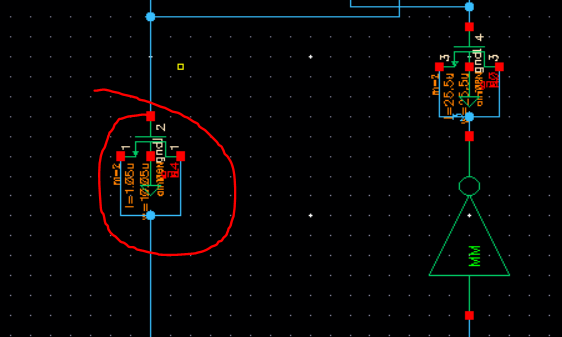
C1=2.5WL=6250fF
WL=2500
50x50=2500
The length will be L and N would 50.1 to be on grid.
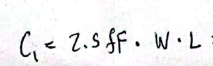
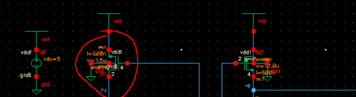
Next, I will calculate the size of the Mosfet N4.
This Mosfet capacitor will be used to charge the node 2 and turn on NMOS N2.
Node 2, where the Mosfet capacitor is connected to, does not supply to the output voltage of the circuit.
Making it small will minimize layout area.
For this reason, I chose a capacitance of 100fF.
Just so the sizing of the Mosfet capacitor will be on the grid, I will change the values to L=2.1 and W=20.1
NMOS N1:
NMOS N1 can also be small because it does not affect the output voltage of the circuit.
Making it small will minimize layout area and power.
NMOS N2:
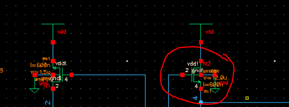
NMOS N2, when turned on, is used to charge node 4 to VDD.
Therefore I chose a bigger NMOS so the resistance is lower and drive a higher current.
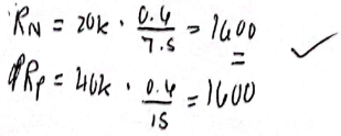
PMOS P0 and NMOS N3:
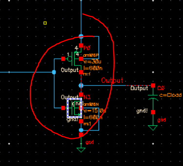
I
chose 30u for the PMOS and 15u for NMOS to make the resistances equal
and have the output as close to 2VDD with as little overshoot voltage.
Rp=40k(.6/30)=800ohms
Rn=20k(.6/15)=800ohms
Input Inverters:
I used 3 Inverters to buff the input.
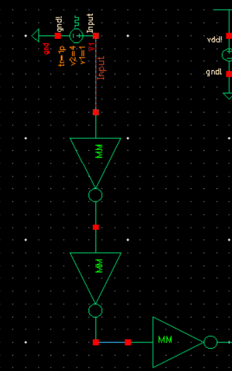
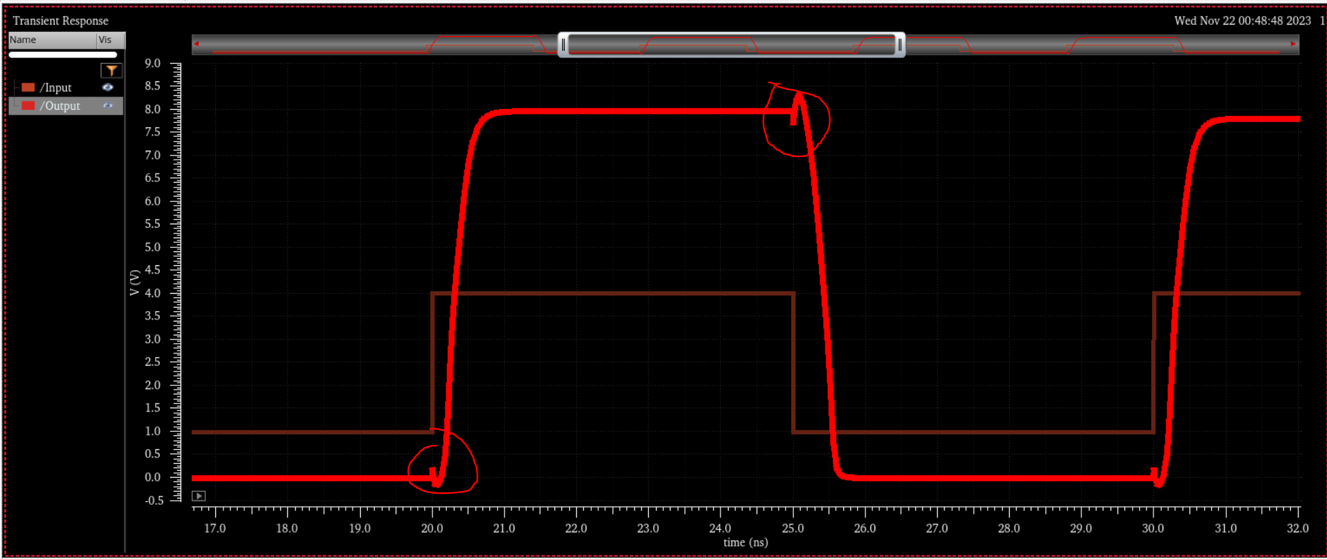
Output with 1 Inverter:
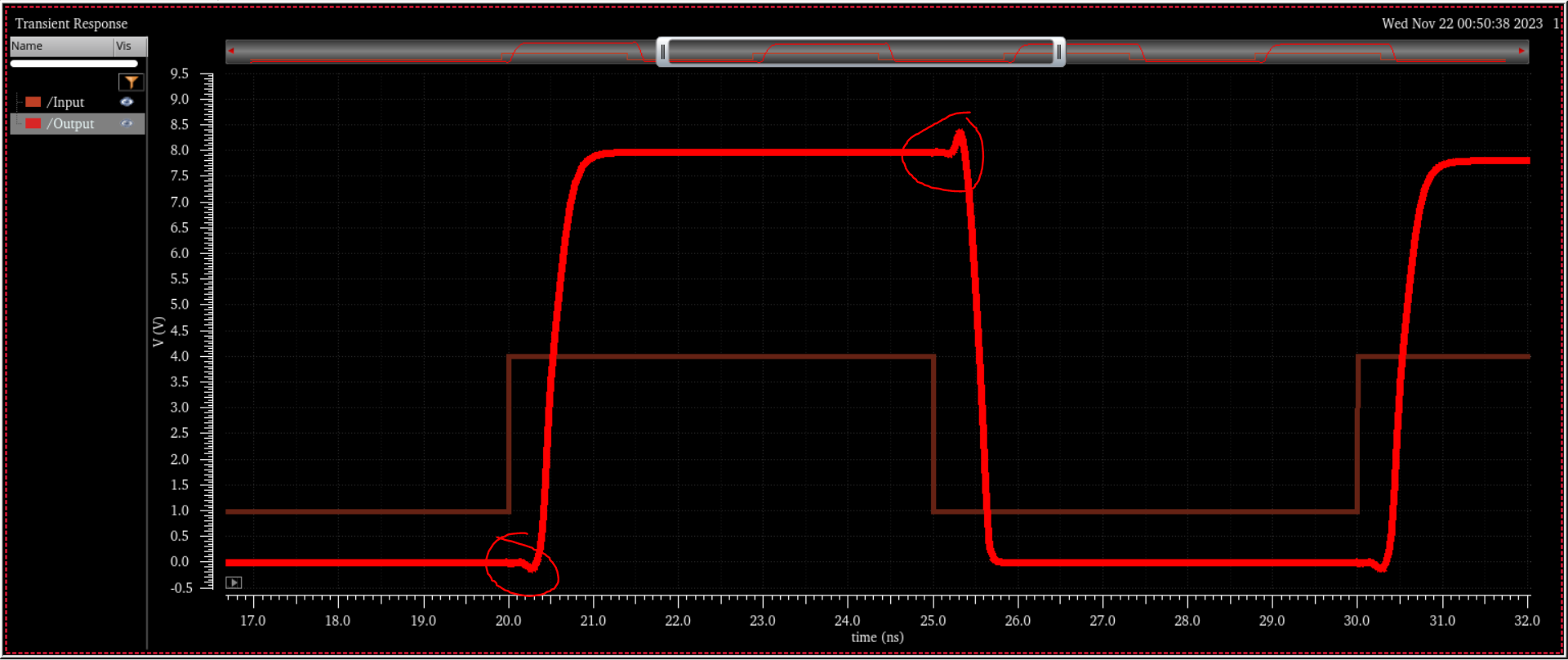
Output with 3 Inverters:
Circuit Function:
Input Logic Low:
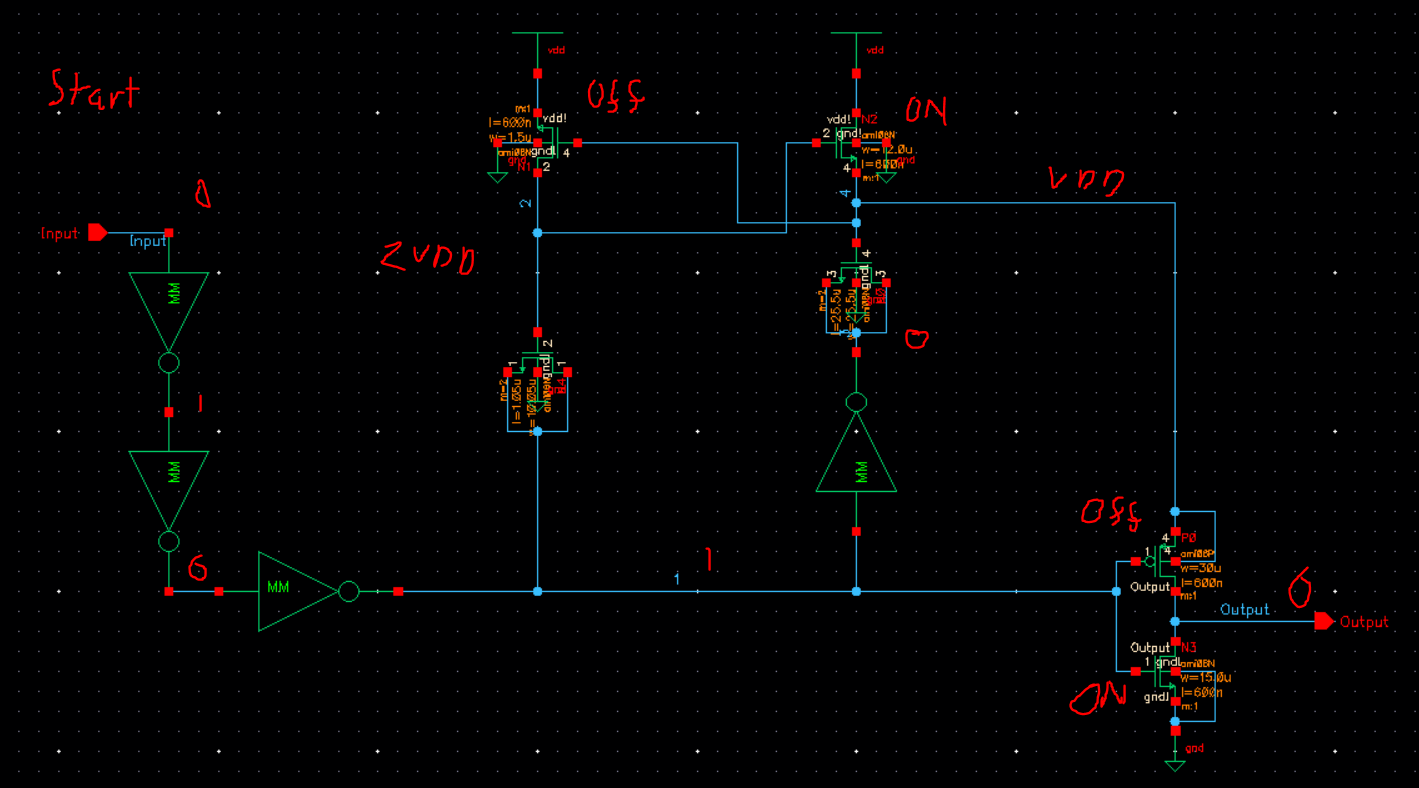
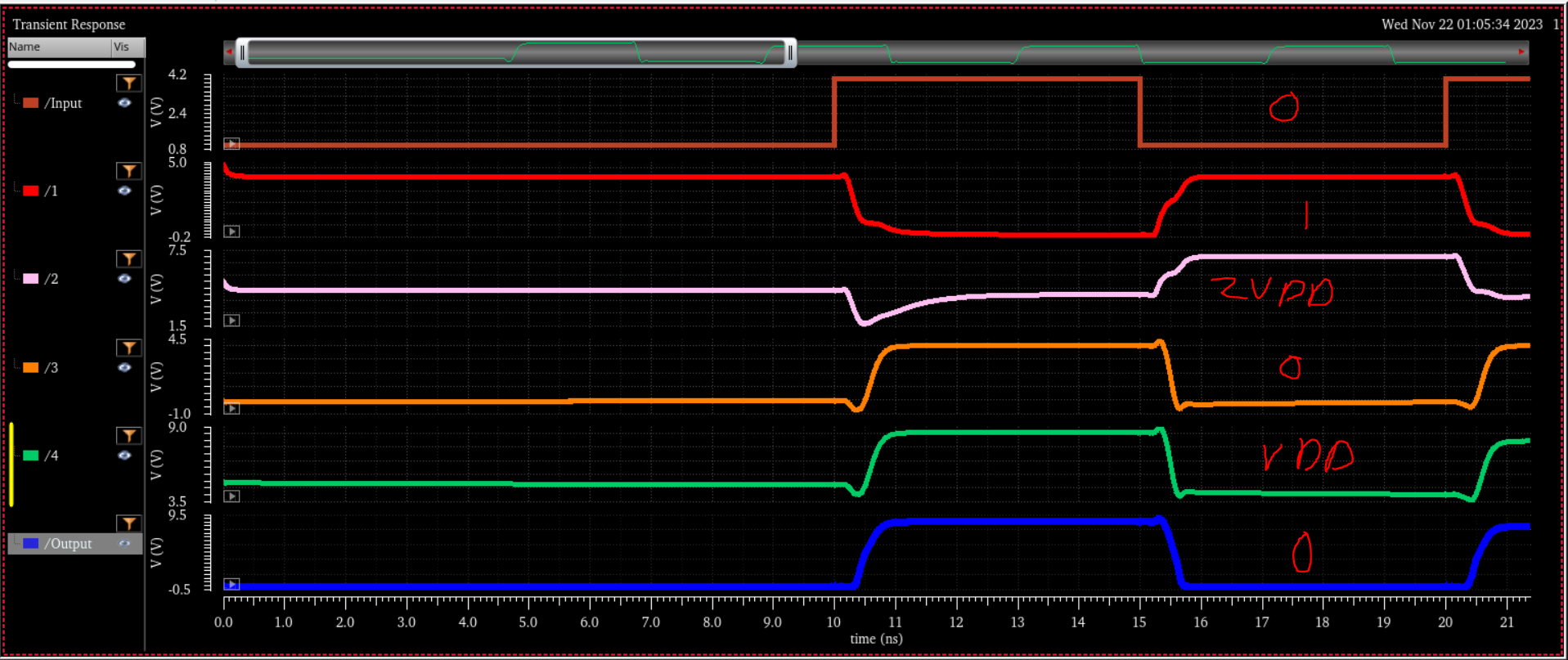
When Input logic is low, Node 1 would be logic high. Node 3, after the inverter, would be logic low.
Node
2 would then be at 2VDD turning on NMOS 2. Node 4 would be VDD, keeping
NMOS 1 off. PMOS 0 would be off and NMOS 3 would be on
The output of the driver would then be logic low 0 (ground).
Input Logic High:
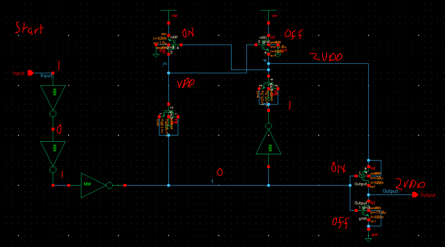
When
Input Logic is High, node 1 would in logic low. Node 3, after the
inverter, would be logic high. Node 4 goes to 2VDD turning on NMOS N1.
Node 2 would be VDD due to node 1 being logic low keeping NMOS N2 off. PMOS P0 would be on and NMOS N3 would off.
The output of the driver would then be 2VDD.
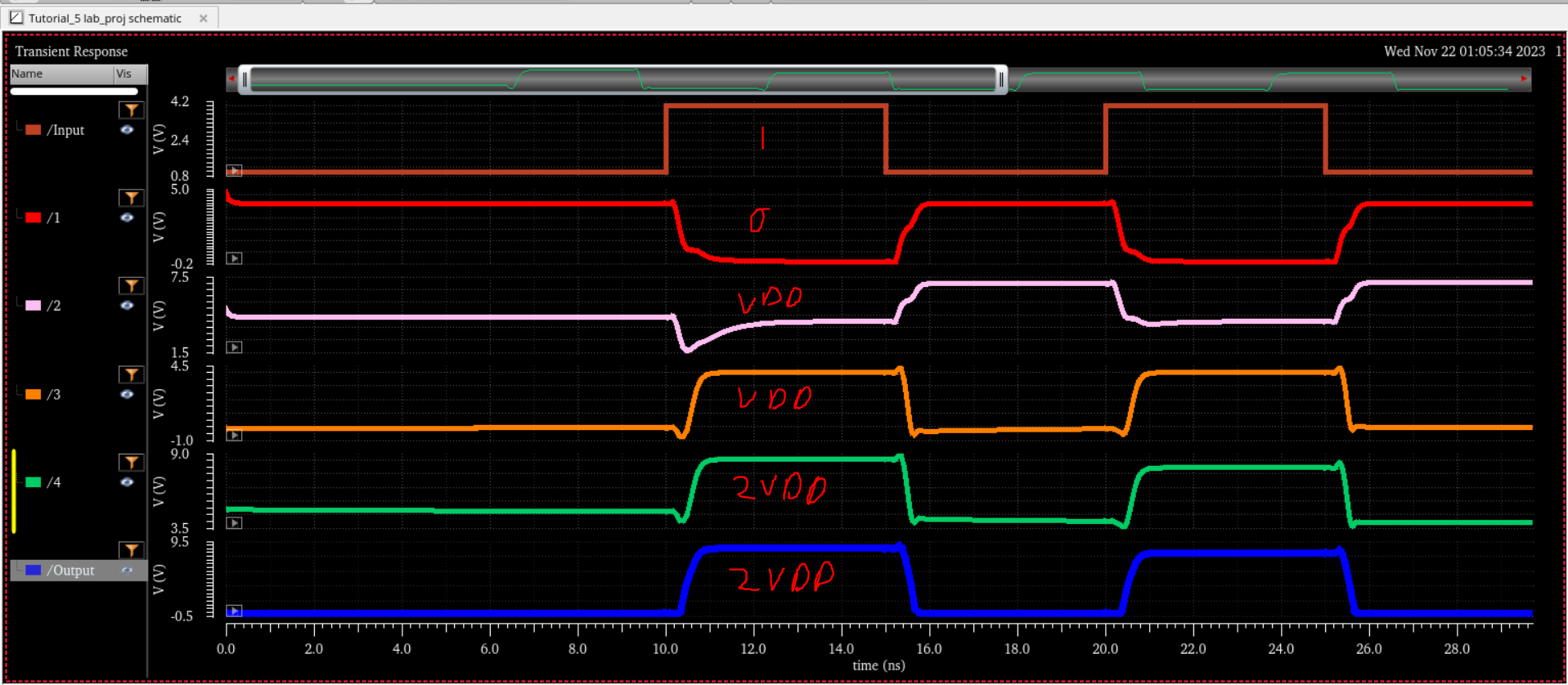
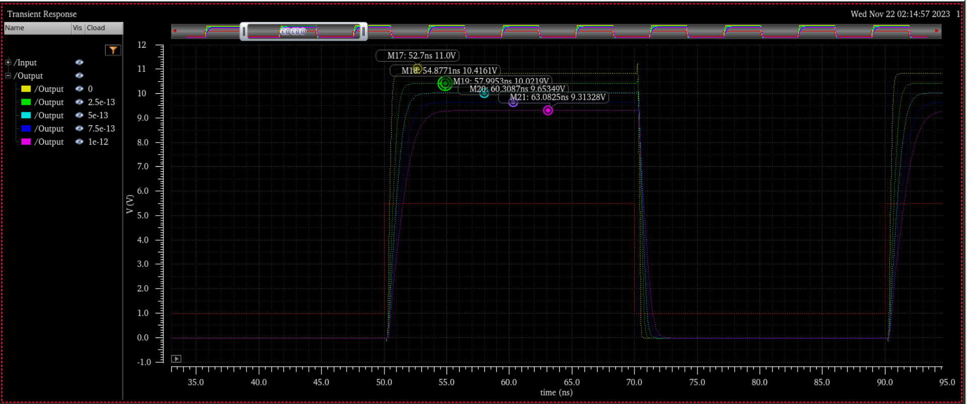
Verify transition time is less than 4ns with 1pF load and 4.5VDD:
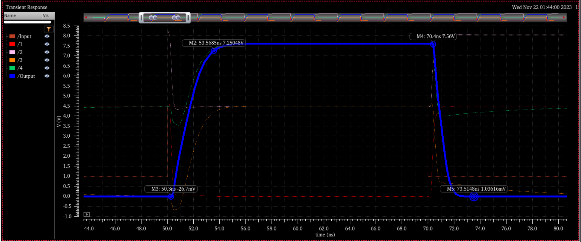
Verify that output voltage is >7 with different loads:
4.5 VDD:
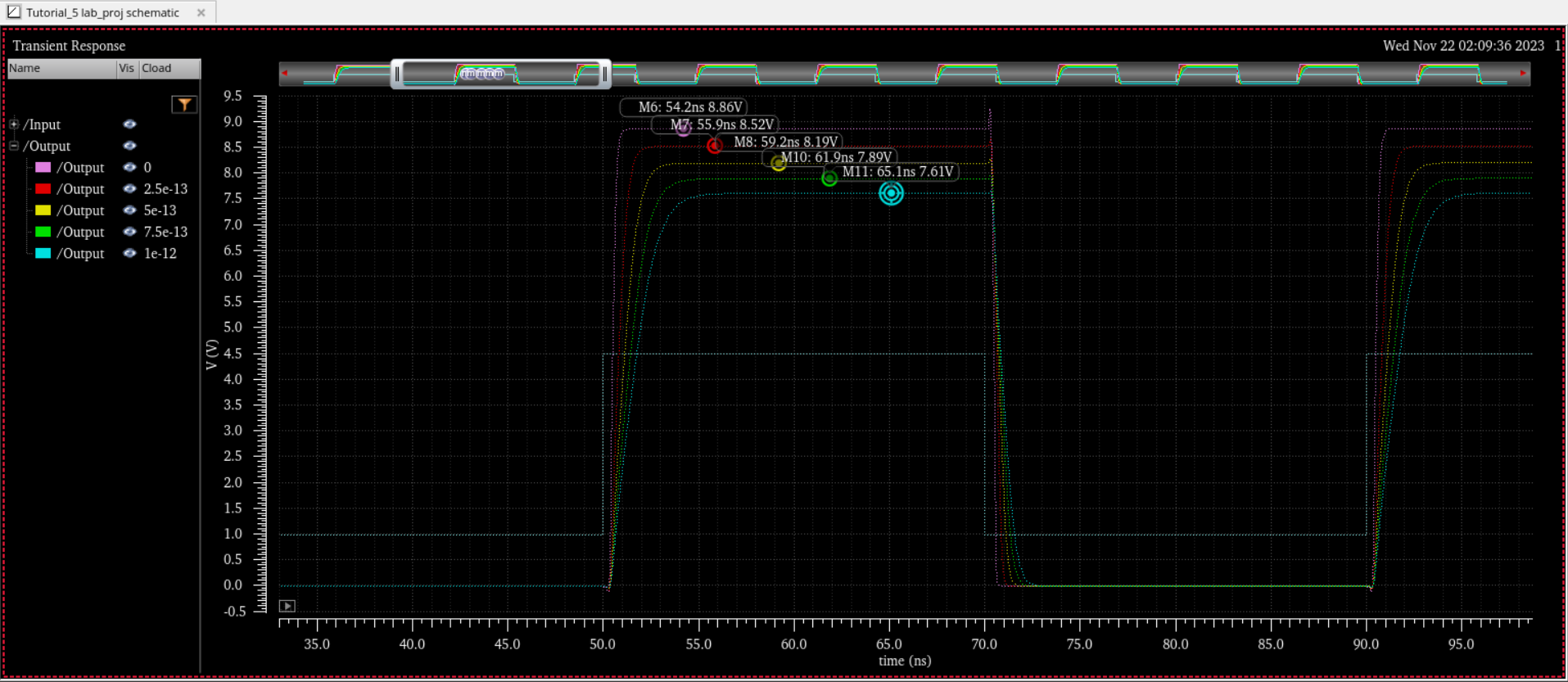
5VDD:
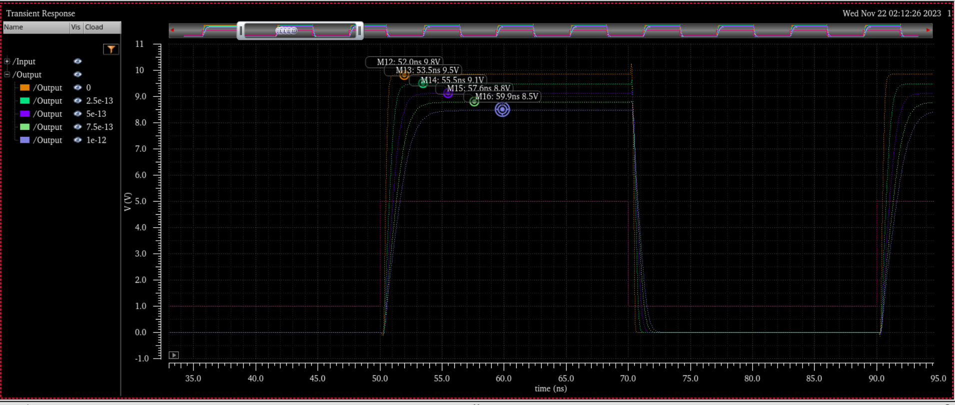
5.5VDD:
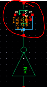
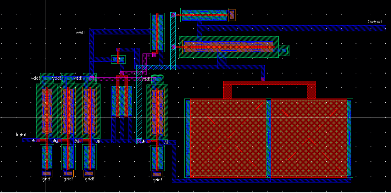
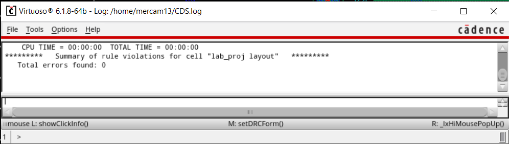
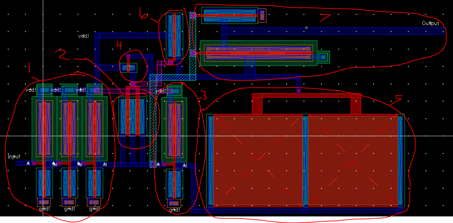
Layout:
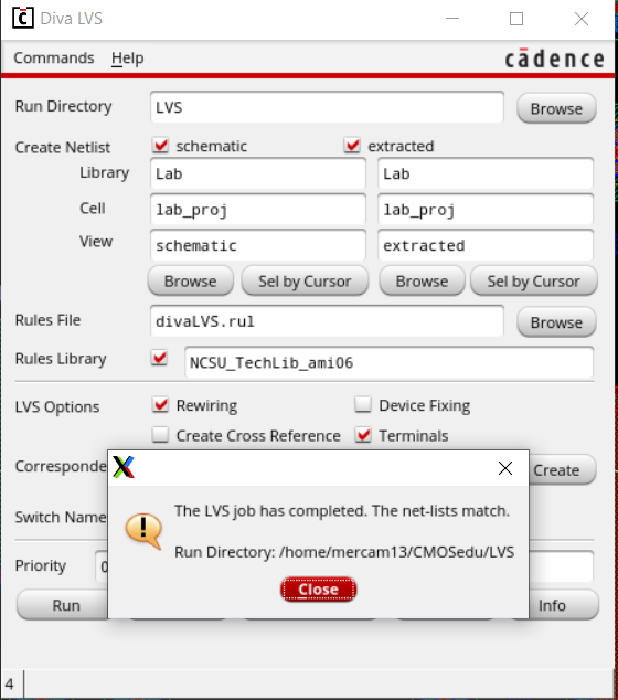
Lab Project Files
Return to EE421 Labs