Lab 7 - ECE 421L
Authored
by Martin Mercado mercam13@unlv.nevada.edu,
11/7/2023
Using buses and arrays in the design of word inverters, muxes, and high-speed adders
Pre-Lab
- Back-up all of your work from the lab and the course.
- Go through Tutorial 5
- Read through the entire lab before starting it.
Tutorial 5:
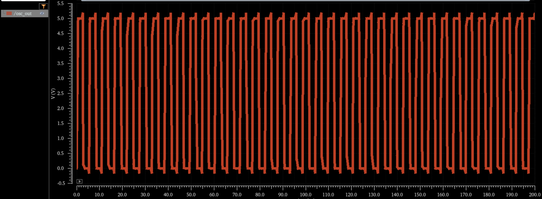
In this tutorial, I will design, layout, and simulate the operation of a ring oscillator.
Schematic:

Simulation after setting initial condition to 0:
Modified Schematic:
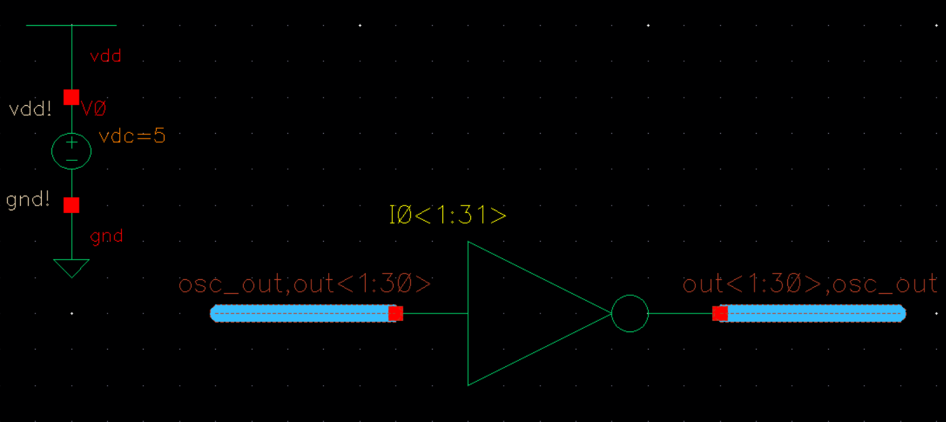
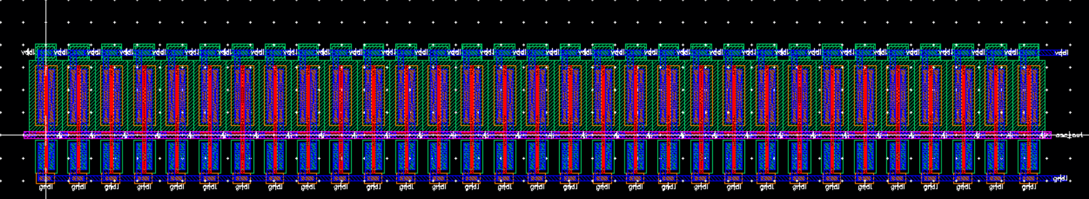
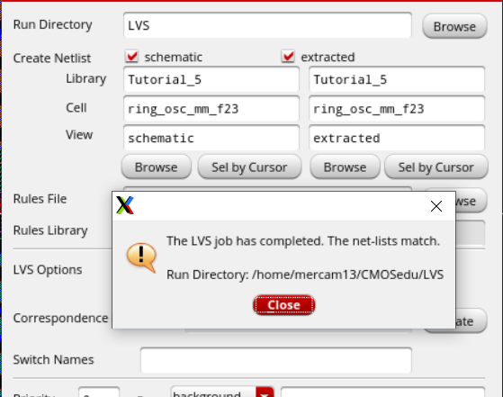
Layout with DRC and LVS:

Now I will create a symbol for the Ring Oscillator.
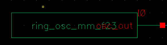
Symbol:
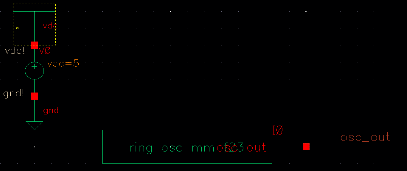
Next I will simulate the Ring Oscillator using the symbol.
Schematic:
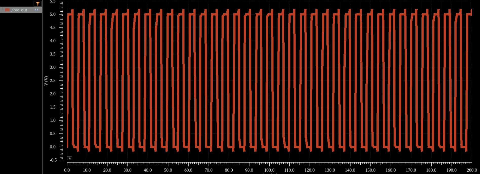
Simulation:
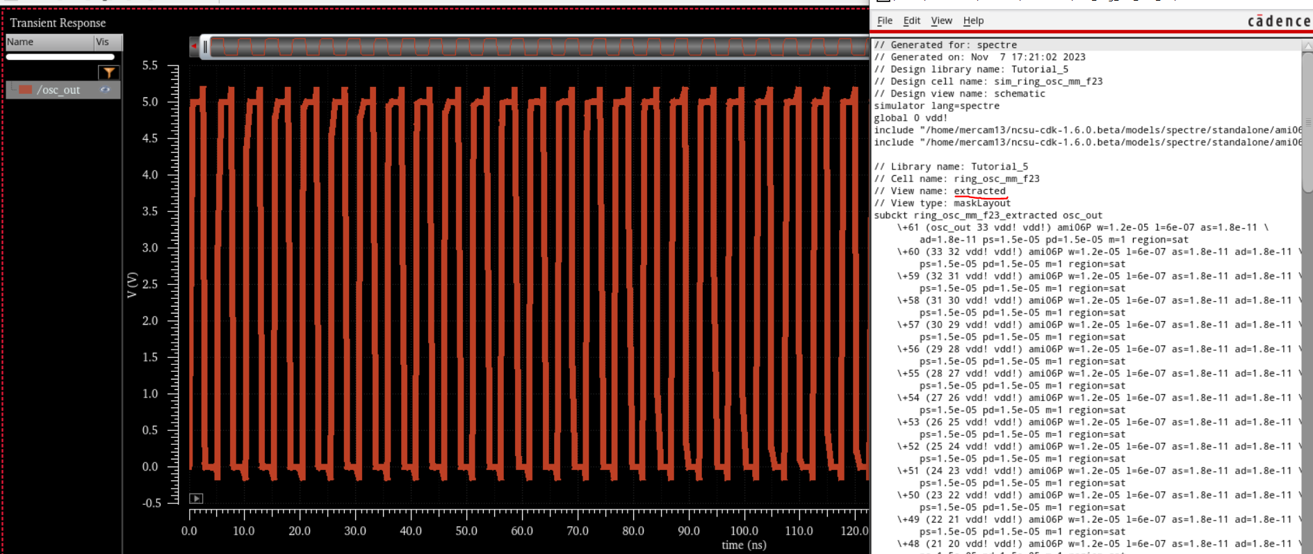
Extracted Simulation:
_________________________________________________________________________________________________________________________
Lab:
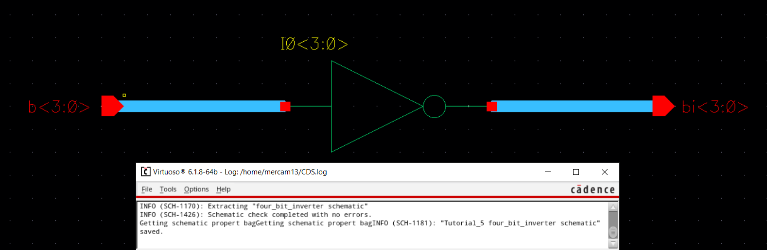
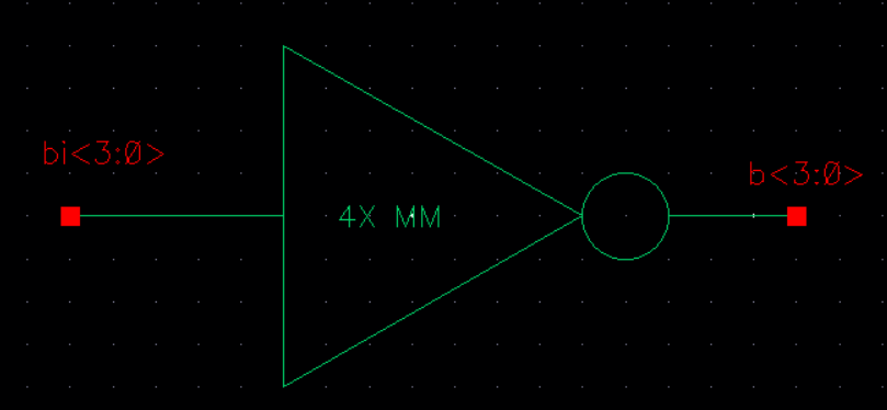
First, I will be designing a four bit inverter using arrays:
Schematic:
Symbol:
Next, I will simulate the operation of the four bit inverter I designed.
Schematic:
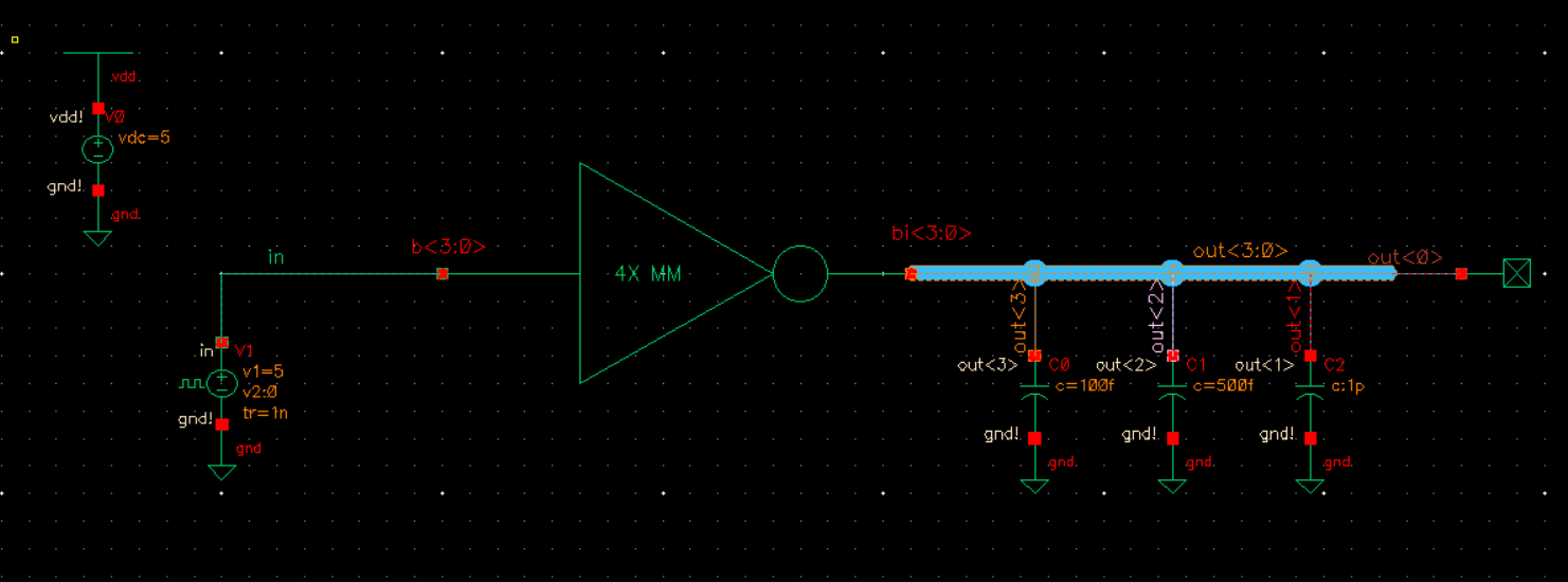
Simulation:
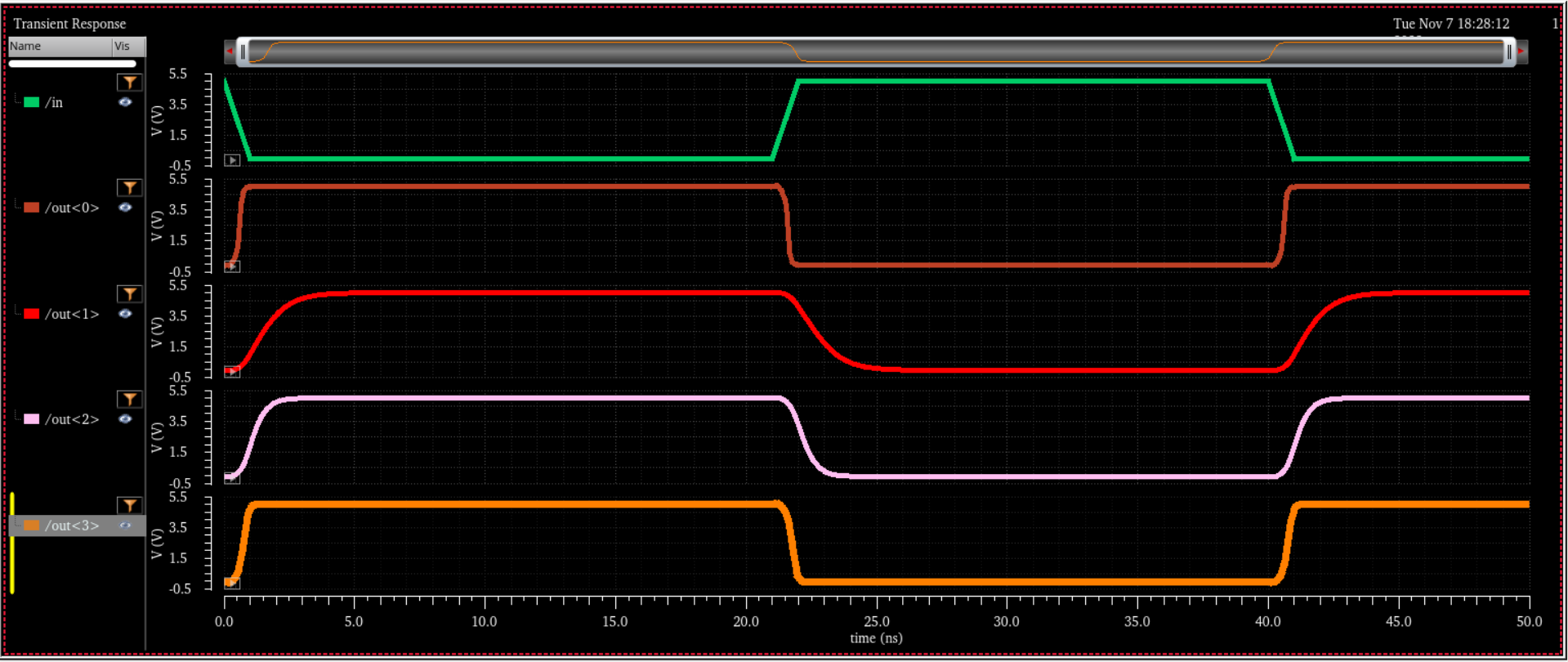
Based
on the simulation results, as the capacitive load gets larger, it takes
longer for the output of the inverter to charge to 5 V.
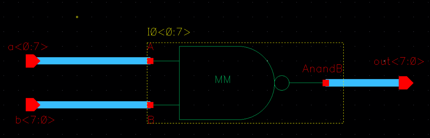
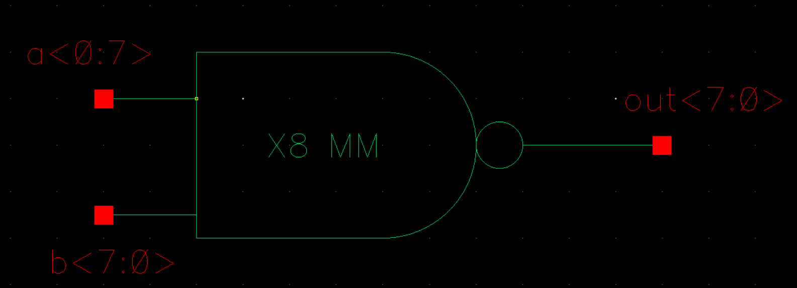
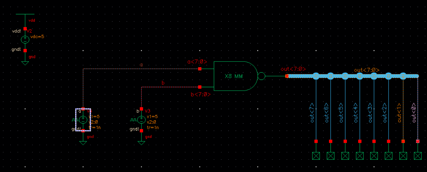
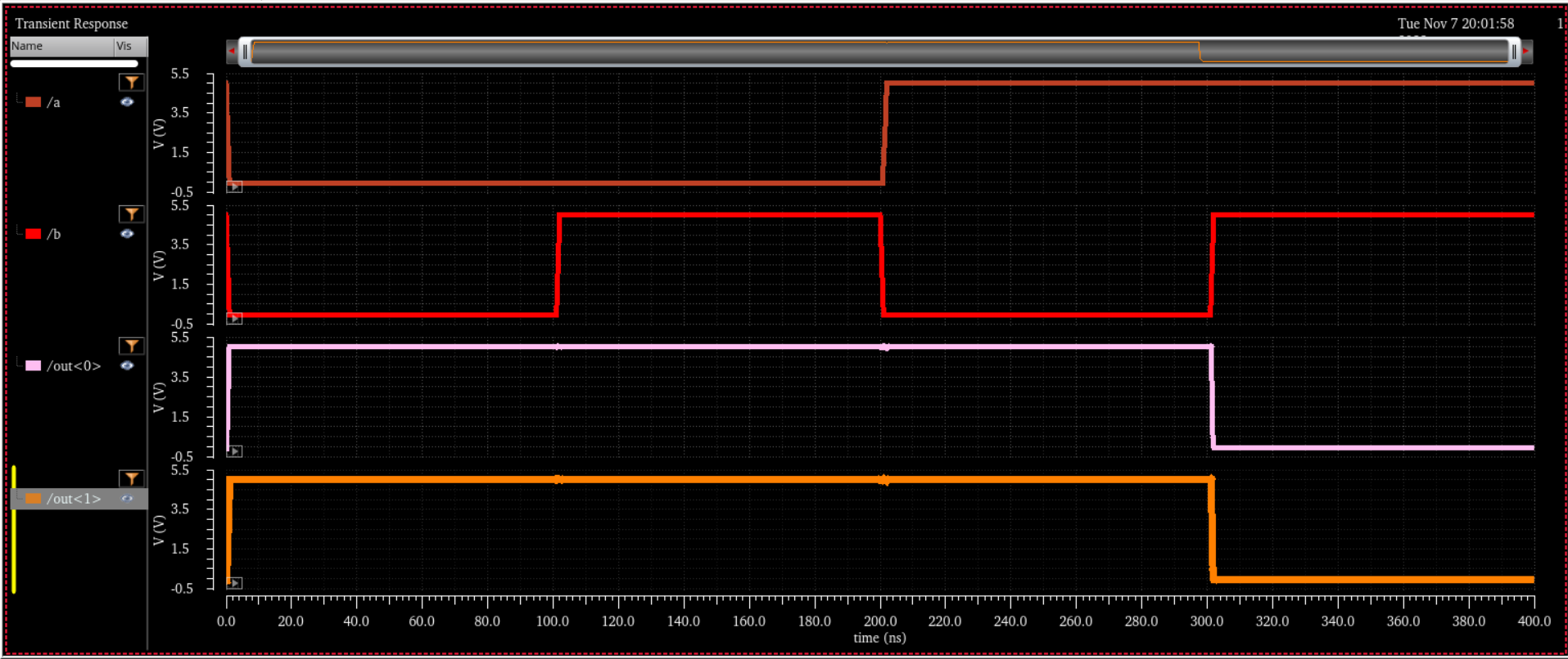
Now I will design an 8-bit NAND gate.
8-bit NAND gate:
Schematic:
Symbol:
Simulation Schematic:
Plot:
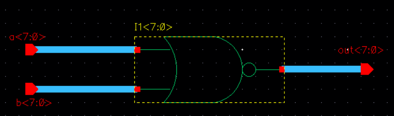
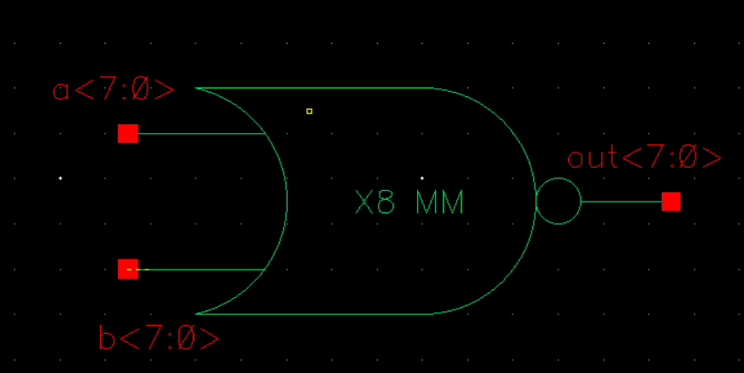
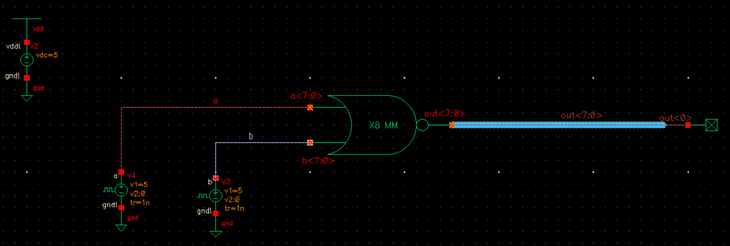
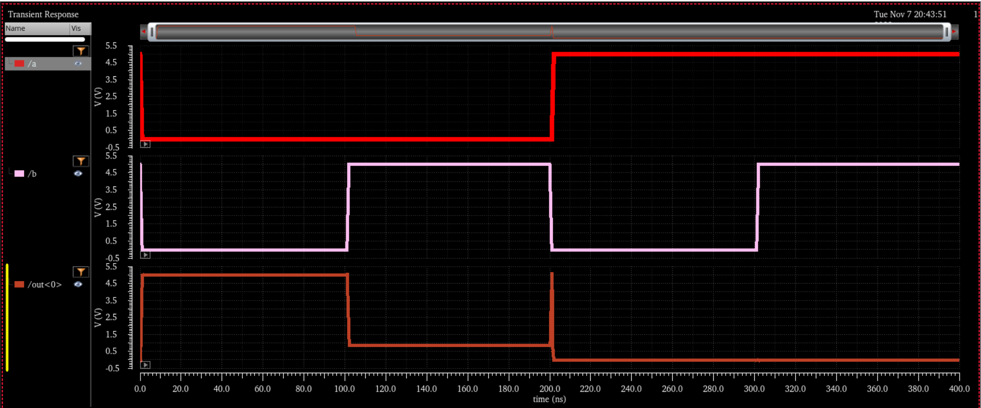
8-bit NOR Gate
Schematic:
Symbol:
Simulation:
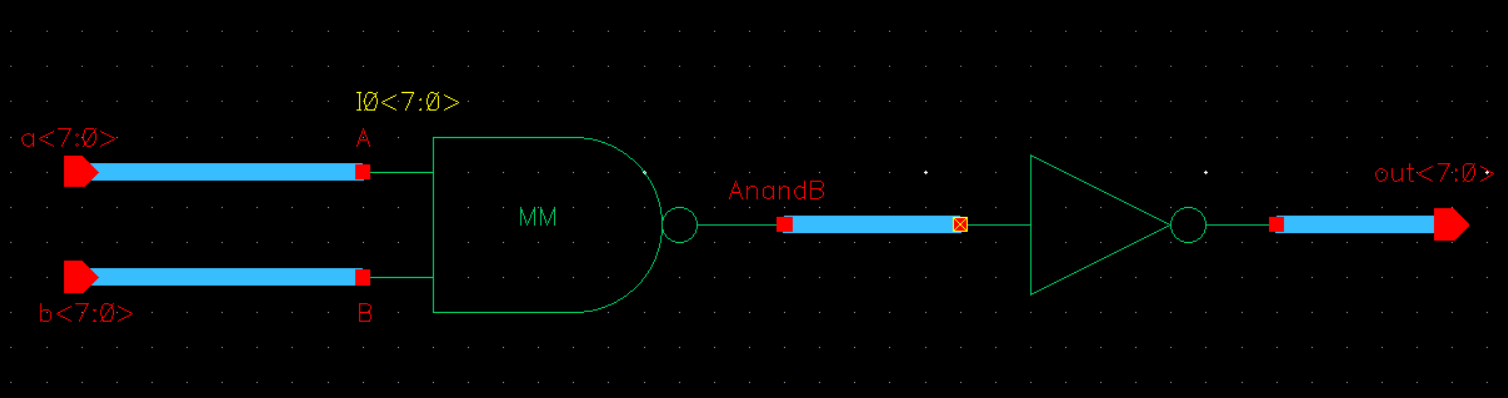
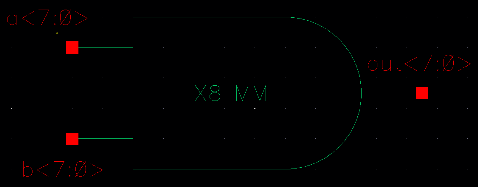
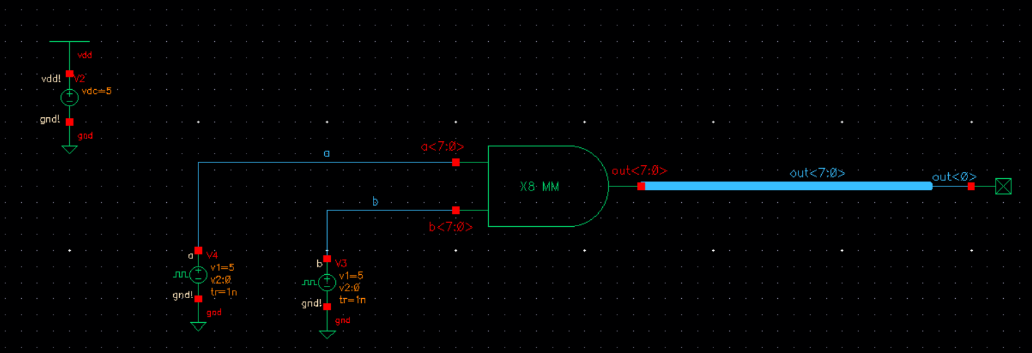
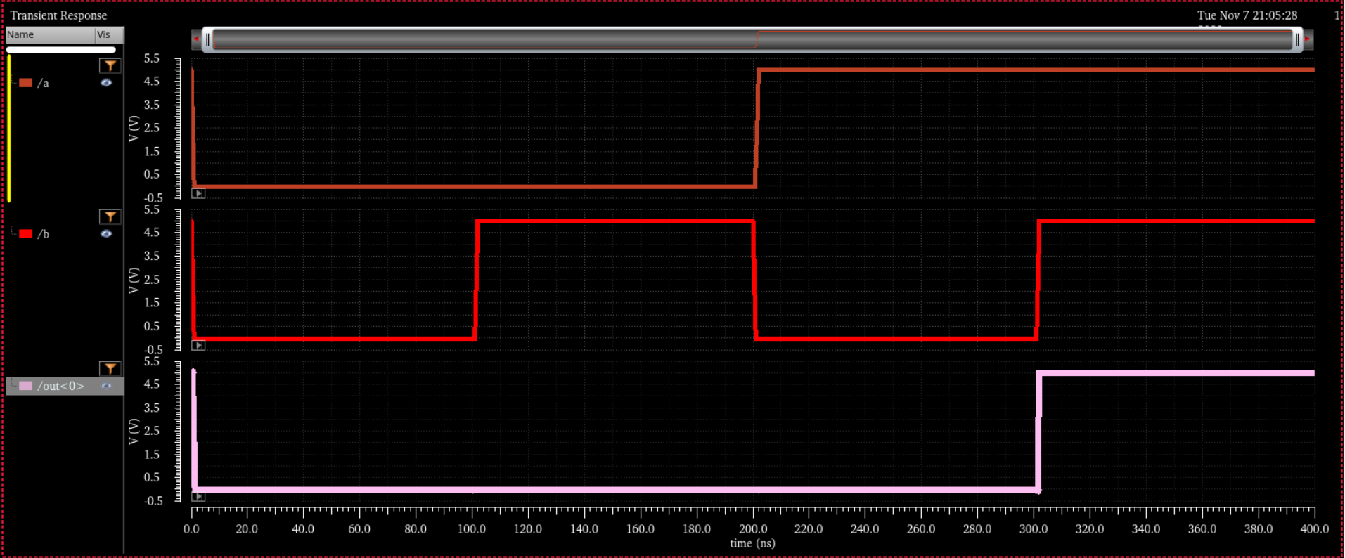
8-bit AND Gate:
Instead of creating a AND Gate from scratch, I added an inverter to the NAND Gate's output to make the AND Gate.
Schematic:
Symbol:
Simulation:
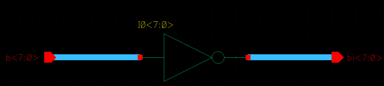
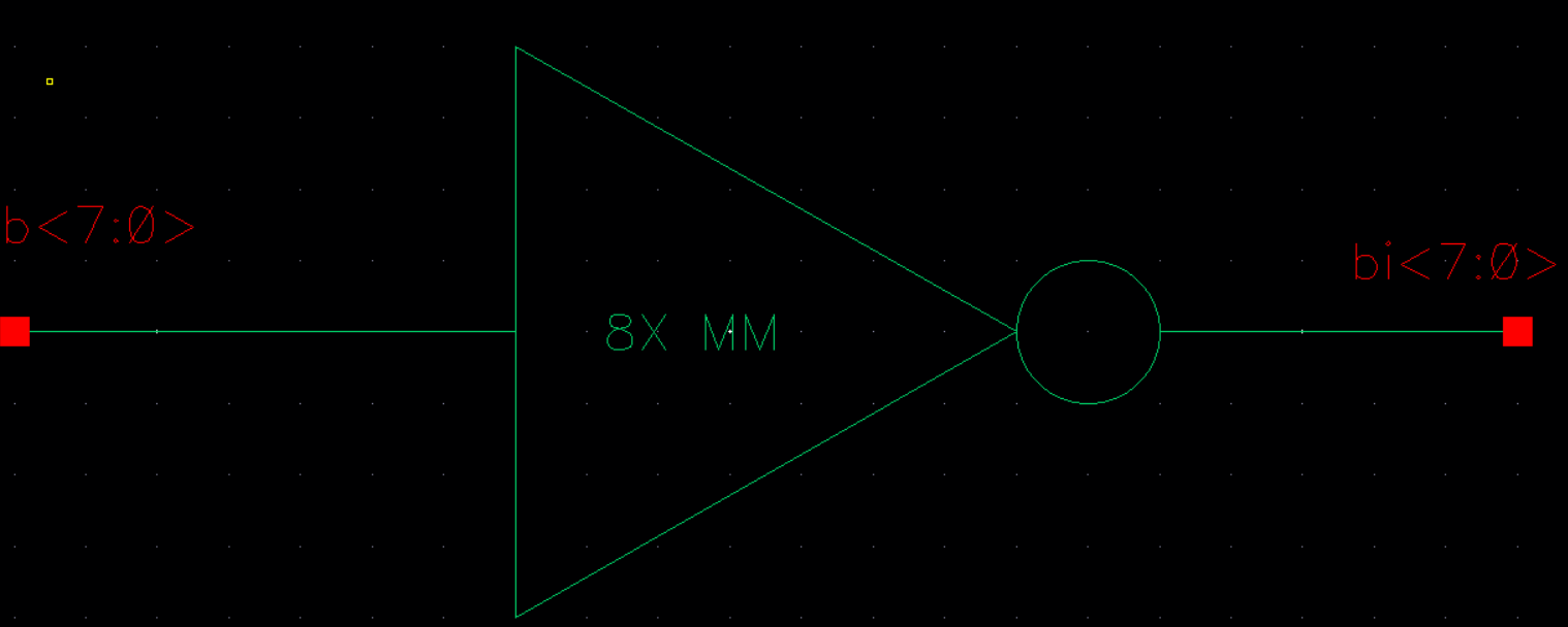
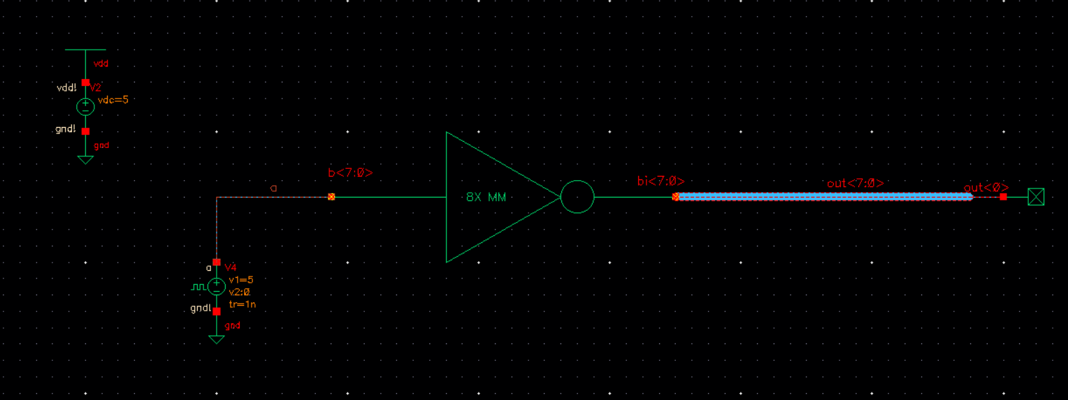
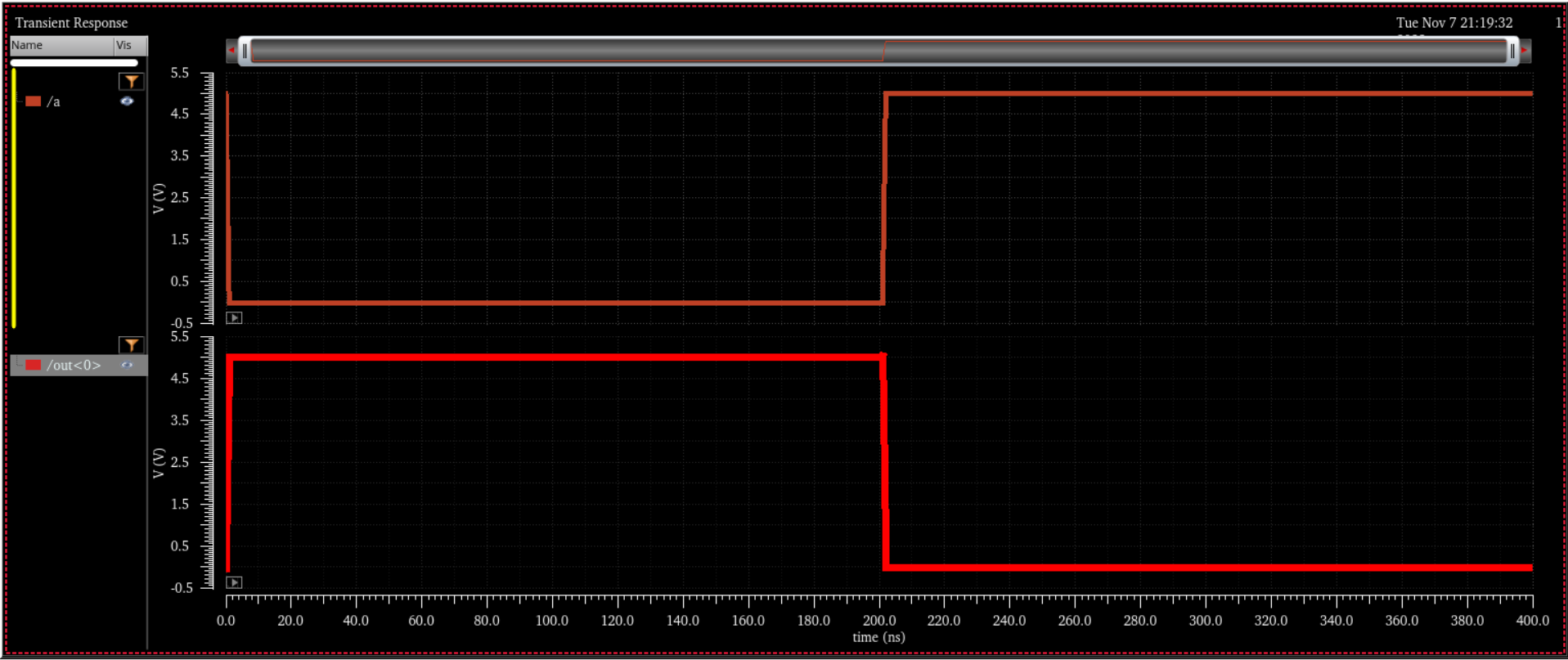
8-bit Inverter:
Schematic:
Symbol:
Simulation:
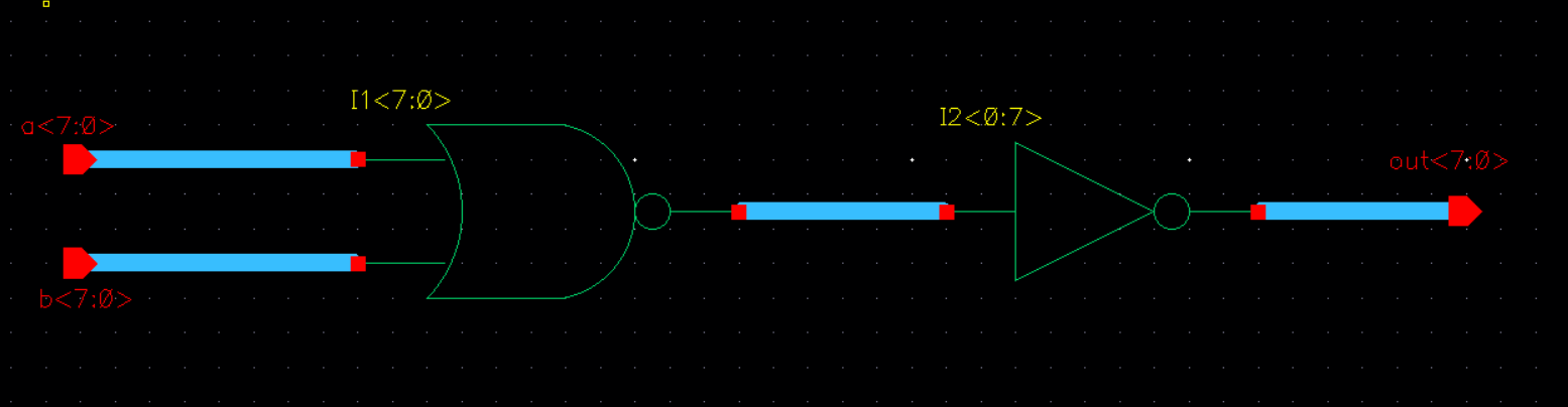
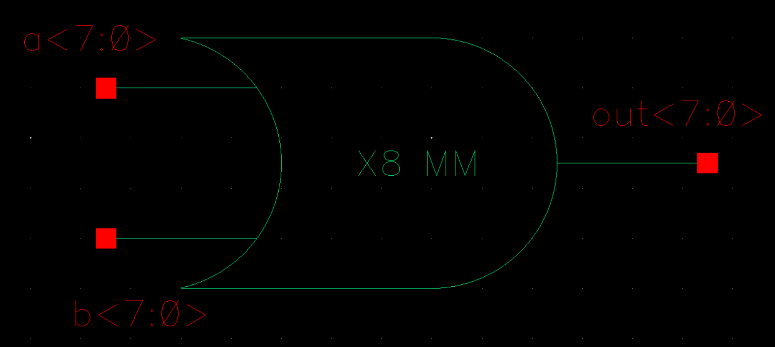
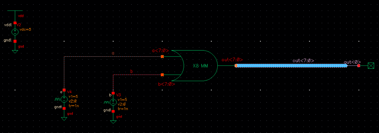
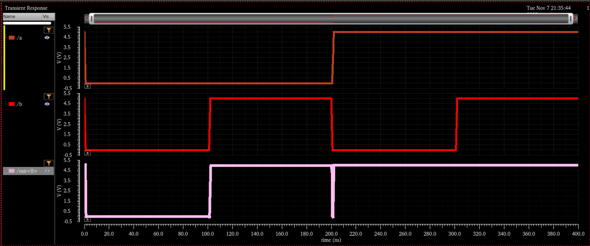
OR Gate:
Instead of creating a OR Gate from scratch, I added an inverter to the NOR Gate's output to make the OR Gate.
Schematic:
Symbol:
Simulation:
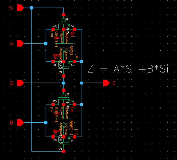
2-to-1 DEMUX/MUX
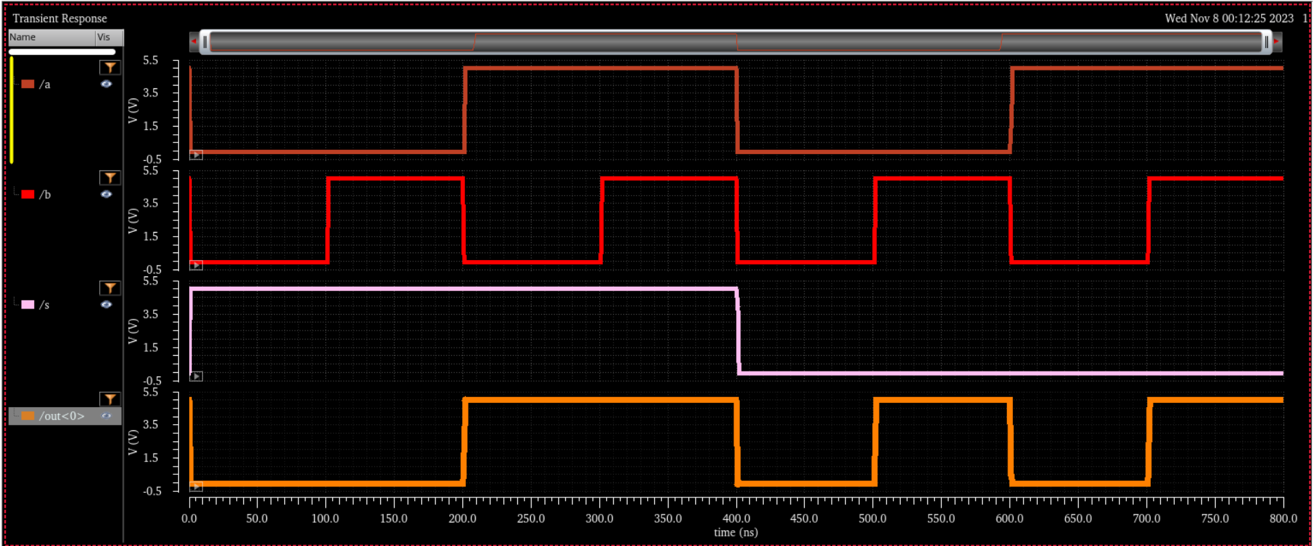
The 2-to-1 DEMUX/MUX will have four main inputs A, B, S and Si.
Si and S will select the line input.
If input S is high, then the input A will pass through to Z output.
If input S is low, then the input B will pass through to Z output.
Schematic:
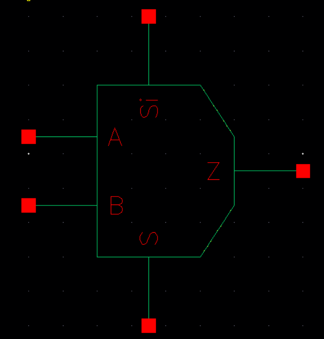
Symbol:
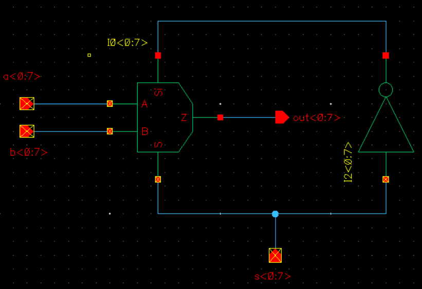
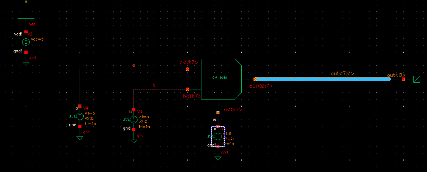
8-bit 2-to-1 DEMUX/MUX
Schematic:
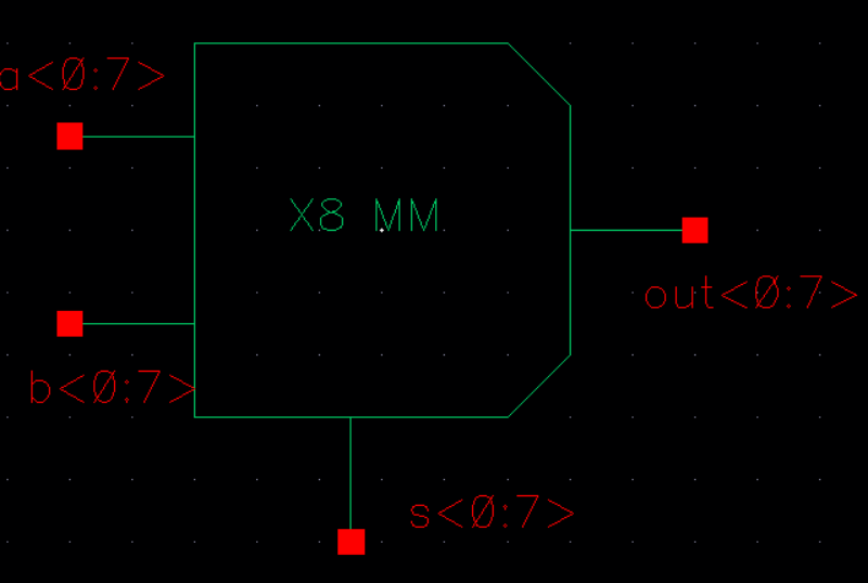
Symbol:
Simulation:
Return to EE421 Labs