Lab 6 - ECE 421L
Authored
by Martin Mercado mercam13@unlv.nevada.edu,
10/25/2023
Design, layout, and simulation of a CMOS NAND gate, XOR gate, and Full-Adder
Pre-lab work
- Back-up all of your work from the lab and the course.
- Go through Cadence Tutorial 4
- Read through the lab in its entirety before starting to work on it.
Tutorial 4:
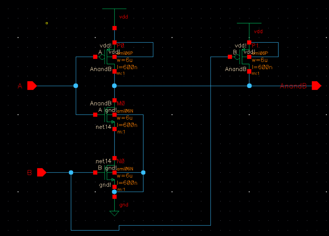
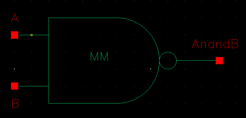
In this tutorial, I'll be designing, layout, and simulating the operation of a NAND gate.
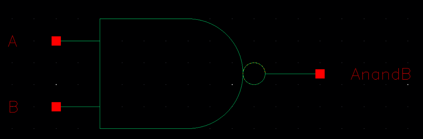
First, I'll be creating a schematic and symbol for a NAND gate.
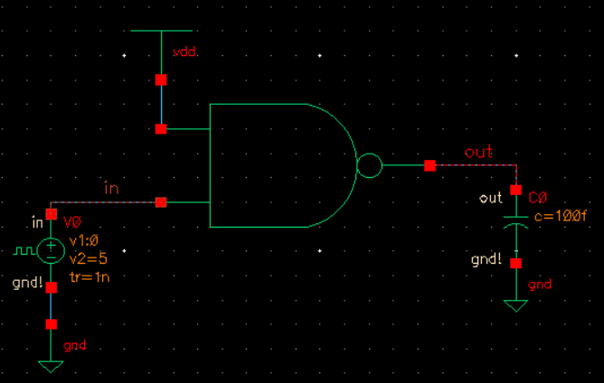
Next, I will simulate the operation of the gate.
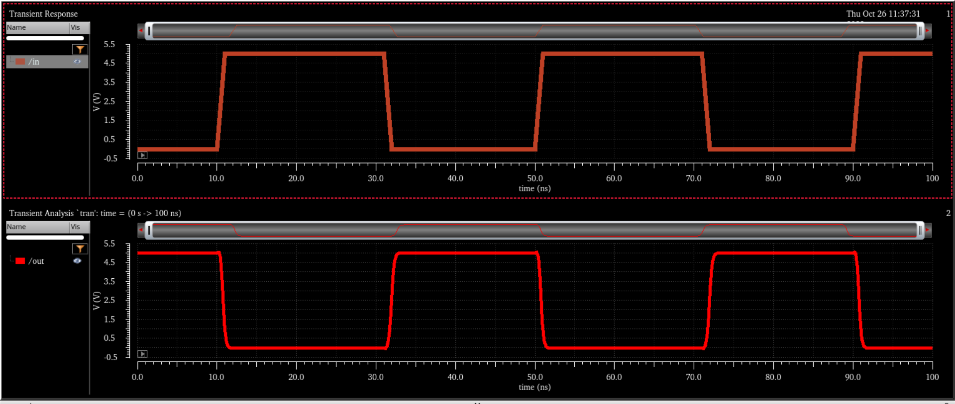
Net3 (Orange, Output) Net2 (Red, Input)
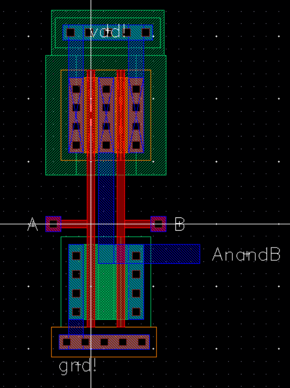
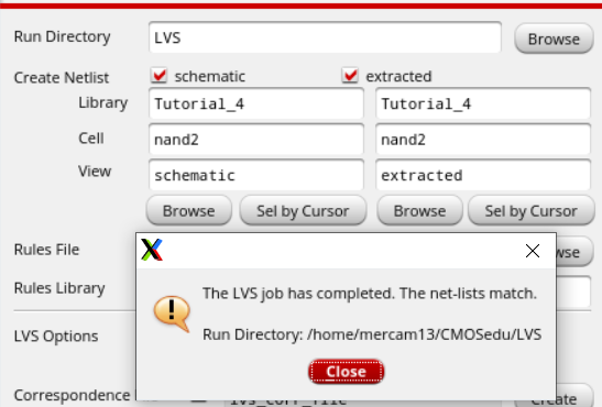
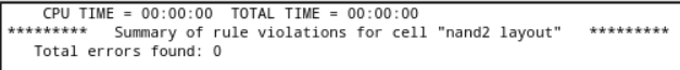
Now I will layout the NAND gate.
Also making sure to DRC and LVS.
______________________________________________________________________________________________________________________
Lab:
I will be doing a design, layout, and simulation of a NAND gate, XOR gate and Full-Adder for this lab.
2-Input NAND gate:
I will be using the NAND gate created in the pre-lab.
Simulate the NAND gate with 2-Inputs.
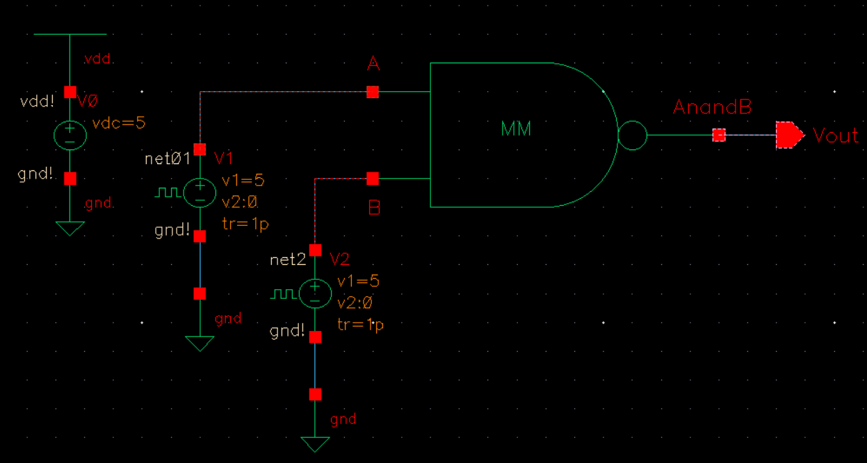
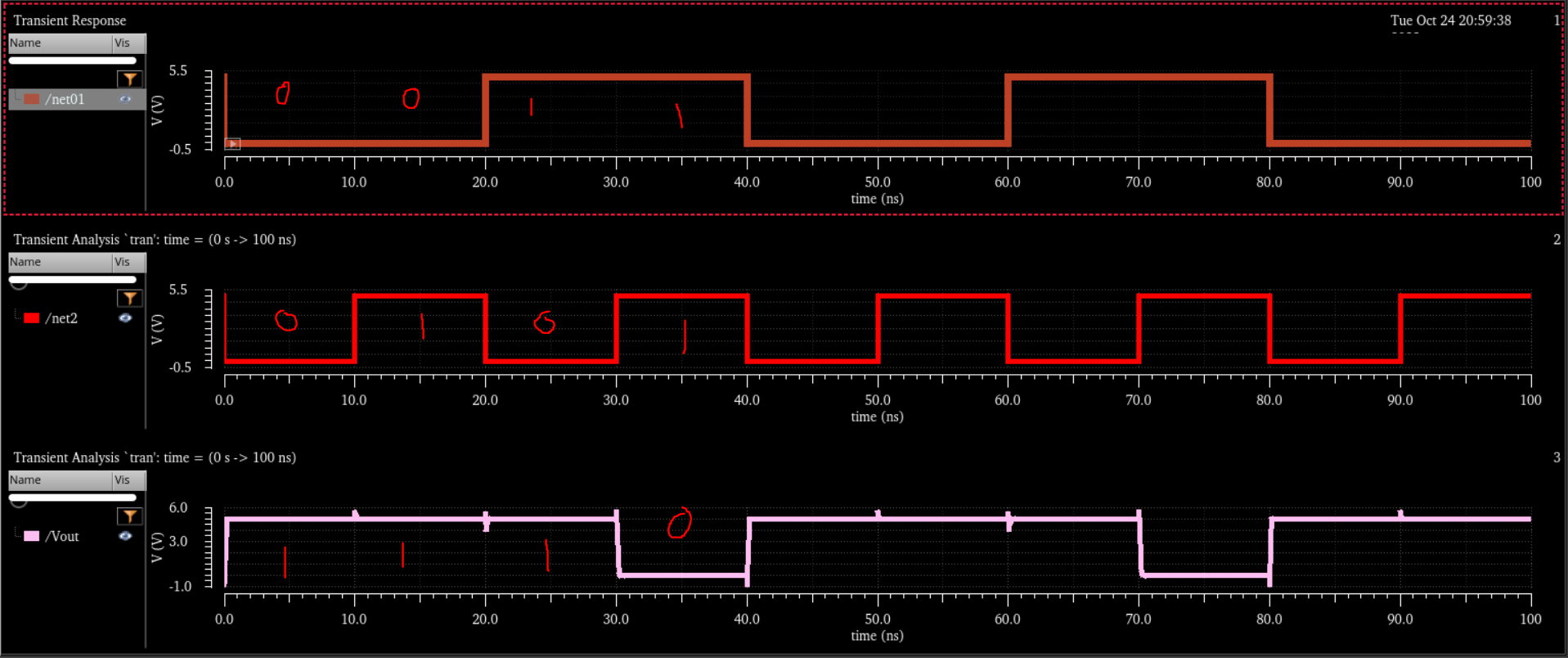
Net1 (A) Net (B) Vout(
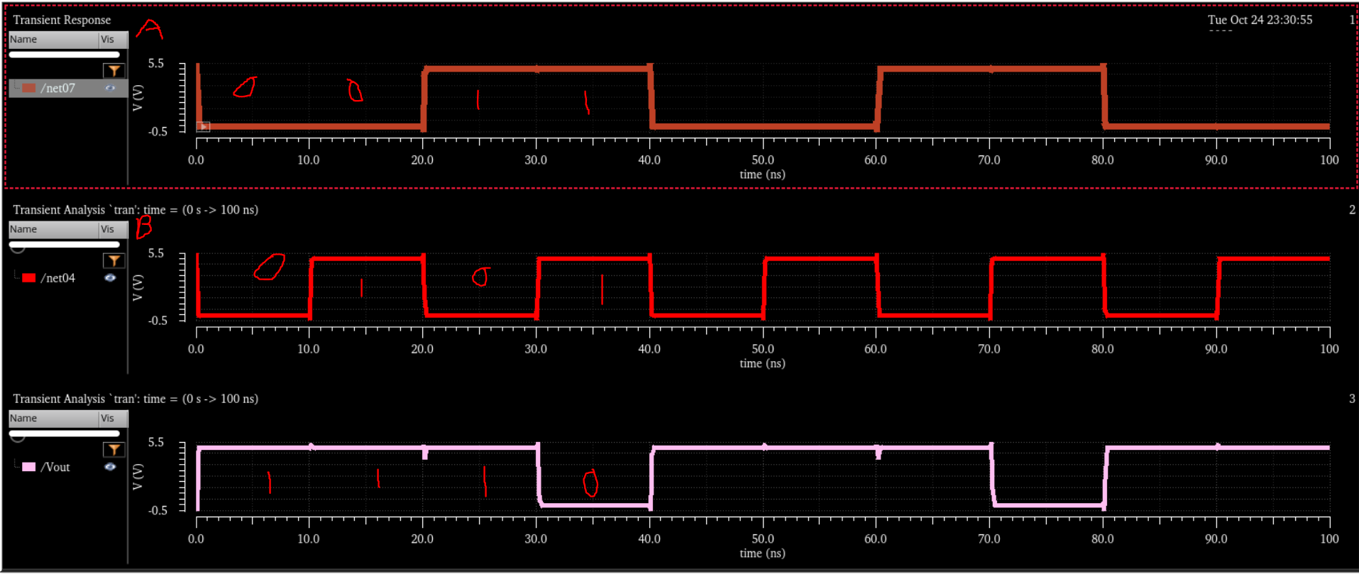
The plot above represents the truth table of the NAND gate.
The output has some noise in between signals.
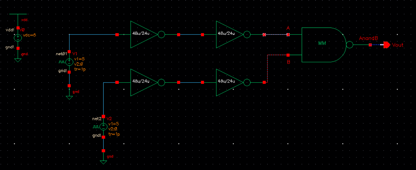
I will be using inverters to minimize the noise.
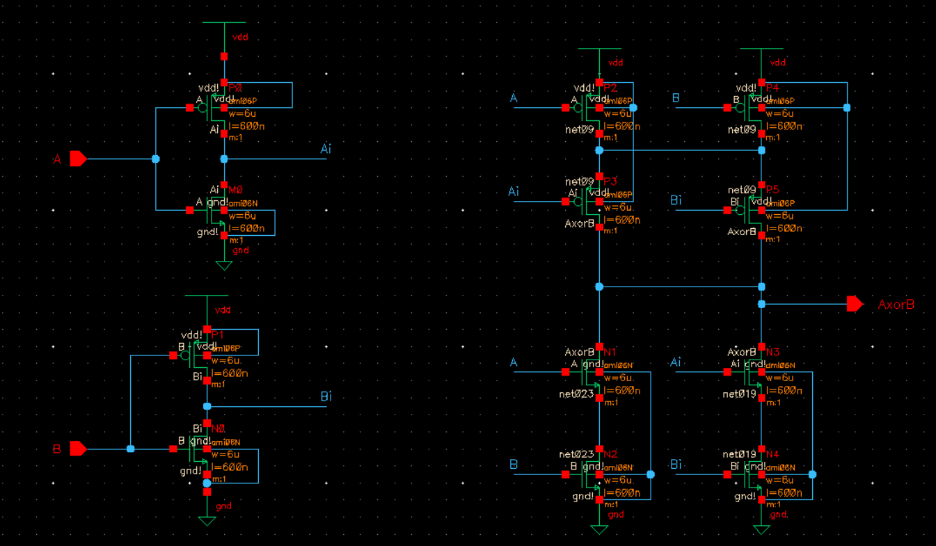
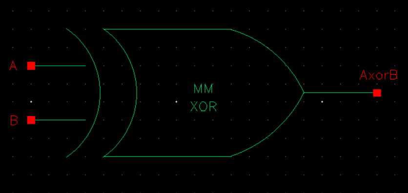
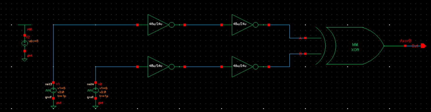
2-Input XOR Gate:
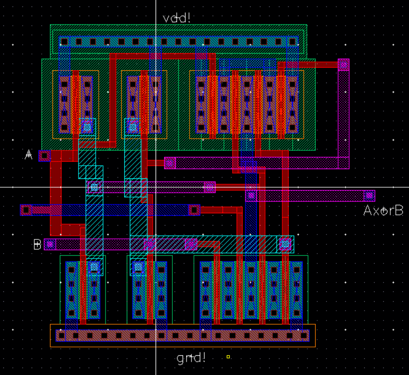
I will be making a schematic, symbol and layout of a XOR Gate.
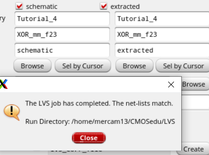
Also DRC and LVS the layout.

Next is to simulate the XOR Gate with 2-Inputs.
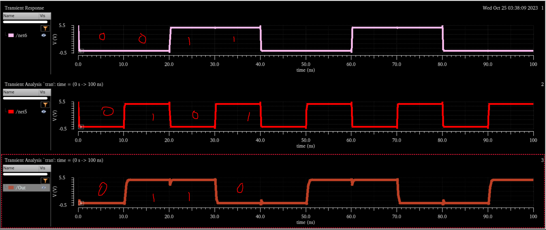
The Plot above shows the truth table of the XOR Gate.
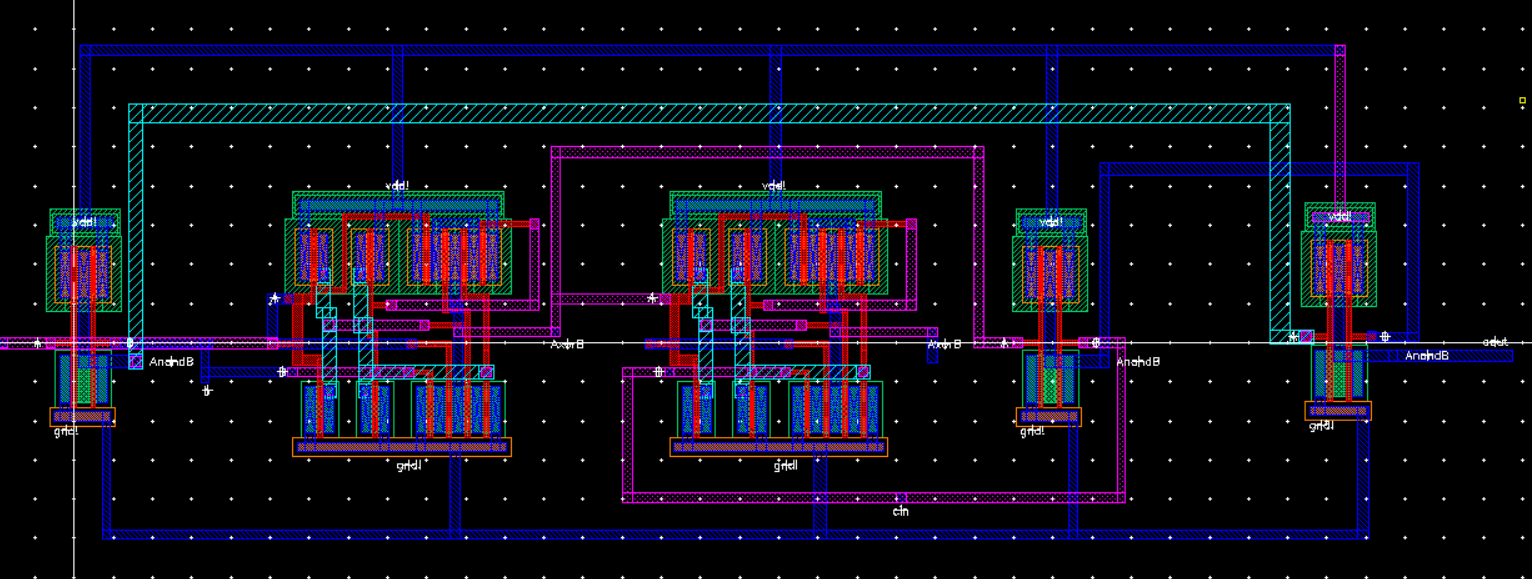
Full Adder:
Using the symbols of the NAND gate and XOR gate, I will create a schematic of a Full Adder.
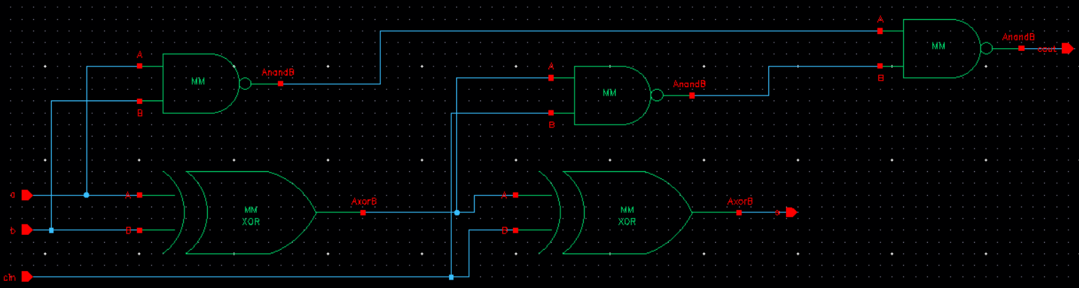
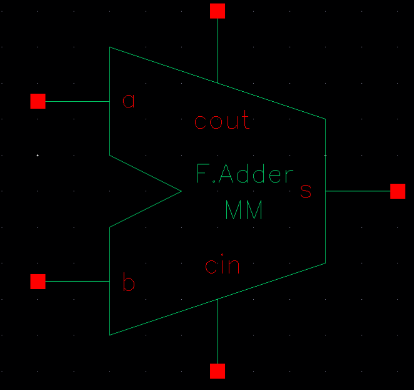
Symbol:
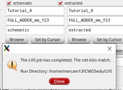
Layout with DRC and LVS:

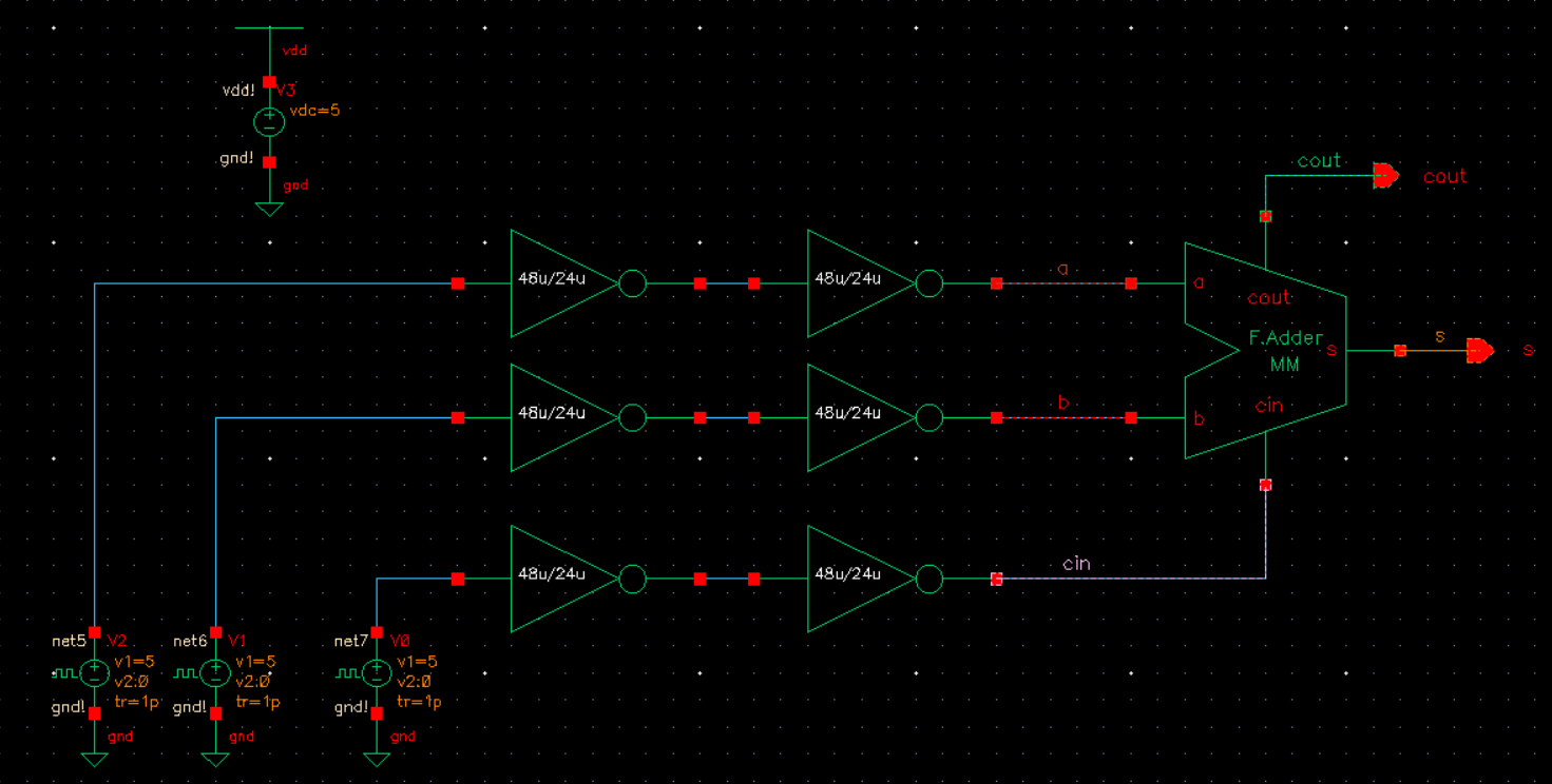
Next, I will be simulating the Full Adder:
Schematic:
Plots:
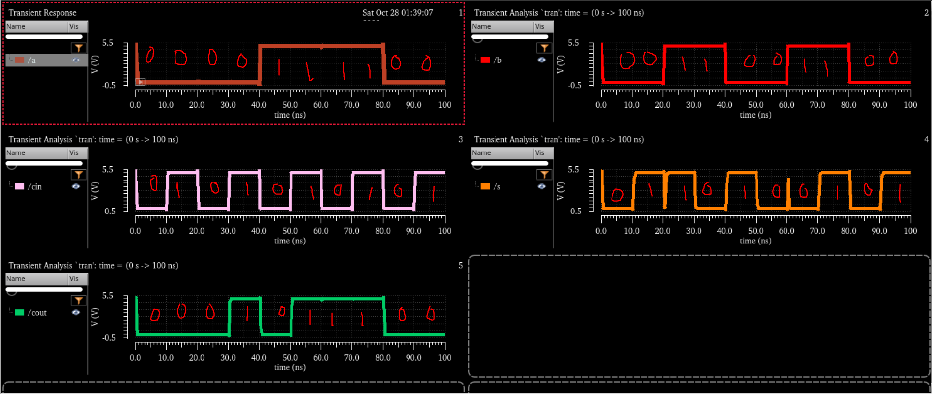
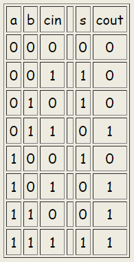
The plot above matches the given table below, so the Full Adder works.
End of Lab
______________________________________________________________________________________________________________________
Back-up of Files

Return to EE421 Labs