
Lab 5 - ECE 421L
Design, Layout, and Simulation of a CMOS Inverter
Pre-Lab:
Tutorial 3:
1. What does the Bindkey q do?
Object Properties
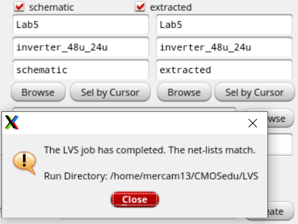
2. Which two Cell Views are used when doing an LVS?
Schematic and Extracted
3. What is the difference between the nmos and nmos4 schematic cells?
Nmos4 has 4 terminals (body/bulk)
4. How do you select the MOSFET models in the ADE window? What does ADE stand for?
Analog Design Environment
5. What is the difference between moving and stretching?
Moves the object, Stretches the object
6. How do you layout a rectangle on the metal1 layer?
Check m1 and press R to create a rectangle
7. What does the ! indicate at the end of gnd! and vdd!
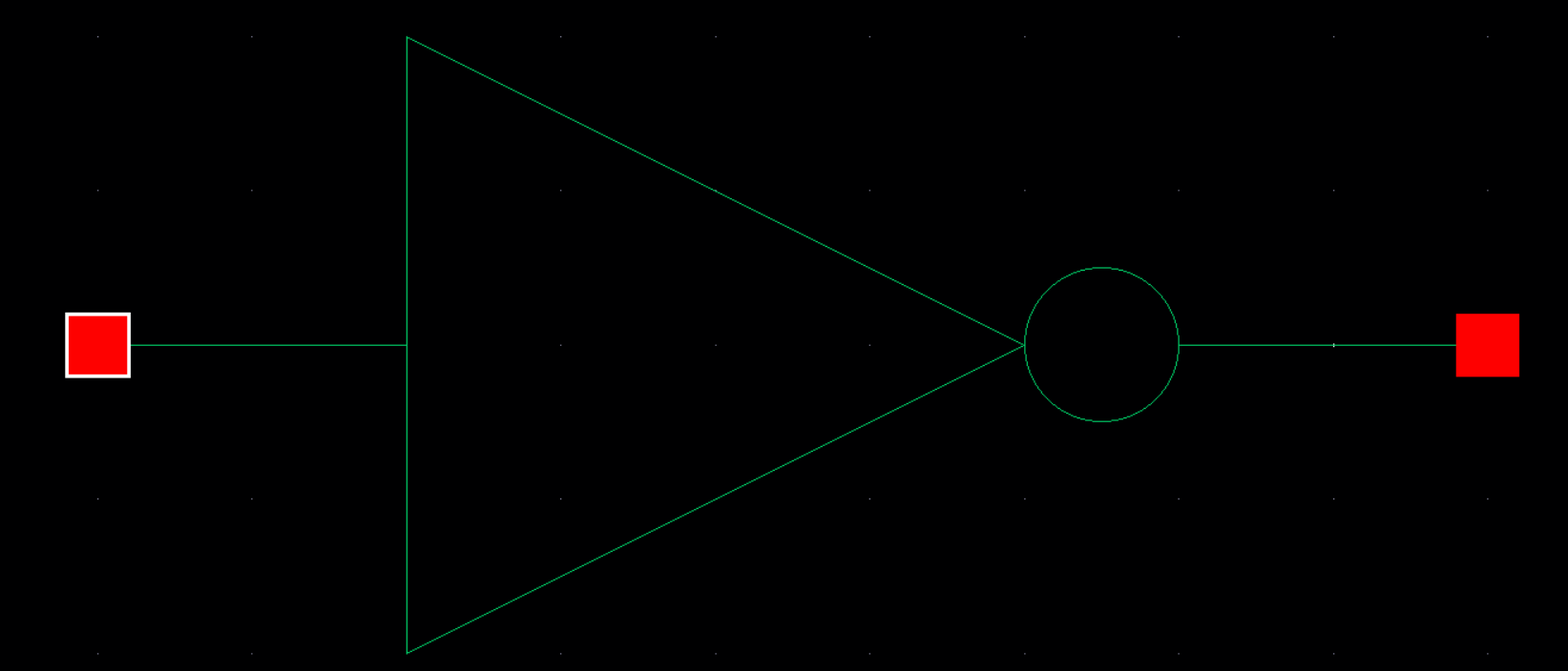
Global
8. What do the acronyms LSW and CIW stand for?
Layer Select Window, Command Interpreter Window
9. How is the ruler used? Cleared?
Press K to use ruler, Clear with delete or Press U to undo
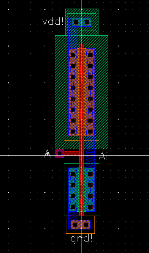
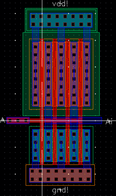
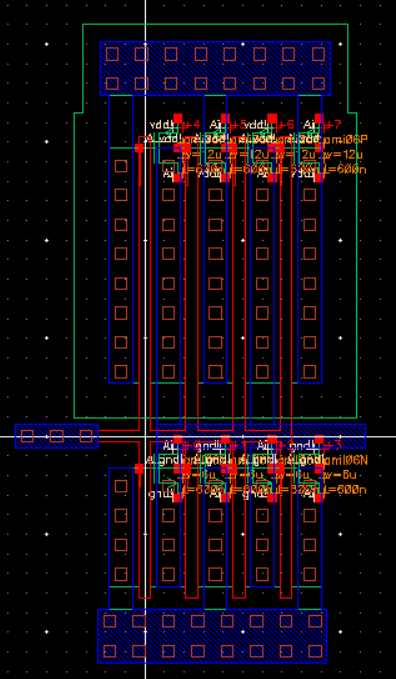
Then I will create a layout.
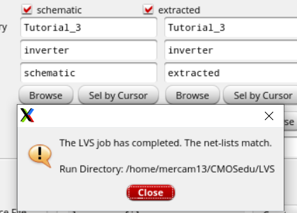
DRC, Extract, and LVS.
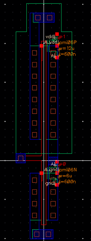

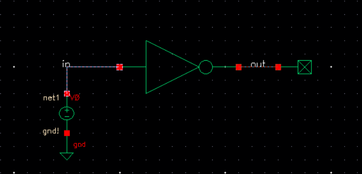
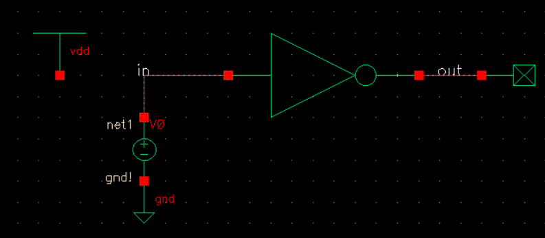
In (Green) Out (Blue)
With Voltage
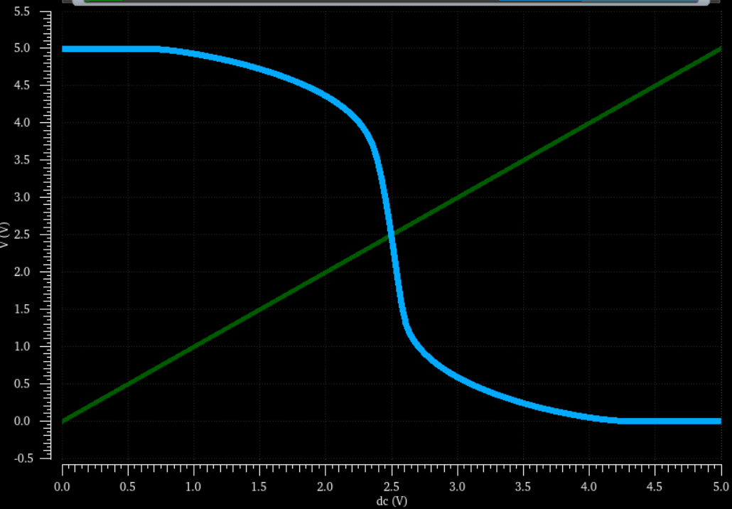
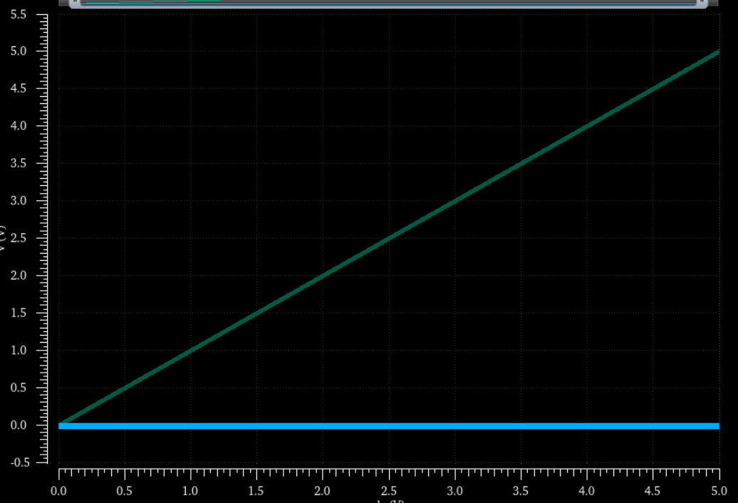
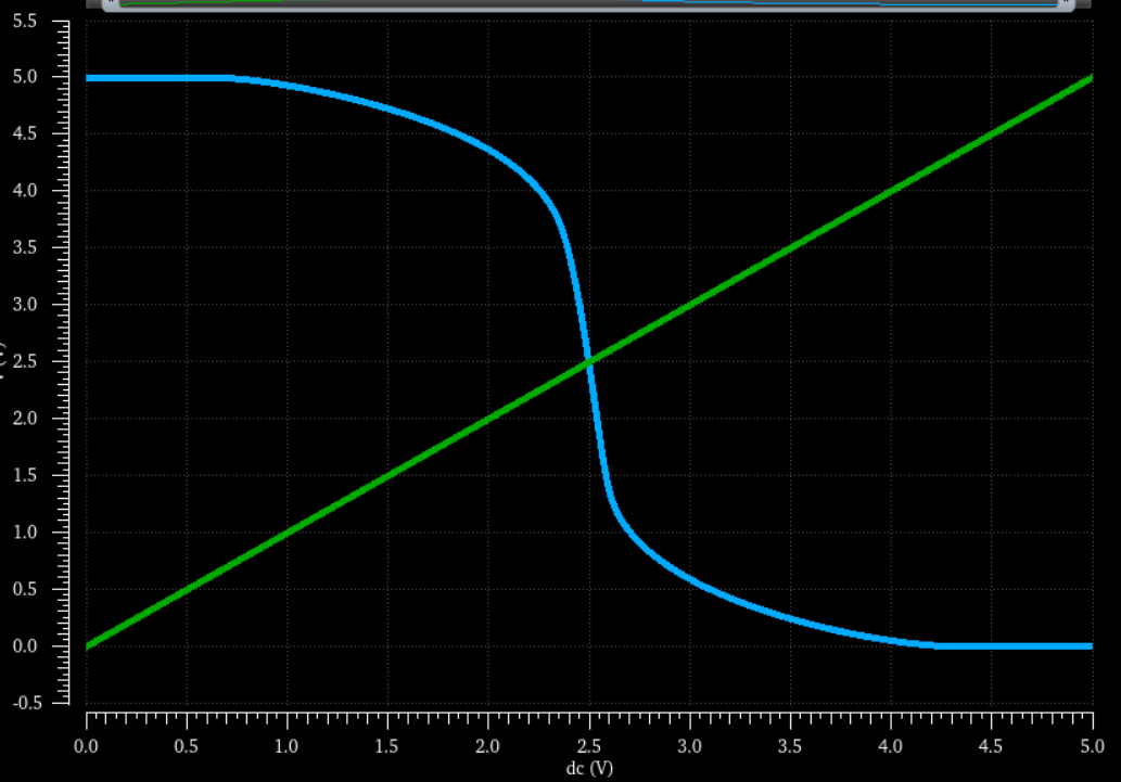
Now I will simulate the extracted, which should result with the same plot.
_____________________________________________________________________________________
Lab:
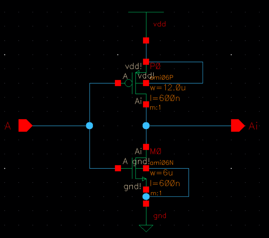
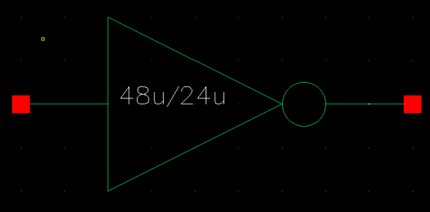
I will be creating 12u/6u and 48u/24u inverter.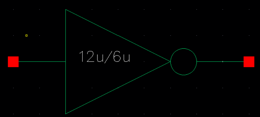
LVS
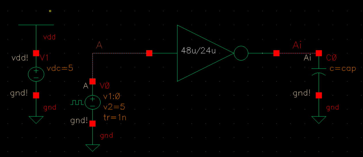
48u/24u Inverter: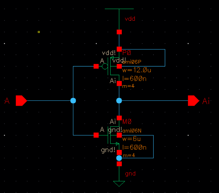

DRC
LVS
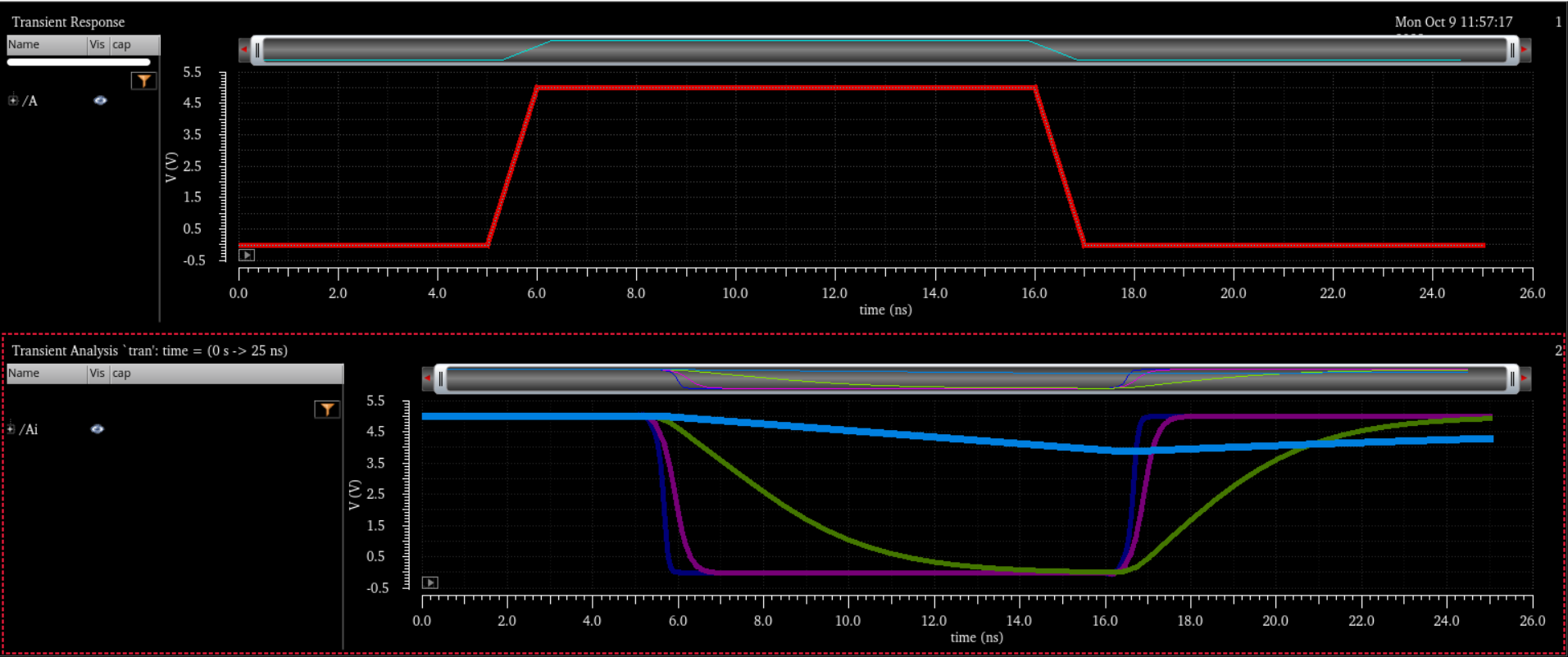
Now I will simulate both inverters driving a 100fF, 1 pF, 10 pF, and 100pF capacitive load.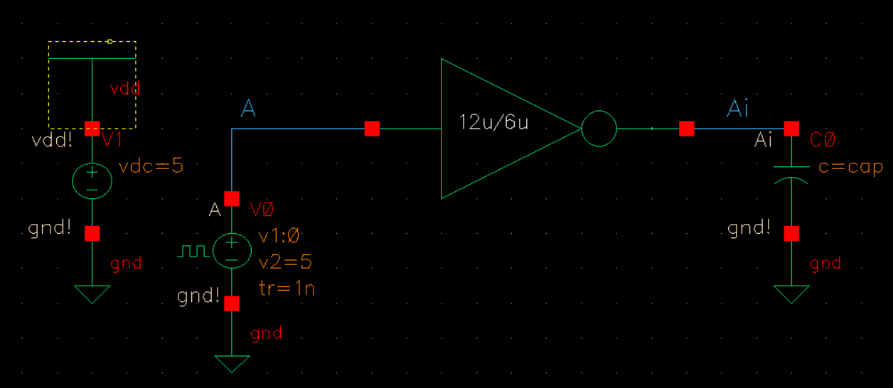
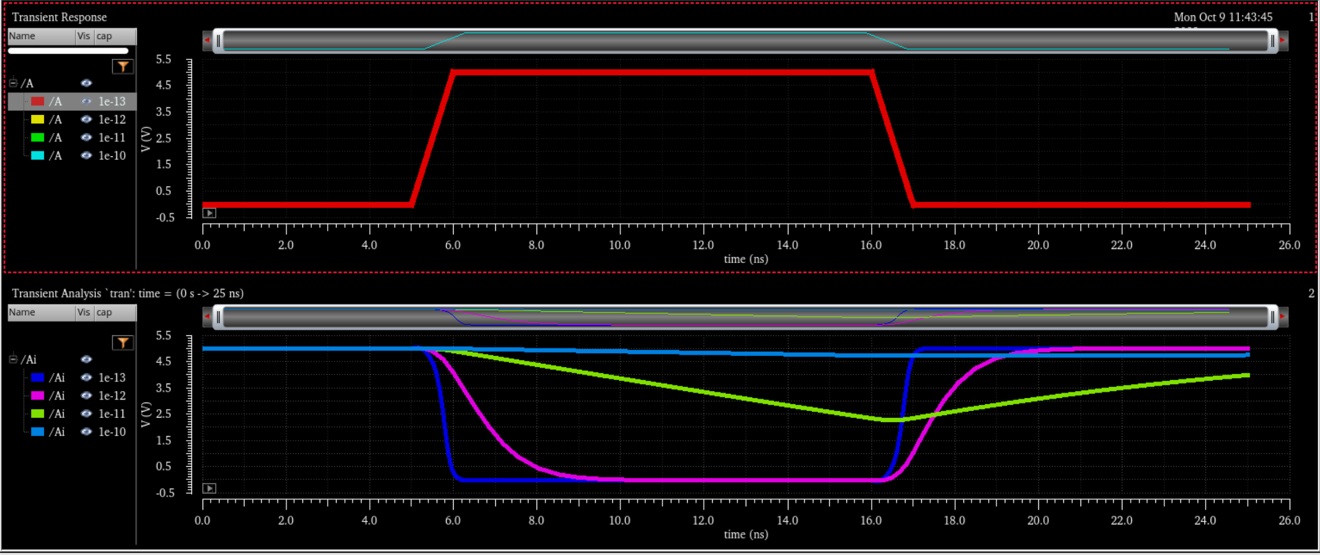
Simulation
100fF(Blue) 1pF(Purple) 10pF(Green)
Simulation
100fF(Blue) 1pF(Purple) 10pF(Green)
Ultrasim:
I will try simulating with UltraSim.
12u/6u Inverter:
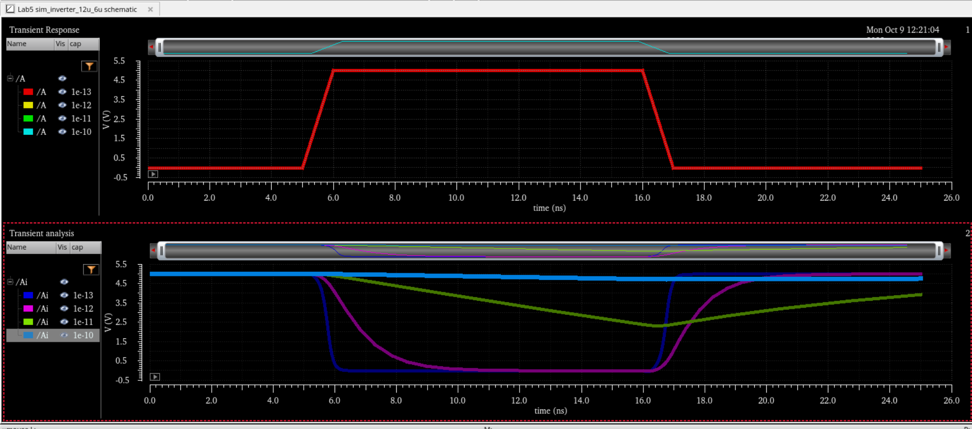
Simulation
100fF(Blue) 1pF(Purple) 10pF(Green)
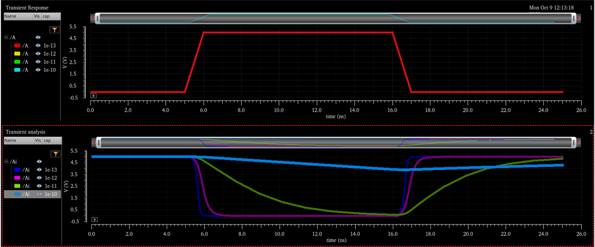
Simulation
100fF(Blue) 1pF(Purple) 10pF(Green)