Lab 3 - ECE 421L
Authored
by Martin Mercado mercam13@unlv.nevada.edu,
09/19/2023
Layout of a 10-bit digital-to-analog converter (DAC)
Pre-lab:
- Back-up all of my previous work from the lab and the course
- Finish Tutorial 1

Tutorial 1:
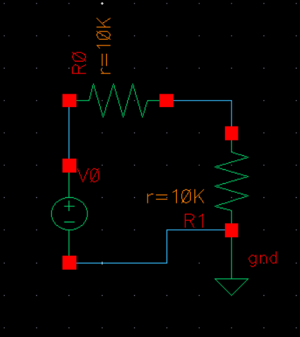
I left off with creating the schematic and simulating the 10k voltage divider.
Next, I will be making a symbol for the voltage divider.
First I will need to add pins in and out.
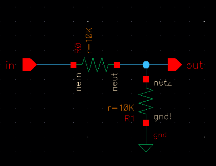
Then I will create a symbol of the schematic after verifying and checking.

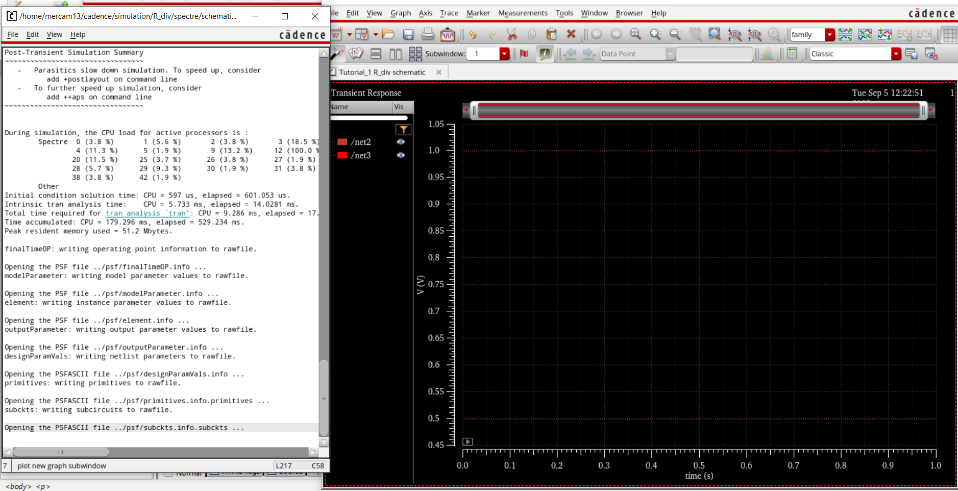
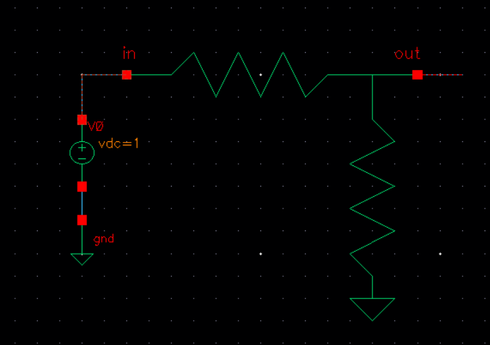
Now I will verify that the symbol works by simulating it.
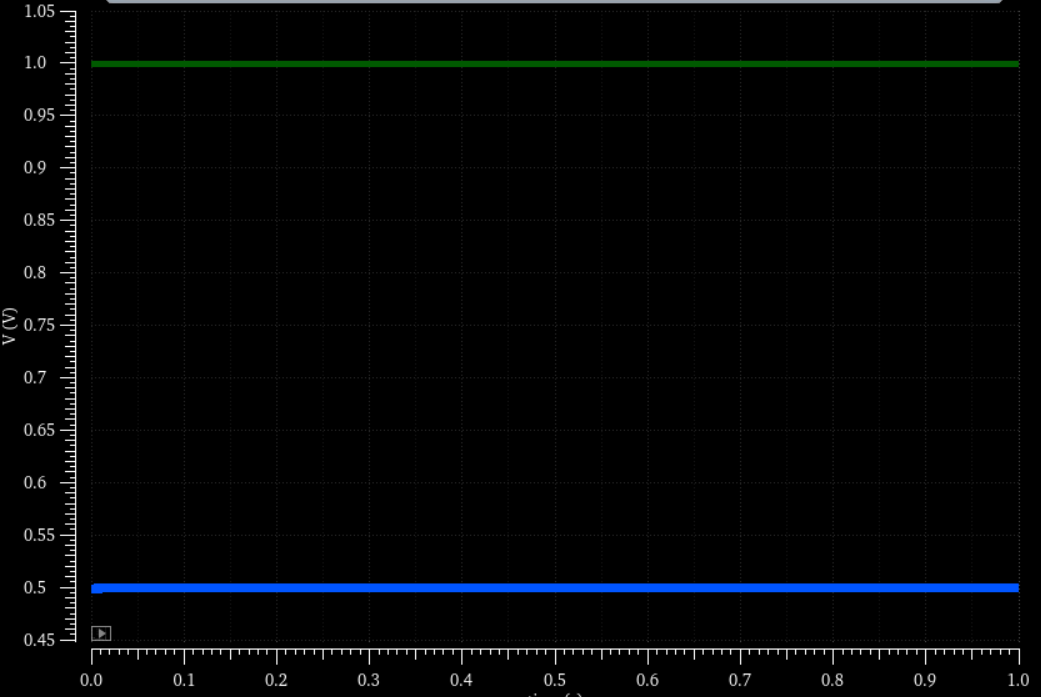
The plot confirms that the symbol works when compared to the other plot above.
Now I am ready to lay out a resistive divider.
Before I lay out the resistive divider I will be making an n-well resistor.
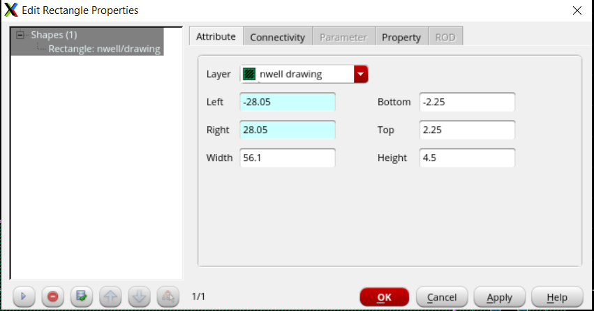
I will need to calculate the parameters of the 10k n-wll using Rsheet x (L/W).
800 x (L/W)=10k (C5 process is roughly 800 ohms = Rsheet)
Minimum width of an n-well is 3.6um so I will choose a width of 4.5um and a length of 56um.
Snap spacing is set to 0.15um so 56/.15 = 373.33 which is no good, so I have to set it to 56.1 um 56/.15 = 374 (whole number).
4.5/.15 = 30 which is good for width.
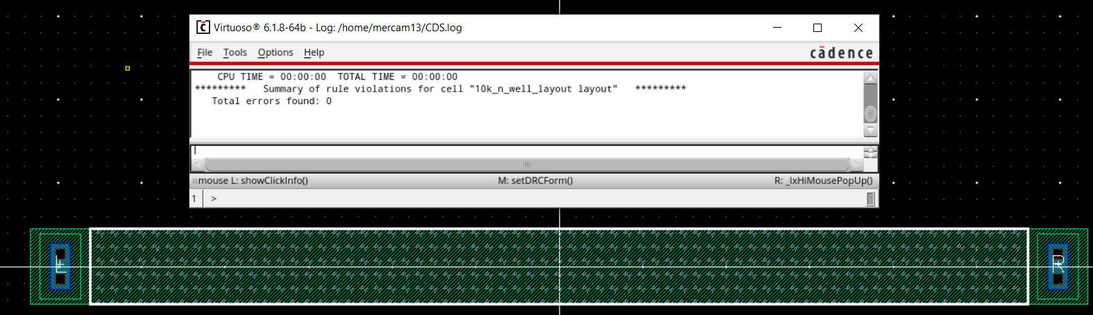
Now I am ready to make the n-well layout.
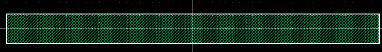
Before adding the n-taps and metal I will DRC the layout.

Now I will add the n-taps and metal (connections) and res_id then DRC.
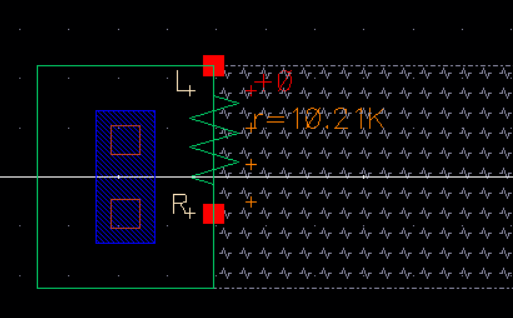
Next, I am going to extract the n-well layout and confirm its resistance.
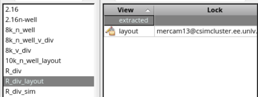
Now I am going to draw the layout of the R_div cell and DRC after connecting the pins of the resistors.
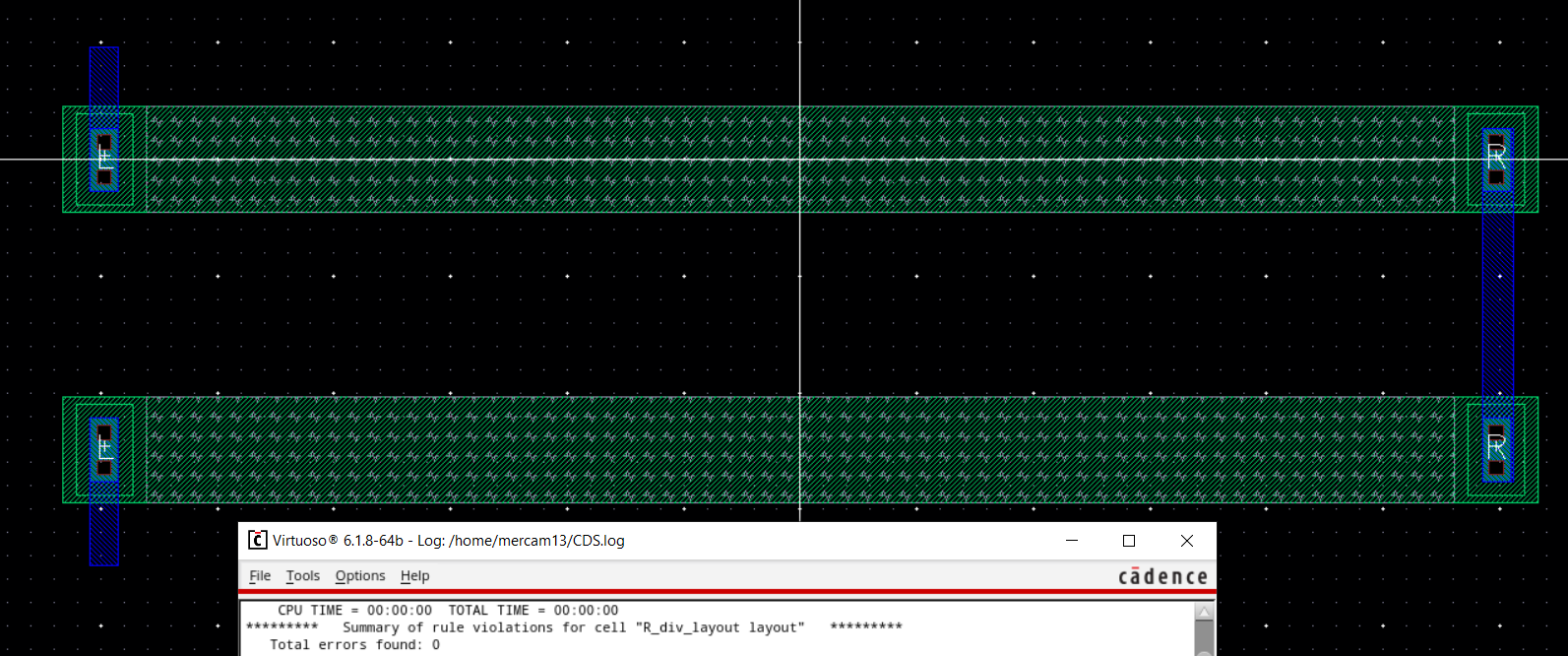
Next add pins on the metal layer named in, out, and gnd then DRC.
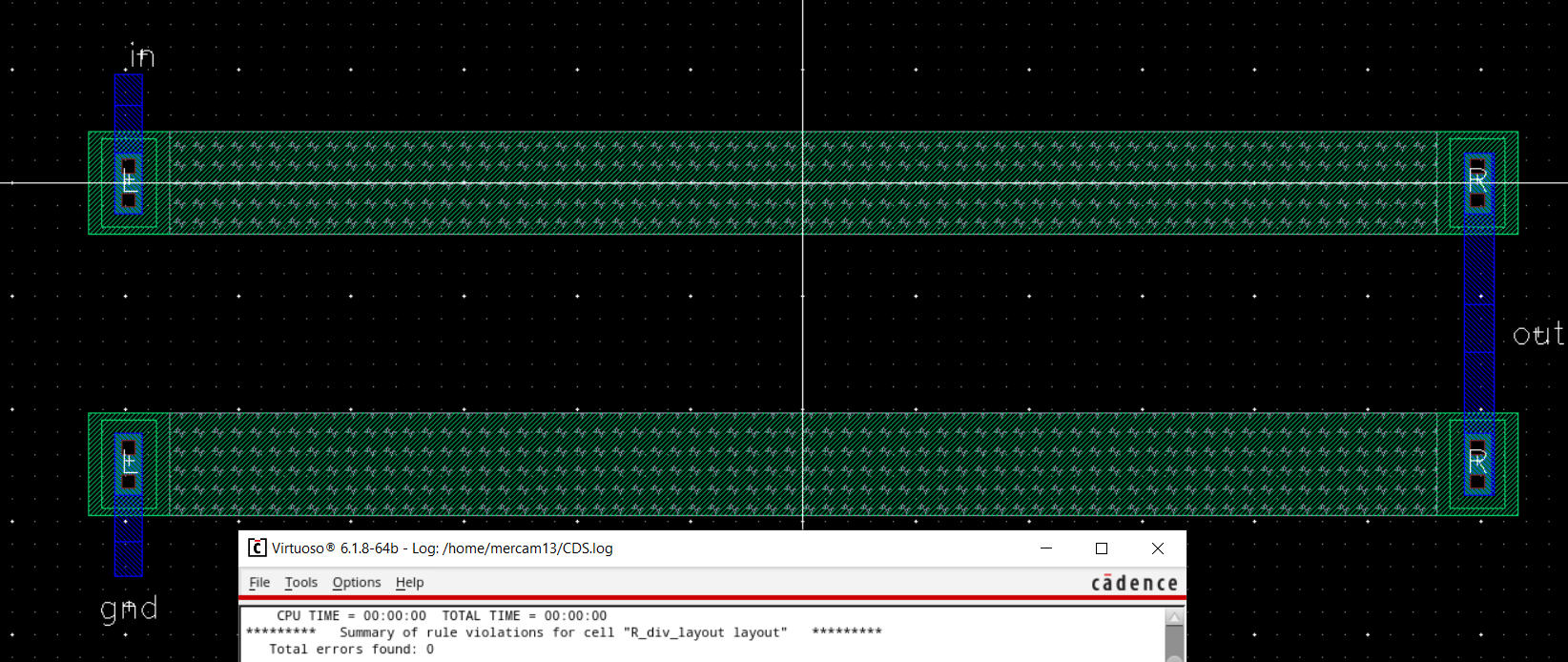
Extract and LVS.
That concludes Tutorial 1 and pre-lab
Lab:
In this lab, I will be using the 10k nwell resistor I created to design a 10-bit DAC that follows the schematic from lab 2.
The parameters and DRC of the nwell resistor
800 x (L/W)=10k (C5 process is roughly 800 ohms = Rsheet)
Minimum width of an n-well is 3.6um so I will choose a width of 4.5um and a length of 56um.
Snap spacing is set to 0.15um so 56/.15 = 373.33 which is no good, so I have to set it to 56.1 um 56/.15 = 374 (whole number).
4.5/.15 = 30 which is good for width.
Now I will layout the DAC using the 10k resistor.
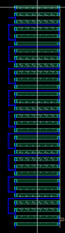
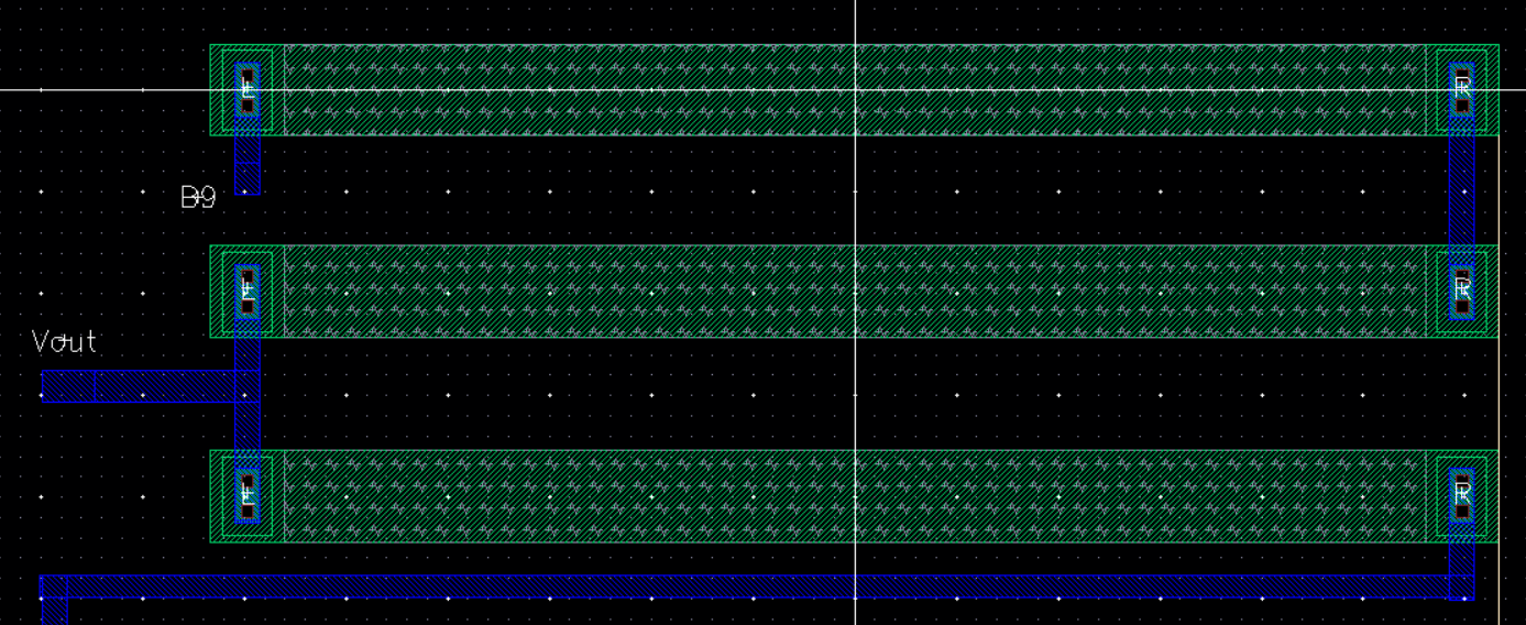
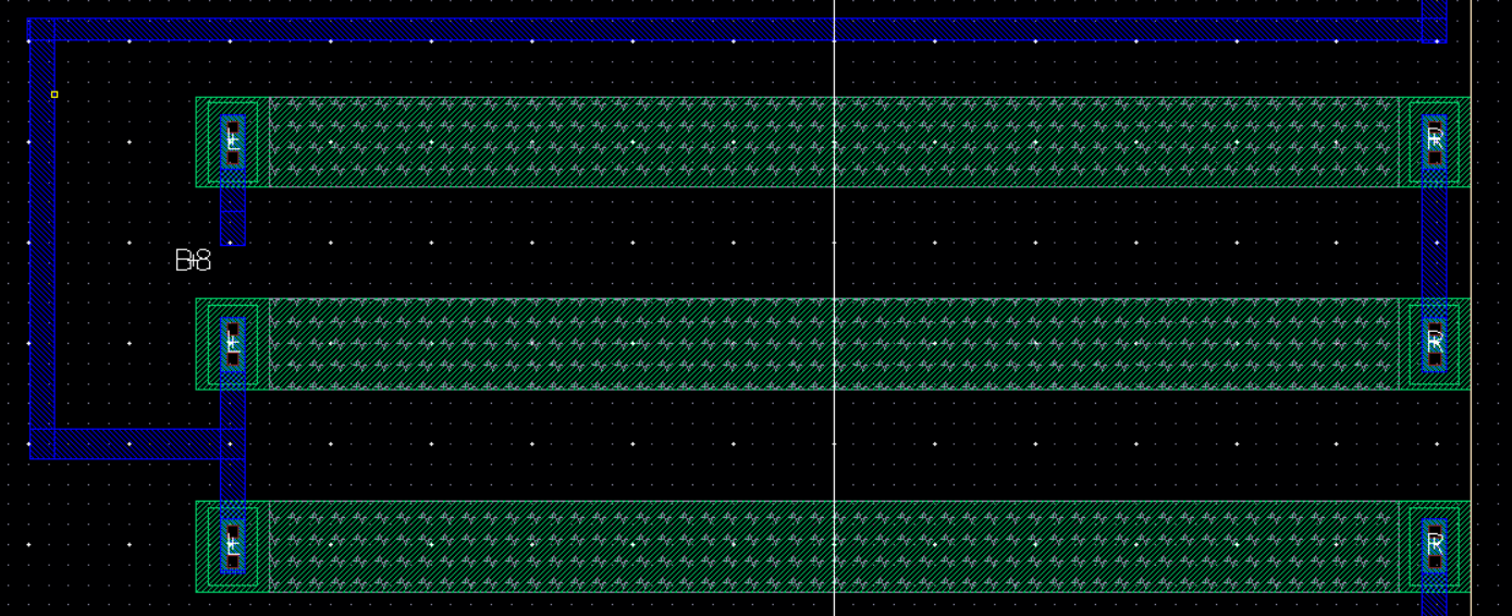
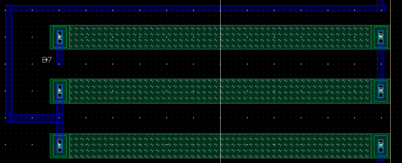
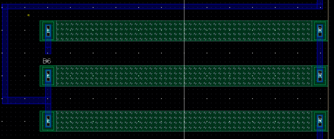
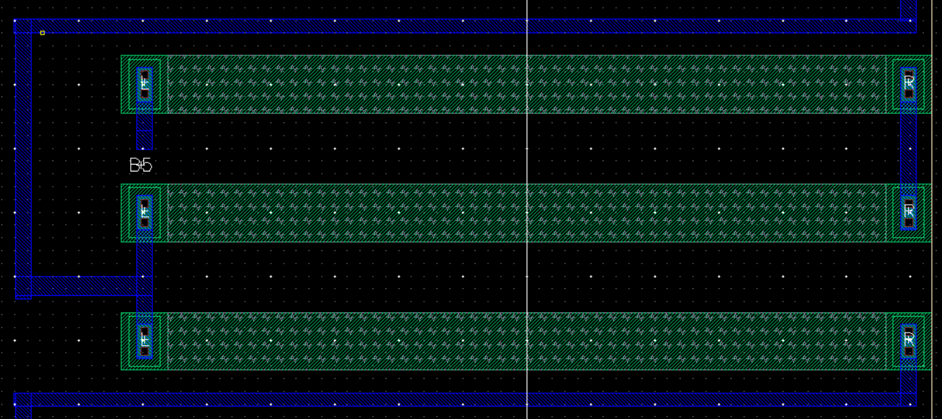
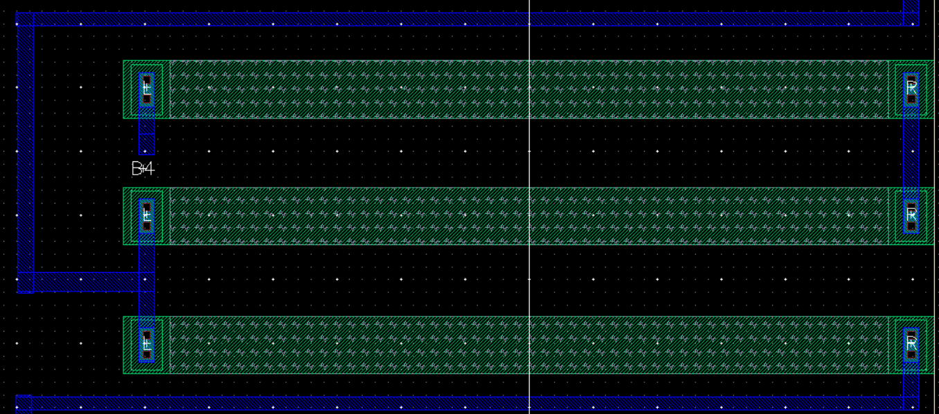
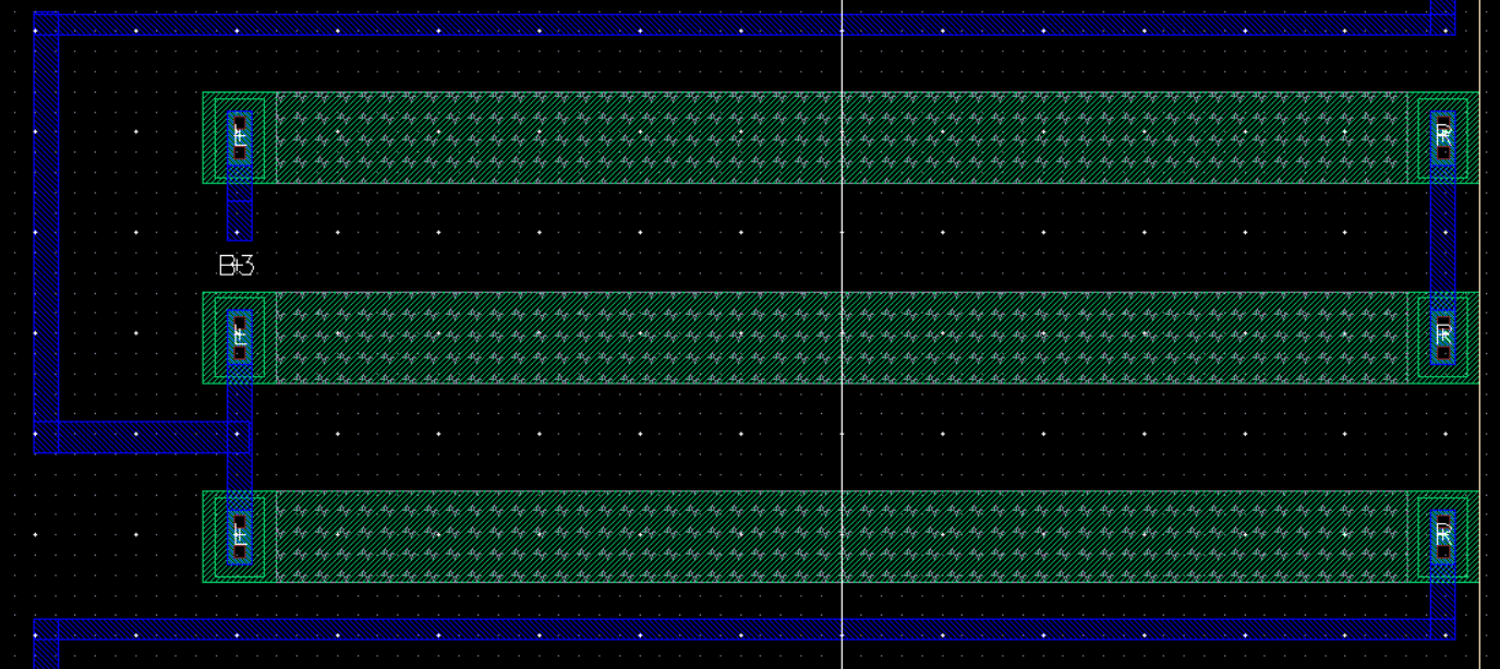
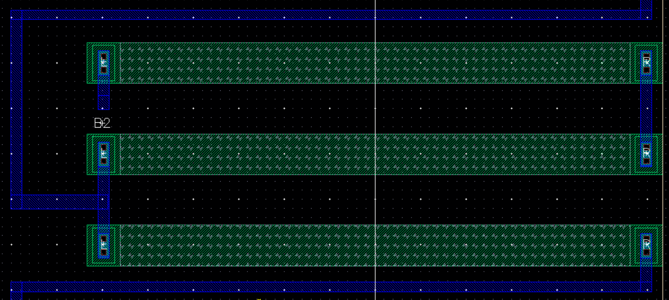
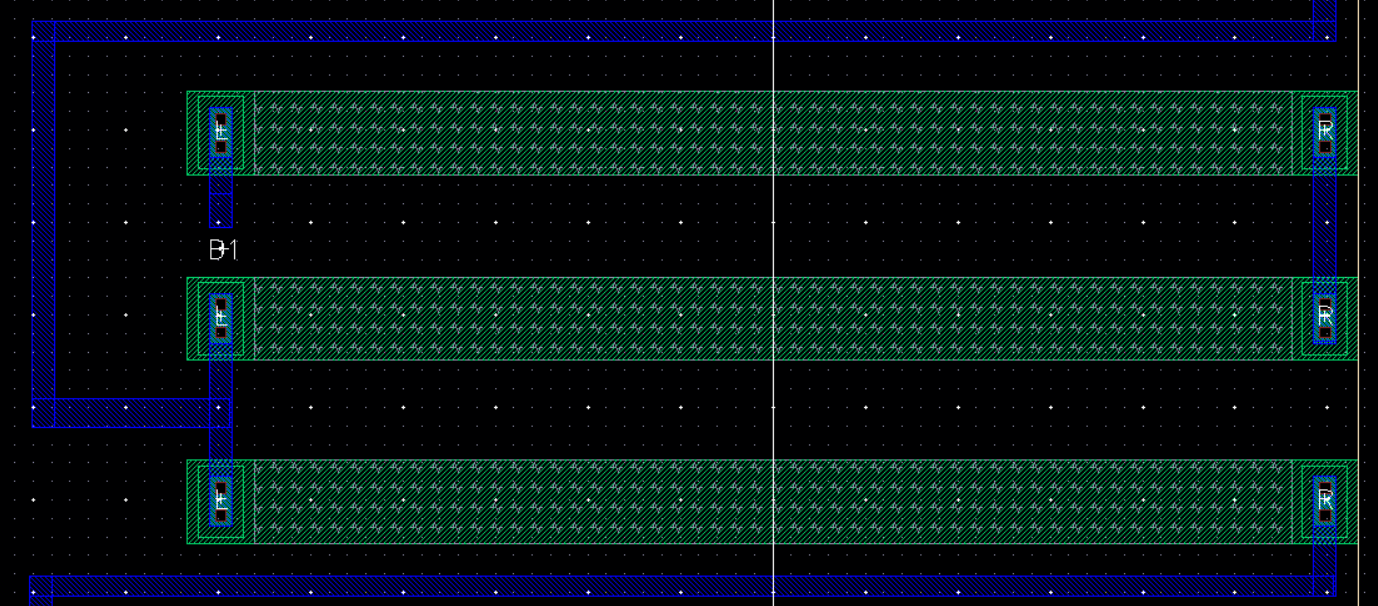
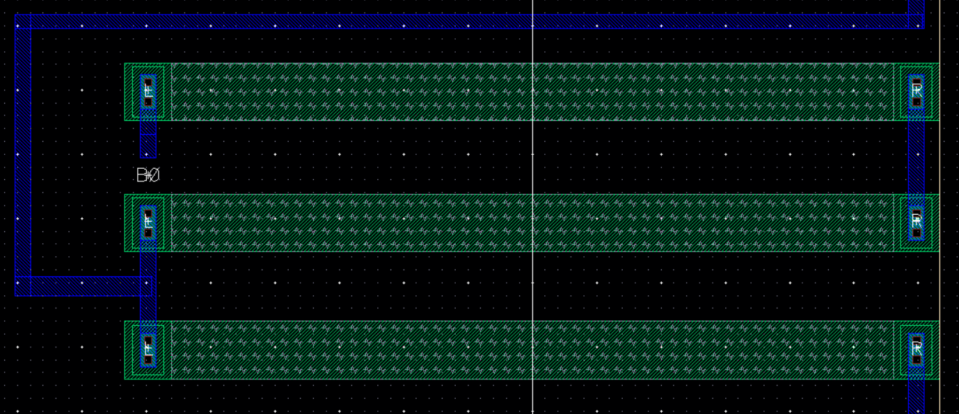
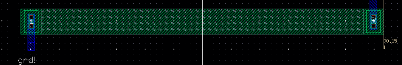
DRC check
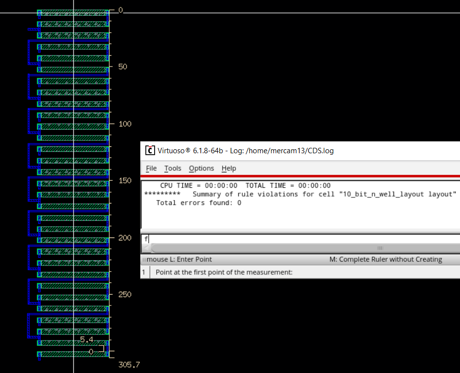
All resistors must be in the same x-axis but varying y-axis.
I can use a ruler (shortcut "K") to verfiy the distance .
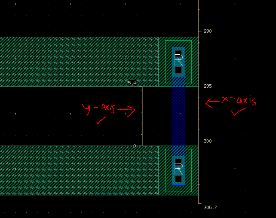
The ruler on the right confirms they are all in the same x-axis due to it being a straight line top to bottom.
The ruler on the left confirms that the resistors far enough apart in the y-axis.
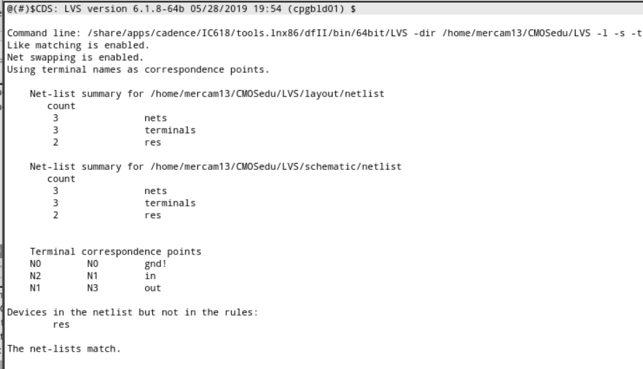
Finally, I LVS and see if it matches.

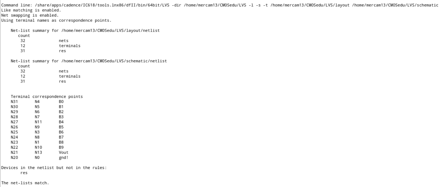
LVS confirms match.
Lab 3 Schematic and Layout Zip
Return to EE421 Labs