Lab 2 - ECE 421L
Authored
by Martin Mercado mercam13@unlv.nevada.edu,
09/13/2023
Design of a 10–bit digital–to–analog converter (DAC)
Pre-Lab:
- Back-up all of your work from the lab and the course.
- Read through this entire lab write-up before doing the pre-lab
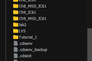
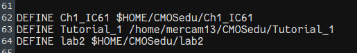
I downloaded lab2.zip, upload it to my directory and define it in my cds.lib.

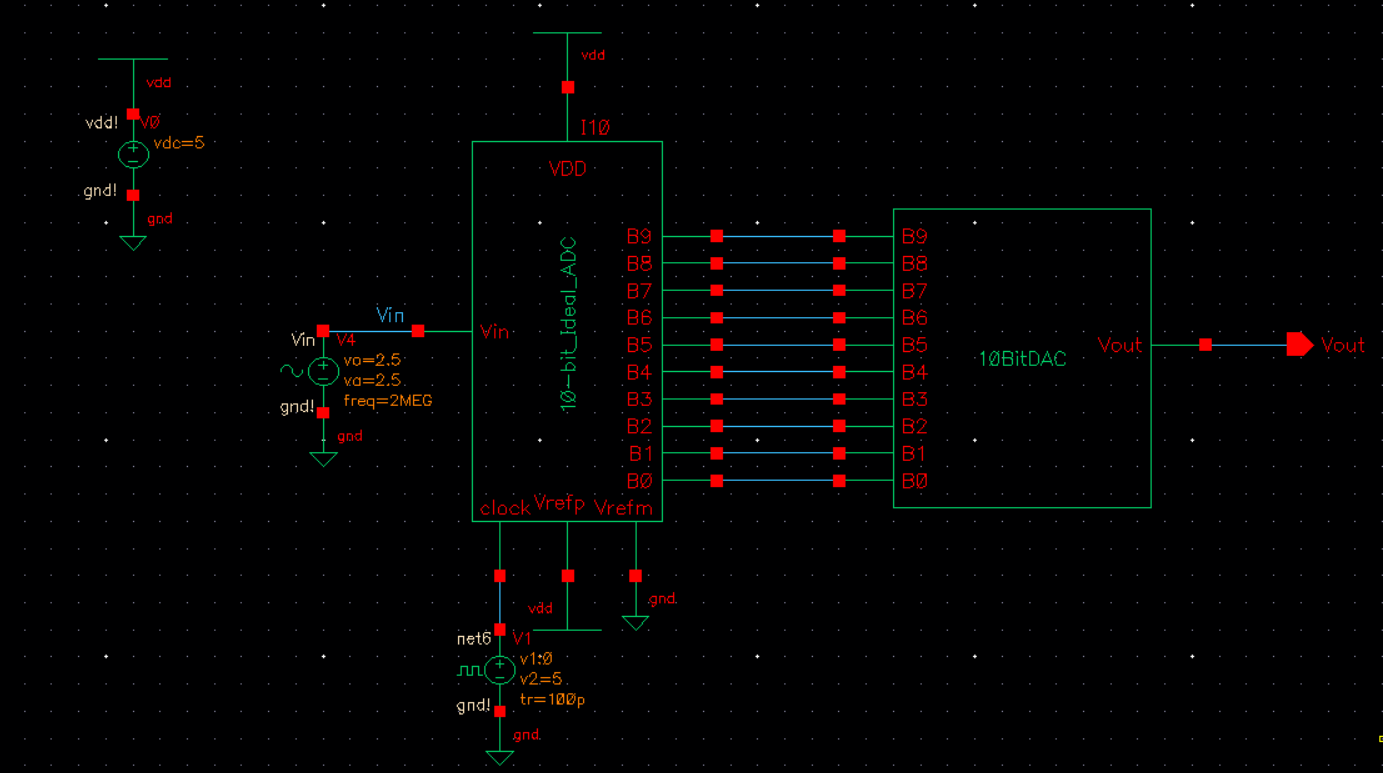
I will now load the sim_Ideal_ADC_DAC schematic in Cadence.
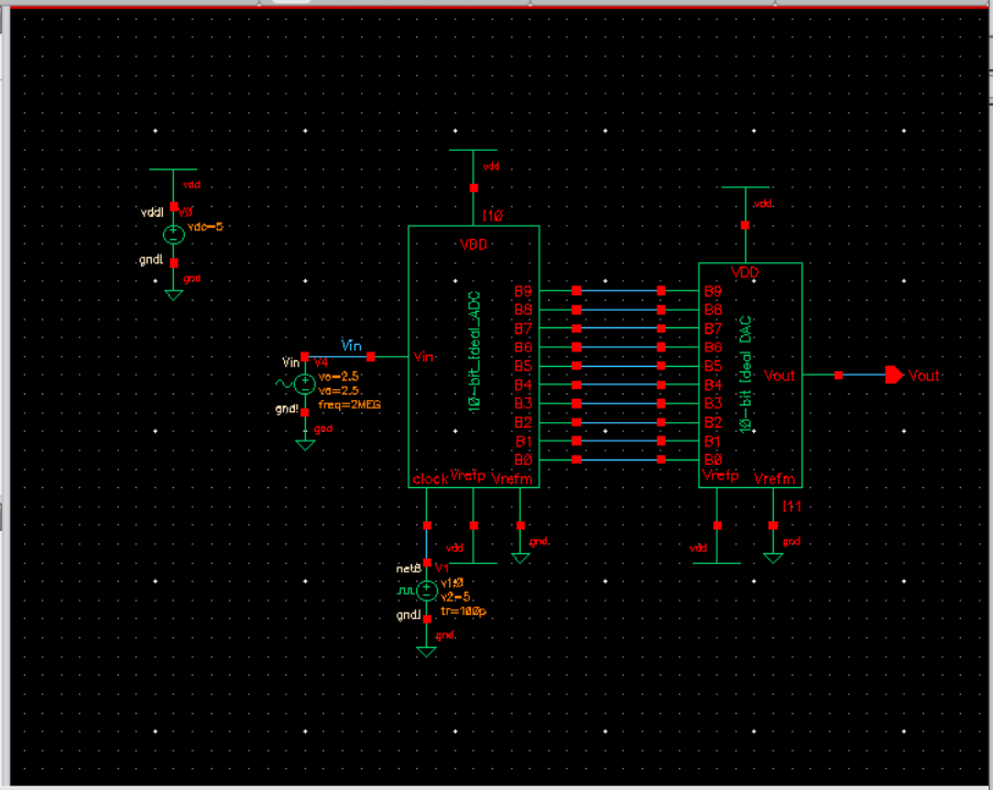
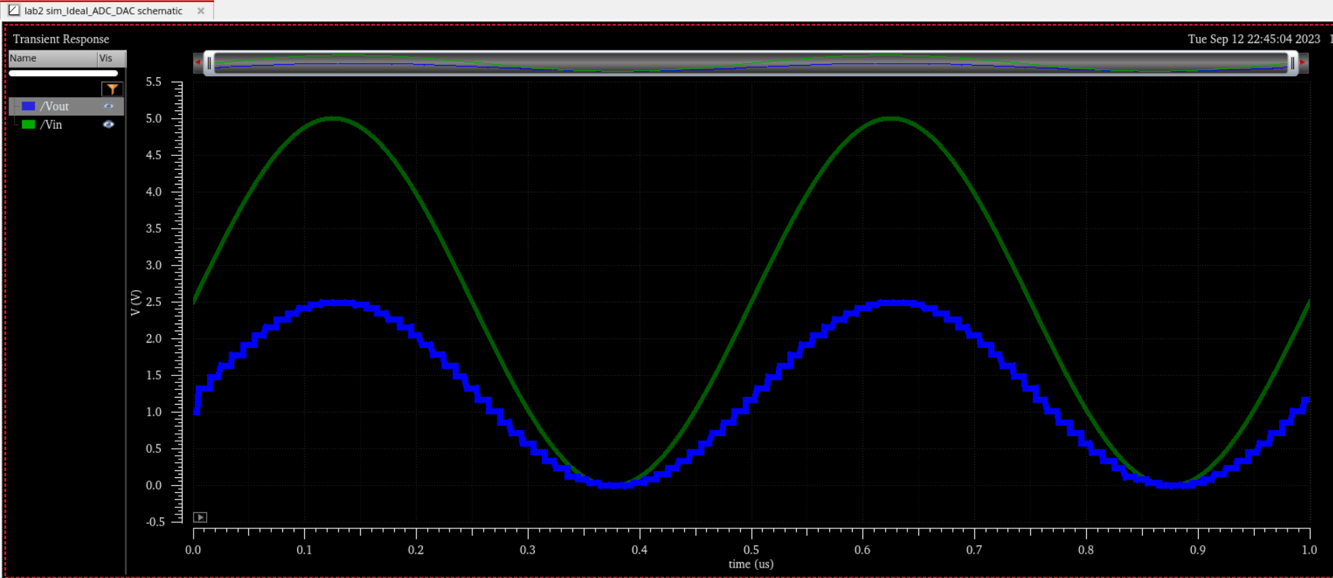
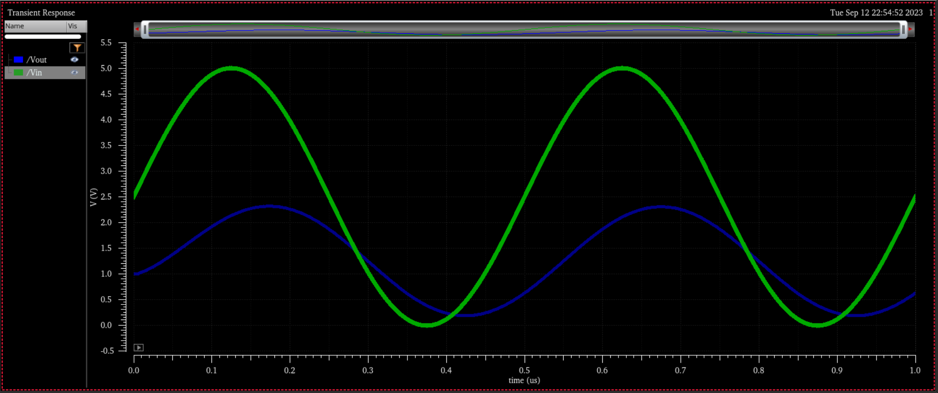
Plot Vin and Vout of the schematic.
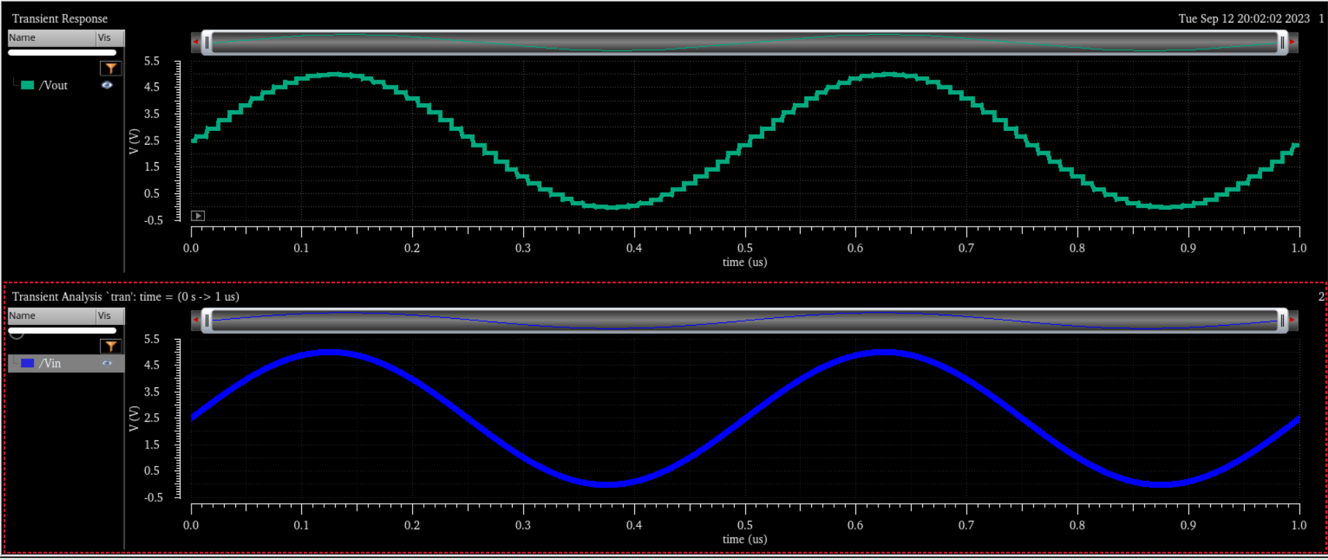
Looking
at the plot we can see the relationship between Vin, B[9:0], and Vout.
We can use the LSB (Least Significant Bit) formula to find the
relationship.
LSB will show the difference between the former and latter of the corresponding bit.
LSB=Vdd/2^n
LSB=5/2^10=4.88mv
4.88mv will be the output of the least significant bit.
For each bit, the output voltage will be halved. So at the highest bit (B9) 5V would halved which equals 2.5V.
Hence Vdd/2^n where n is the number of bits.
N=1 Vdd=5 5/2^1=2.5V
In the case of 10 bit, the last bit is B0 which would be the least significant bit
N=10 Vdd=5 5/2^10=4.88mv
Lab:
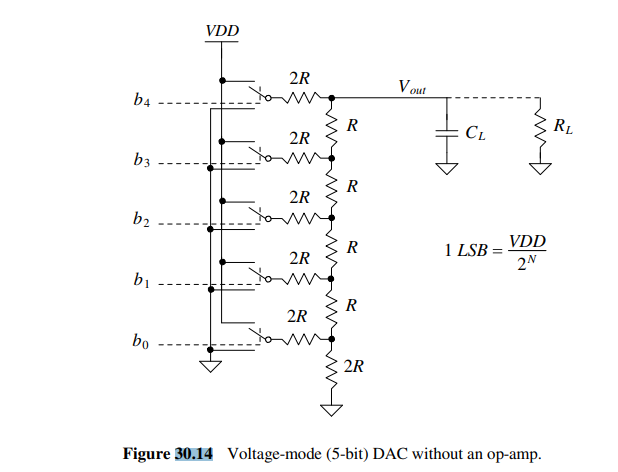
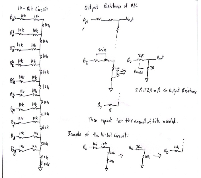
In this lab, I'll be using n-well resistors to implement a 10-bit DAC based on Figure 30.14 in the CMOS book.
First I will be designing a 2/3 voltage divider, which will represent a single bit of data.
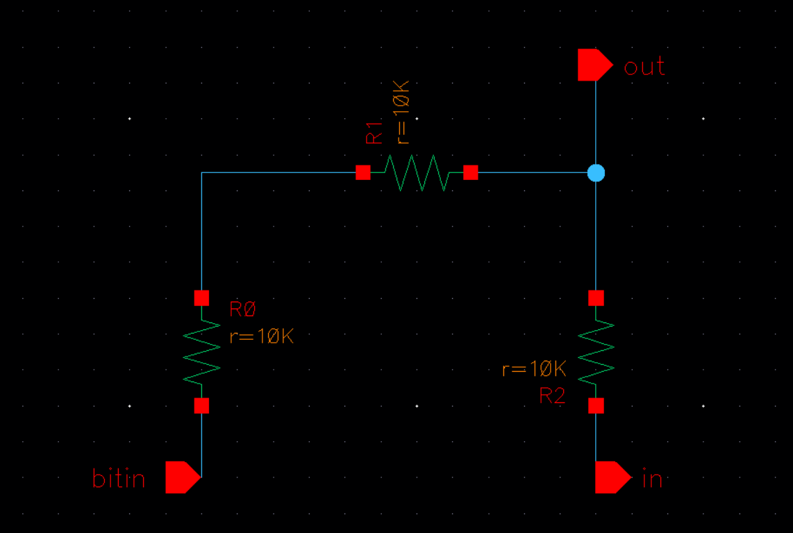
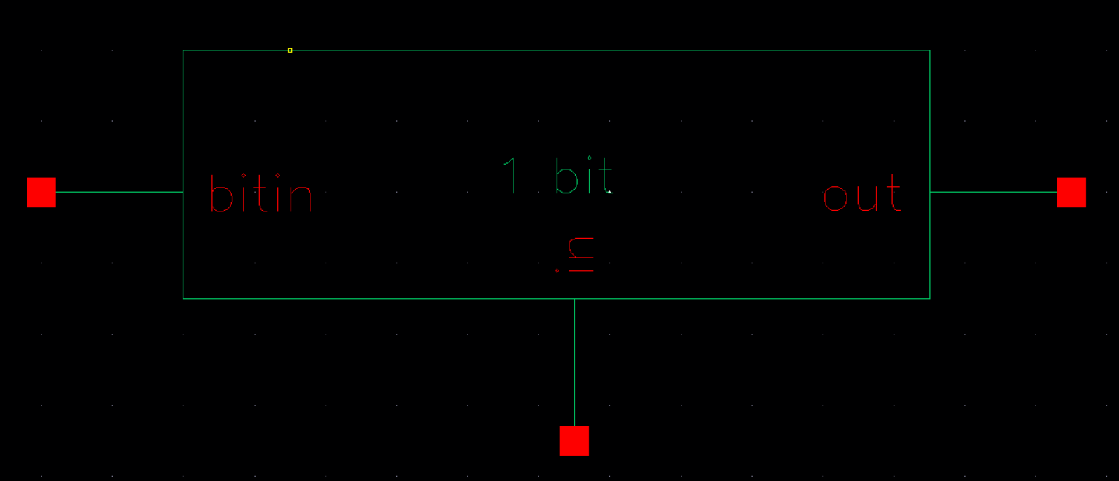
Then I will create a symbol that will represent the 2/3 voltage divider.
Using the 2/3 voltage divider symbol, I will make a schematic that will have 10 bits.
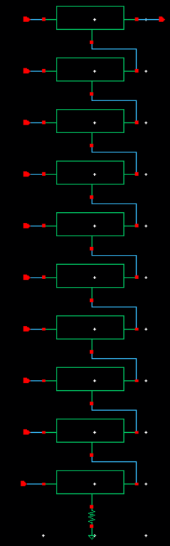
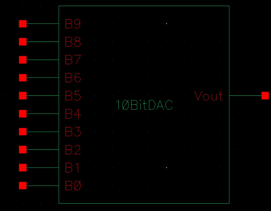
Using the schemtic, I can make a symbol that will represent the 10 bits into a single component.
Now I will be calculating the output resistance.
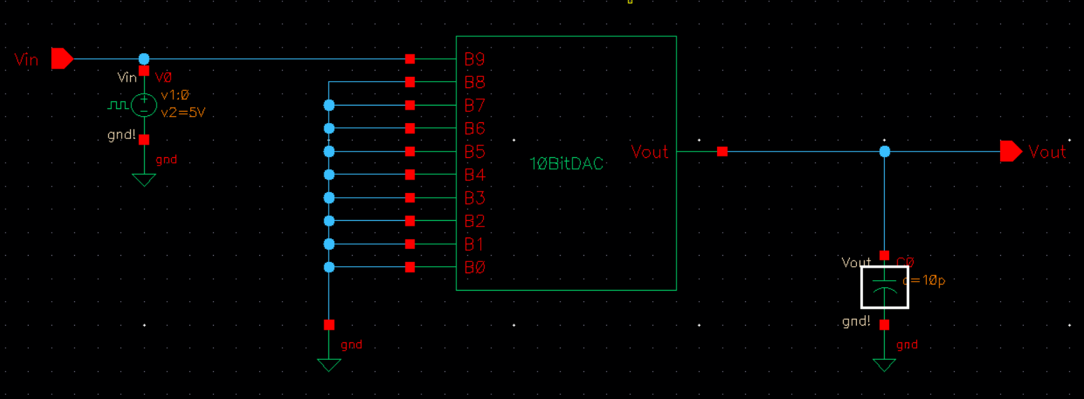
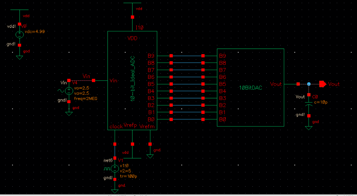
Now we test the 10-bit DAC to a load of 10pF, and grounding all inputs except B9.
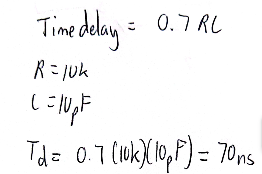
Calculations for time delay:
Plot of Vin/Vout:
Now I turn the schematic into a symbol and verify it works by inserting the 10-Bit DAC into the pre-lab schematic.
Plot of Vin/Vout:
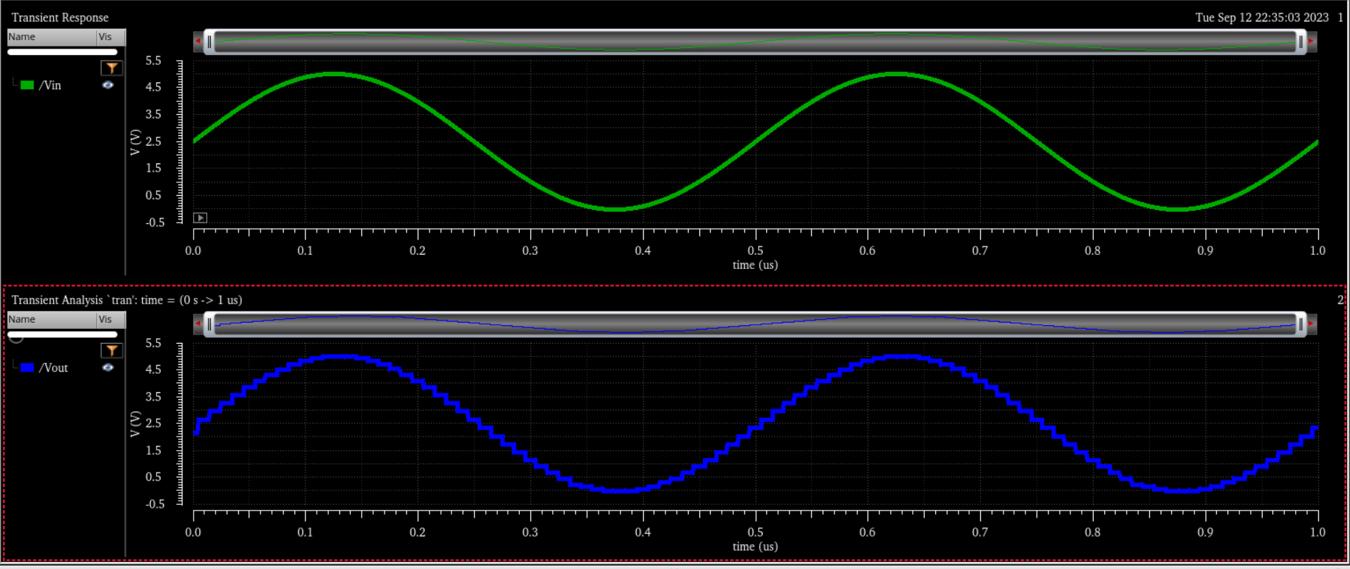
The plot above verfies that the new 10-Bit DAC symbol works due to the series of steps following the input voltage.
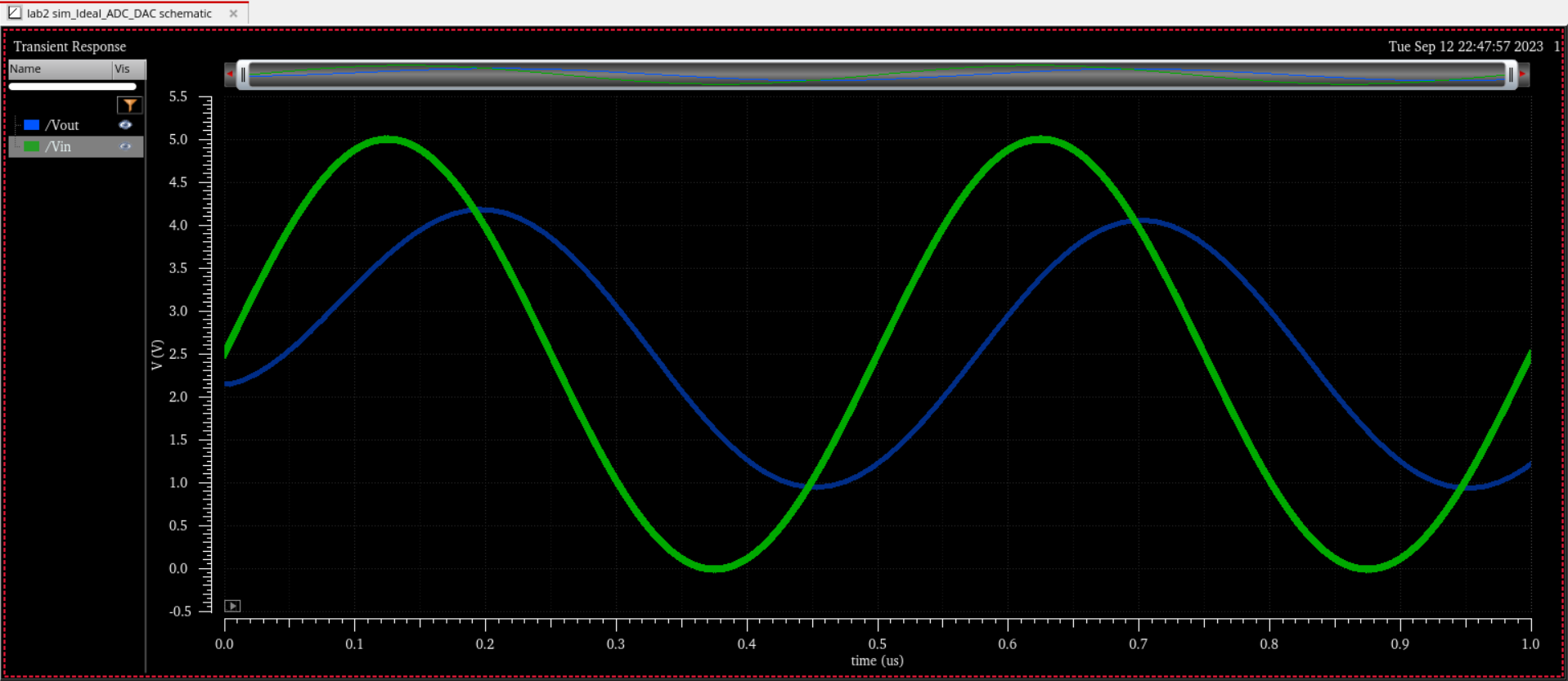
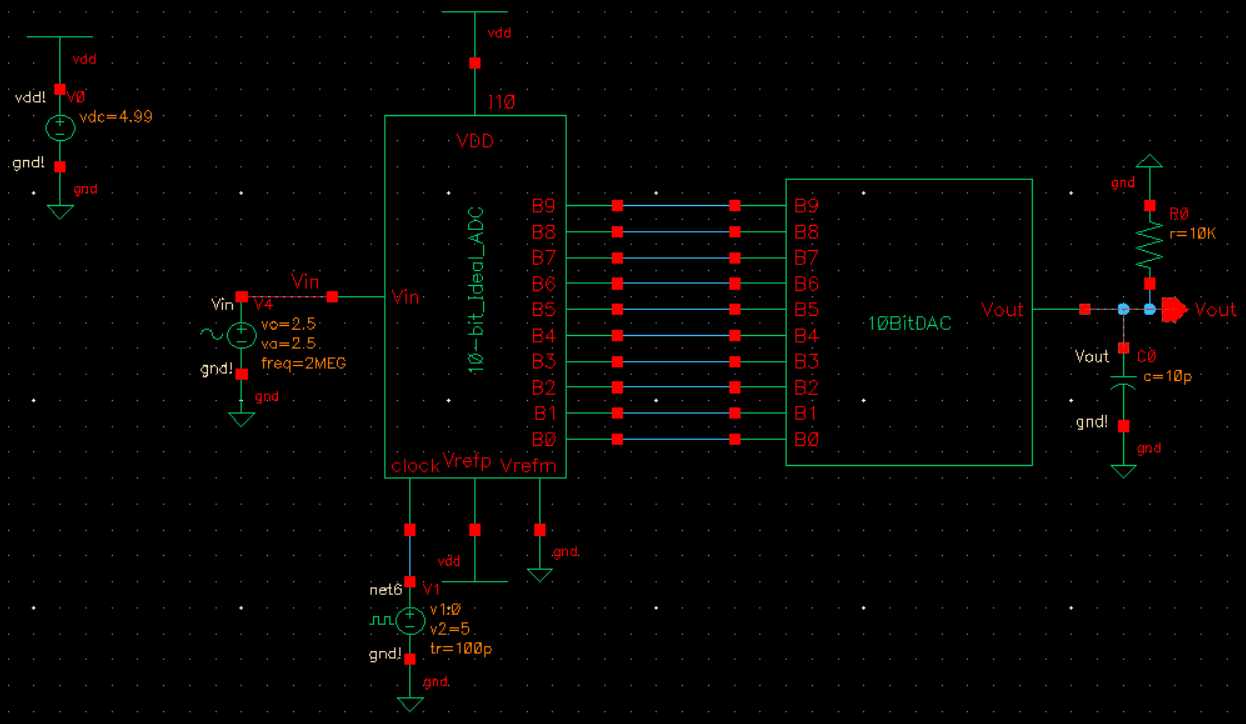
Now I will test the DAC when it drives a 10k load.
Withe the output resistance of 10k, the load will act as a voltage dividing which would then half the output voltage.
The plot verifies this.
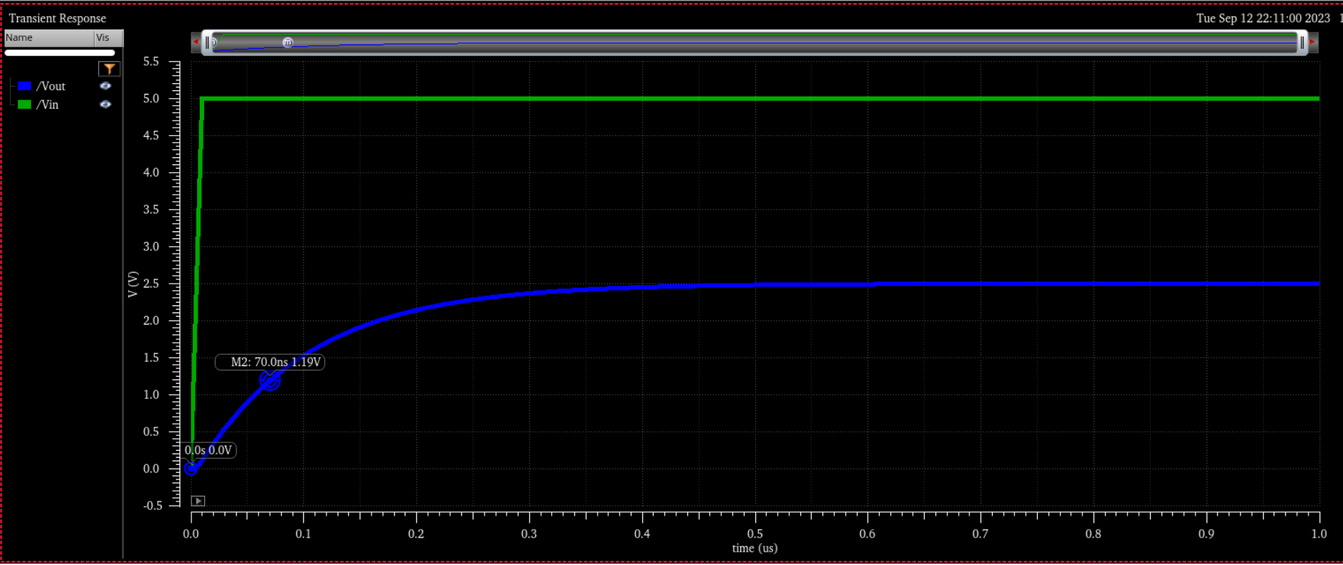
Now I will test the schematic with a 10pF load.
We should see a delay in the plot.
Now I will test the schematic with a resistive and capacitive load.
We should see the voltage halved with a delay.
In
a real circuit the switches seen above are implemented with
transistors. So if the resistance of the switch aren't smaller compared
to R,
resistance would be added in series to each of the voltage
dividers. Higher impedances would cause a higher output resistance
which would then cause
the voltage drop across the resistance would be also higher.
Return to EE421 Labs