Lab 7 - ECE 421L
Authored by Josue Magana Quezada
Email: maganaqu@unlv.nevada.edu
11/08/2023

Prelab
For this prelab we will folllow the steps from Tutiorial 5
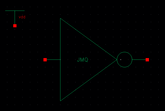
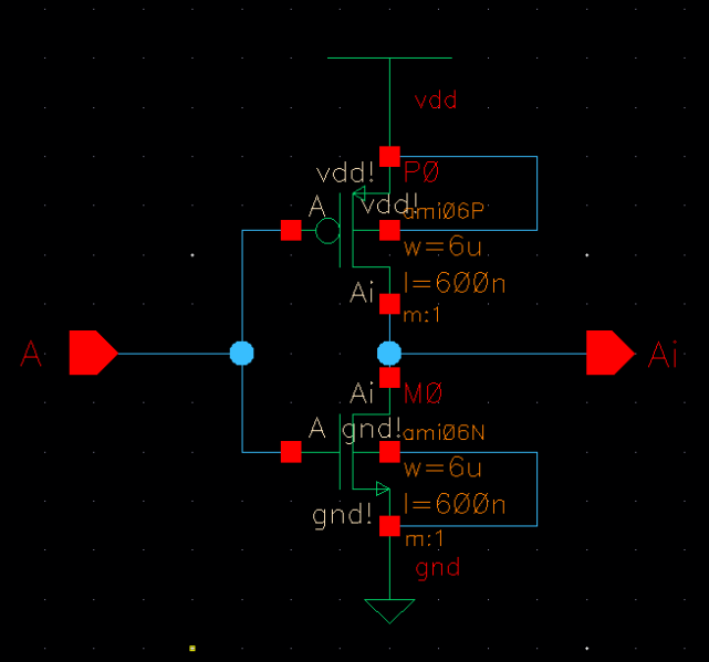
First we have the schematic for the ring_osc
and then the same inverter with multiple ones at the same time connected

Labeling process...
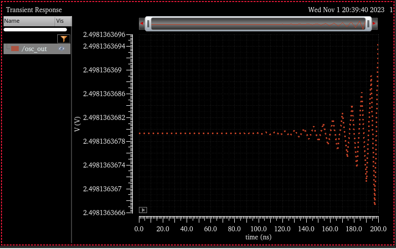
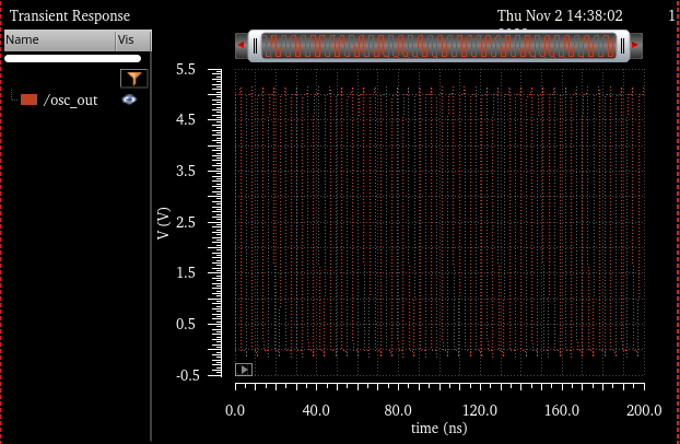
Result from .tran that is aroud 2.5V
The coming result is for setting up an initial condition where we set the Node Voltage to 0
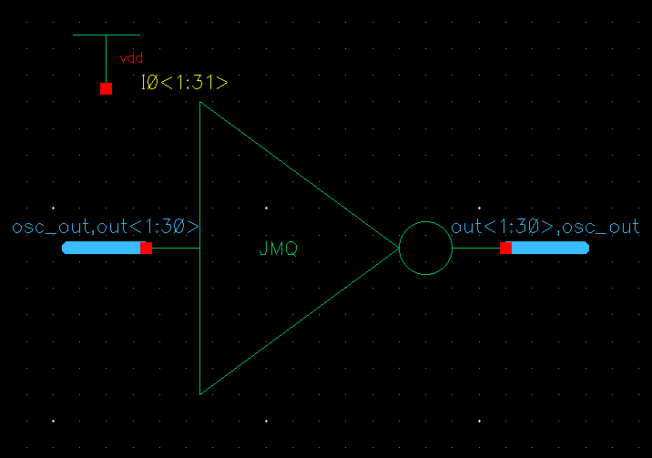
We create a bus wire on the input and output of the inverter. In addition, in order to avoid
having so many inverters connected in series, another solution is creating an instance name.
For example, in this case we have it as I0<1:31>
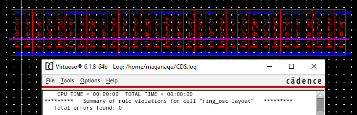
Now a layout for the ring oscillator with DRC clean
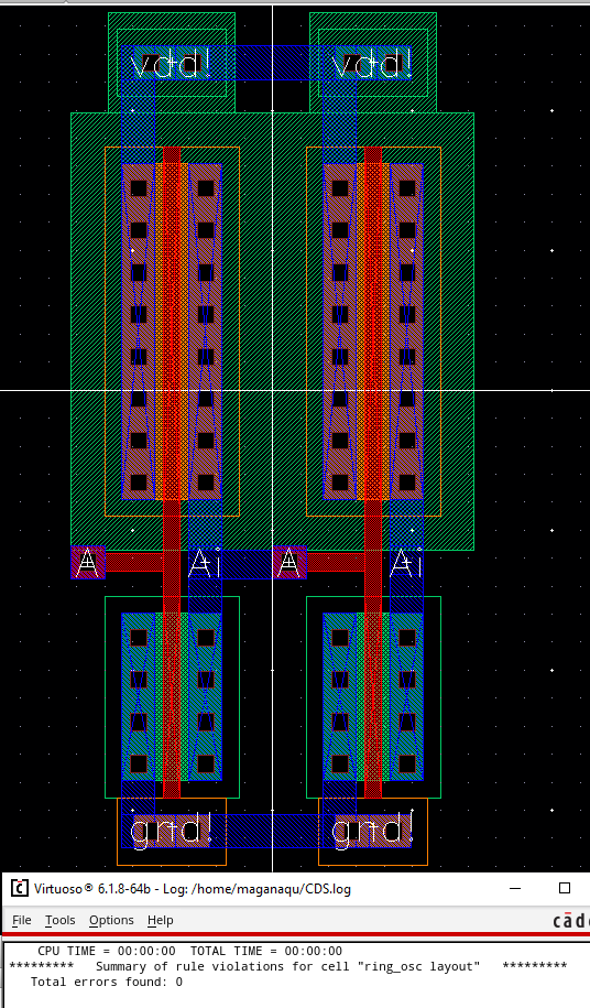
As well as the full layout with DRC clean
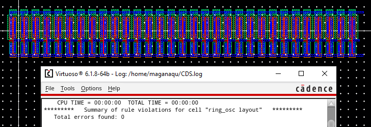
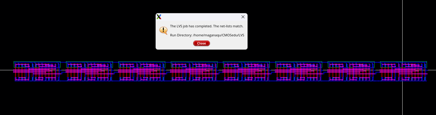
And the extracted version wtih LVS, however this version failed since we still have to do another step.
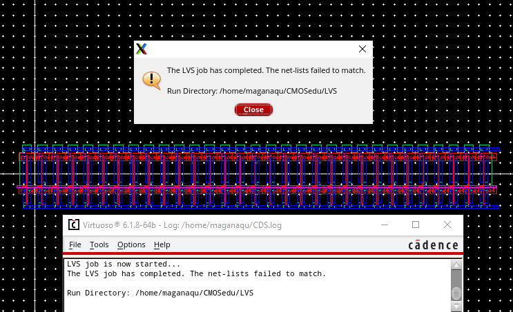
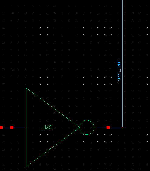
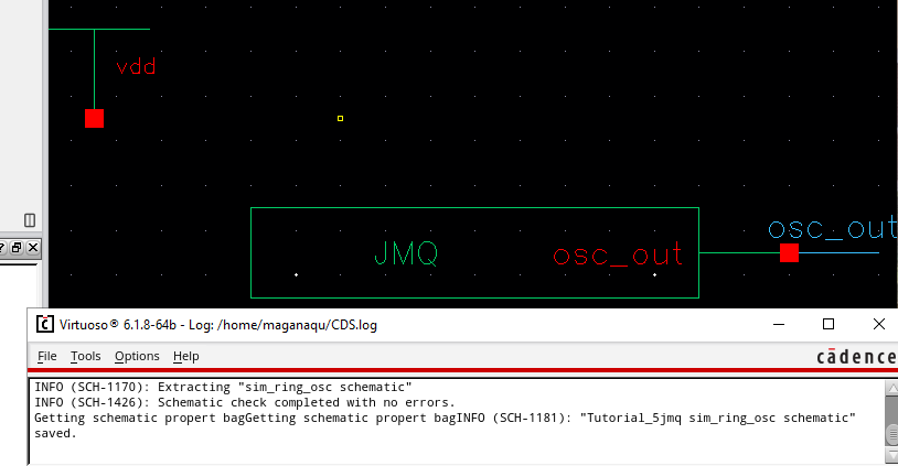
So to fix that issue we recall a pin osc_out in the schematic
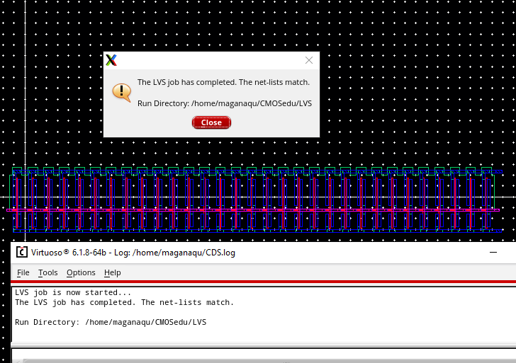
And now, it works!!!
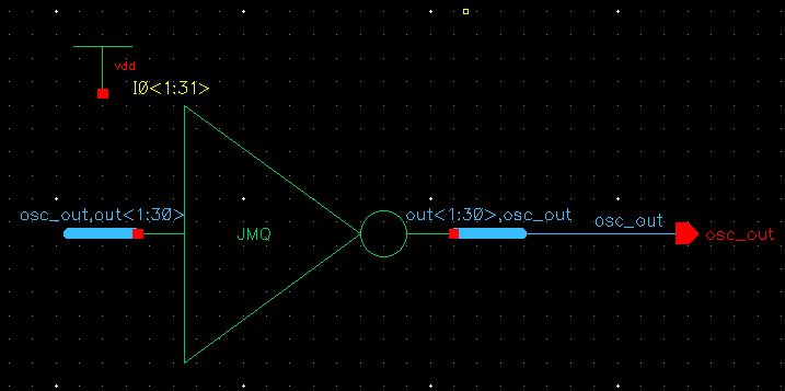
So now, we will create a symbol and a schematic
And we are ready to simulate our new schematic
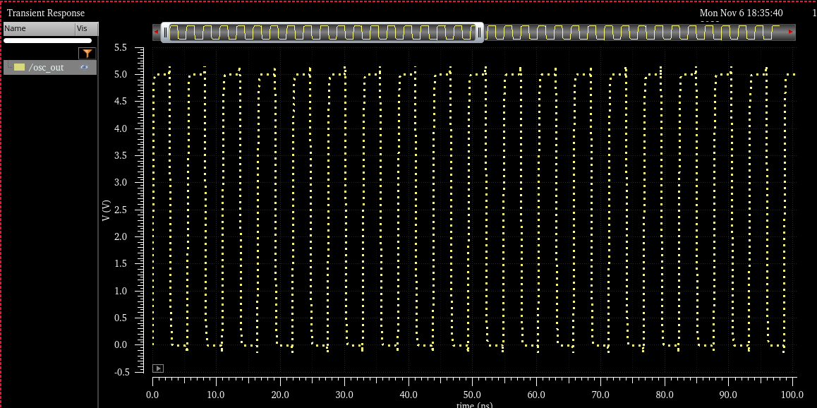
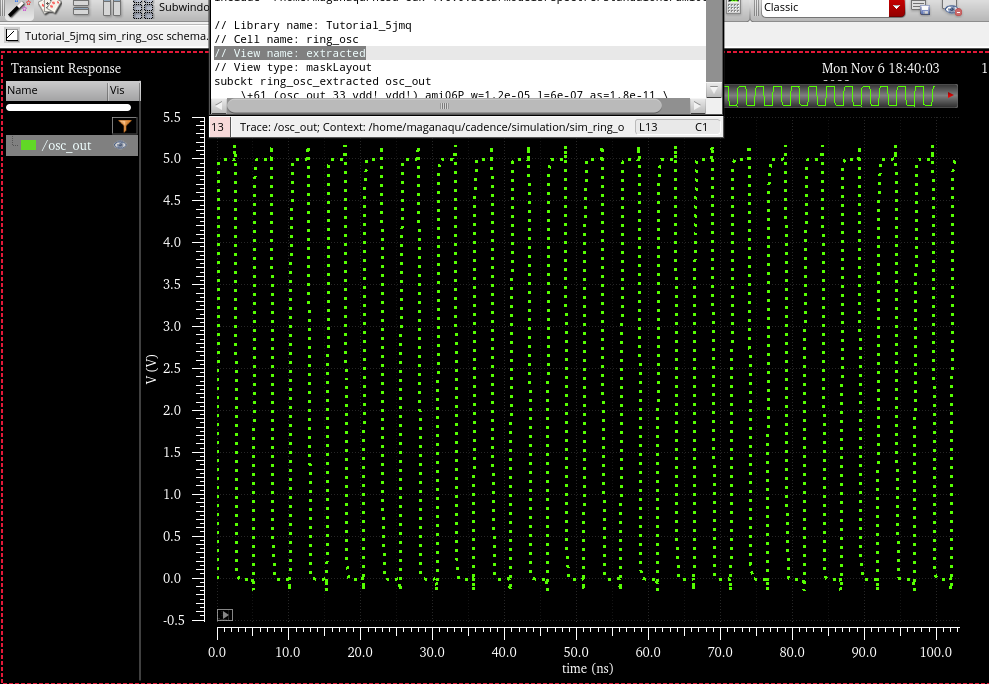
Finally, we can also ran the extracted view. As we can see below, the picture shows is running with the extracted.
Lab Work
For the coming lab we will work with 6u/600n PMOS & NMOS inverters
Here symbol of the inverter
A cell of the inverter 4 bit
And symbol of it
Now, lets use that symbol to create or schematic
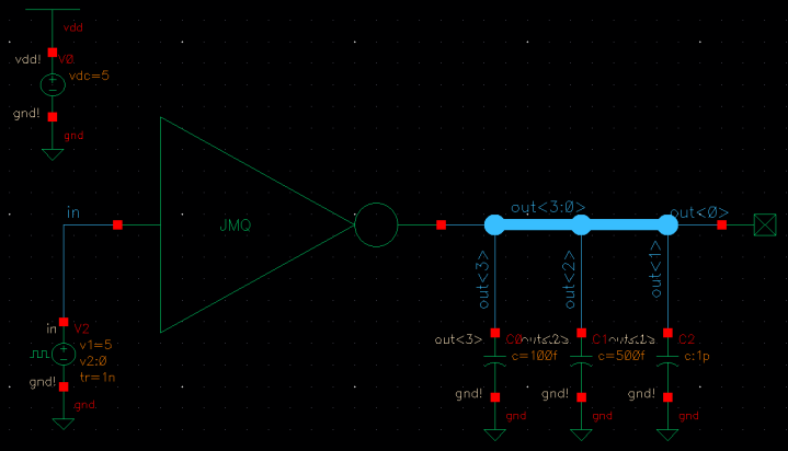
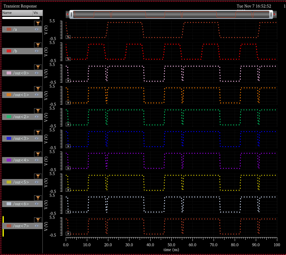
And here we have the simulation of the 4bit inverter
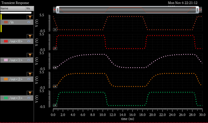
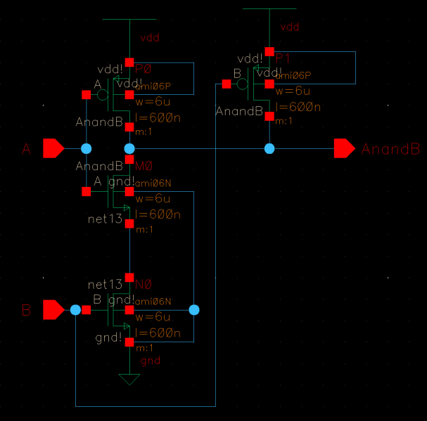
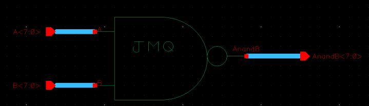
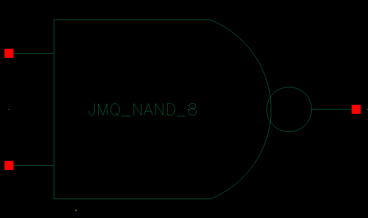
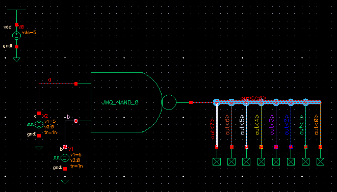
NAND gate
Schematic
 | 8-bit schematic
 | 
8 bit symbol |
 |  | |
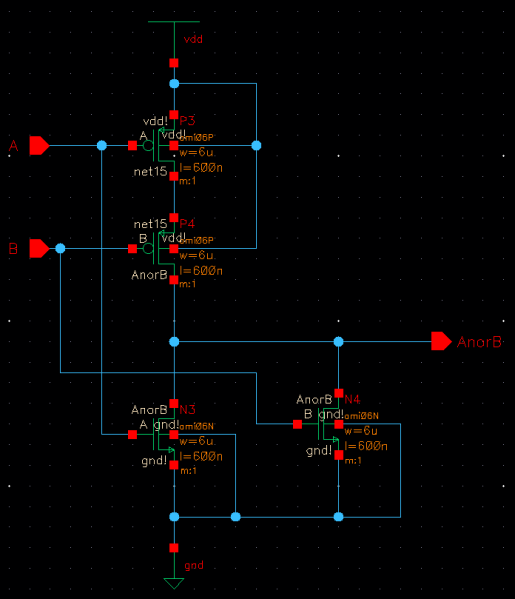
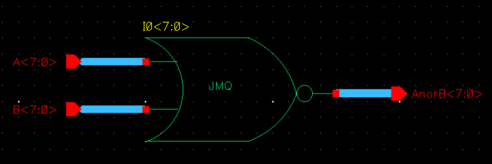
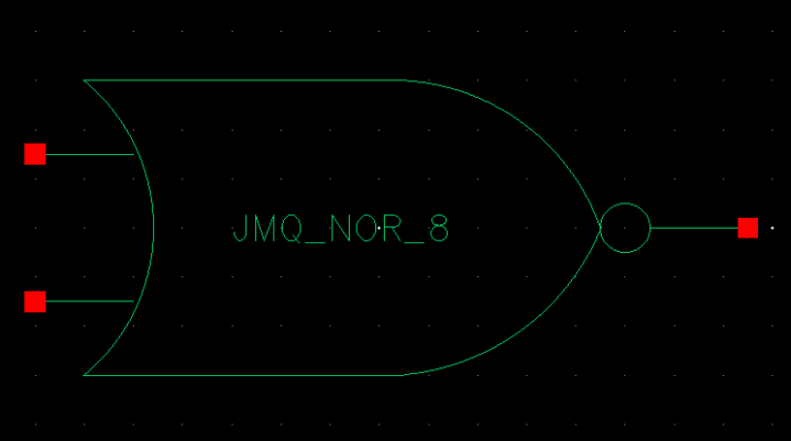
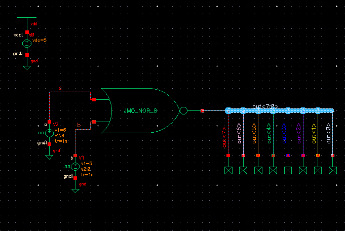
NOR gate
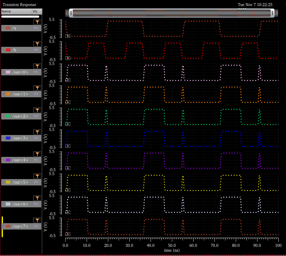
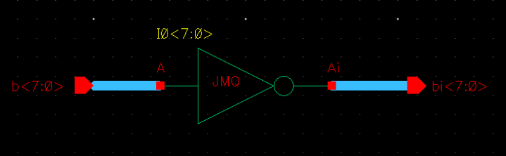
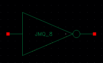
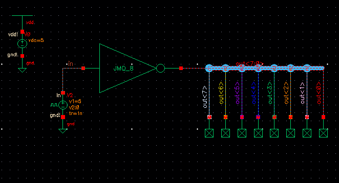
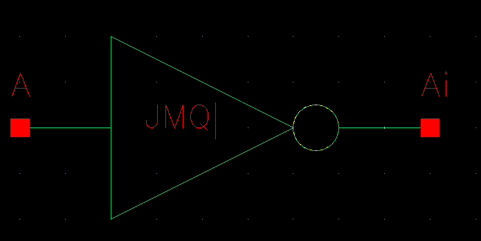
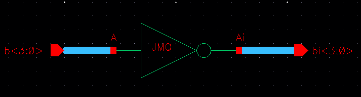
NOT gate, using the 4-bit schematic. but now adapting to 8-bit
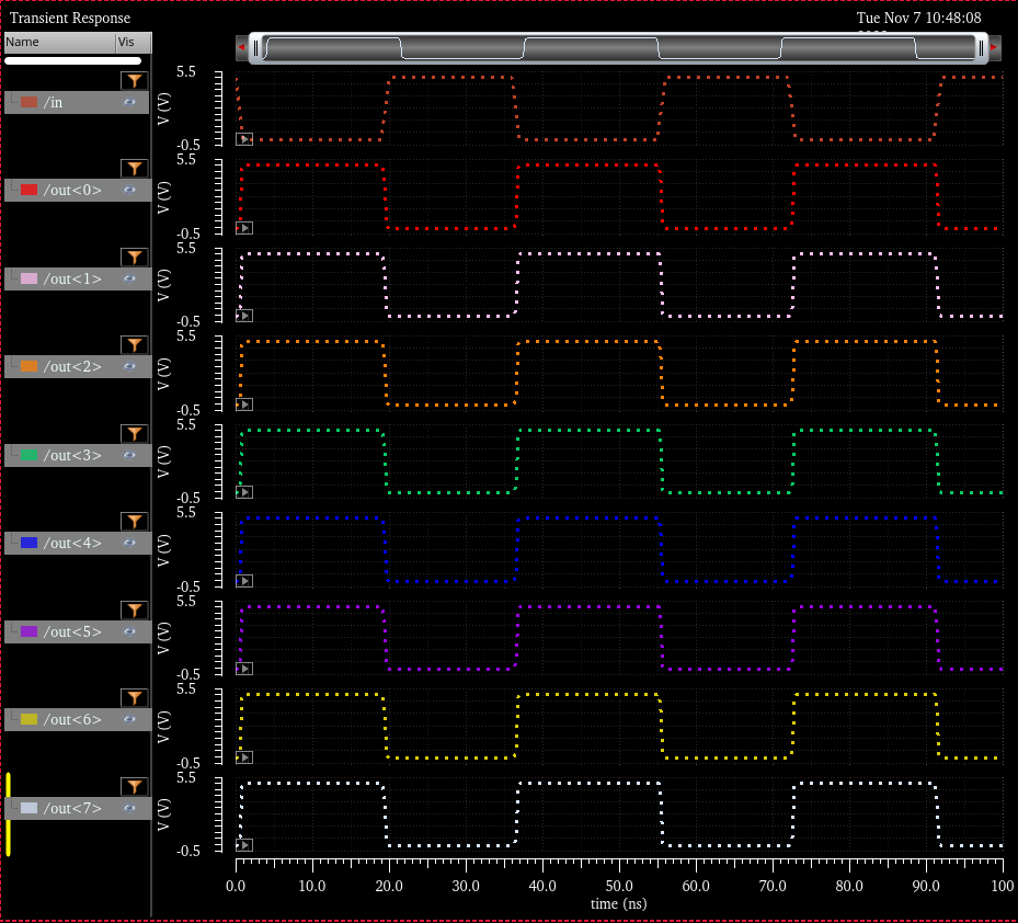
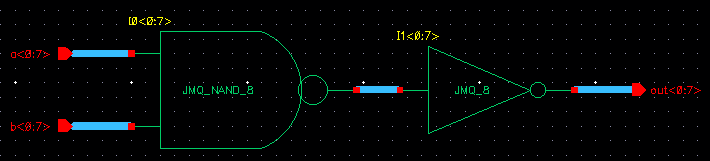
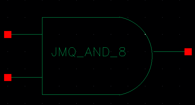
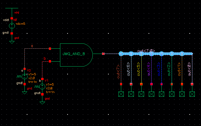
AND gate, for this schematic we have the NAND and NOT together.
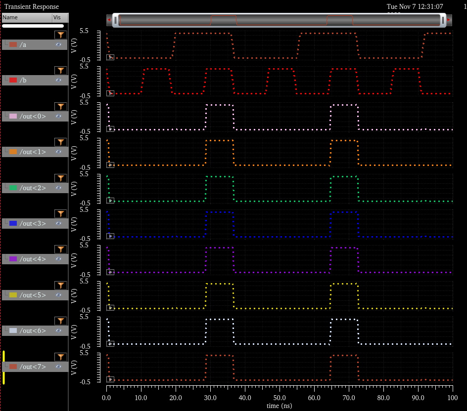
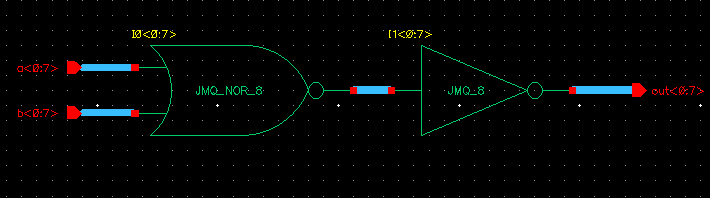
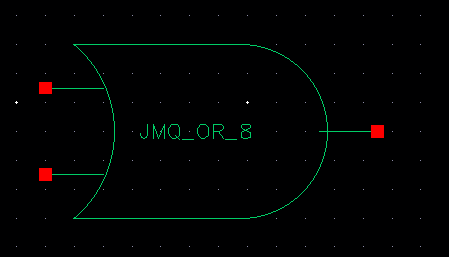
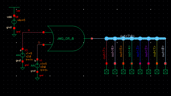
OR gate, for this schematic we have the NOT and NOR together.
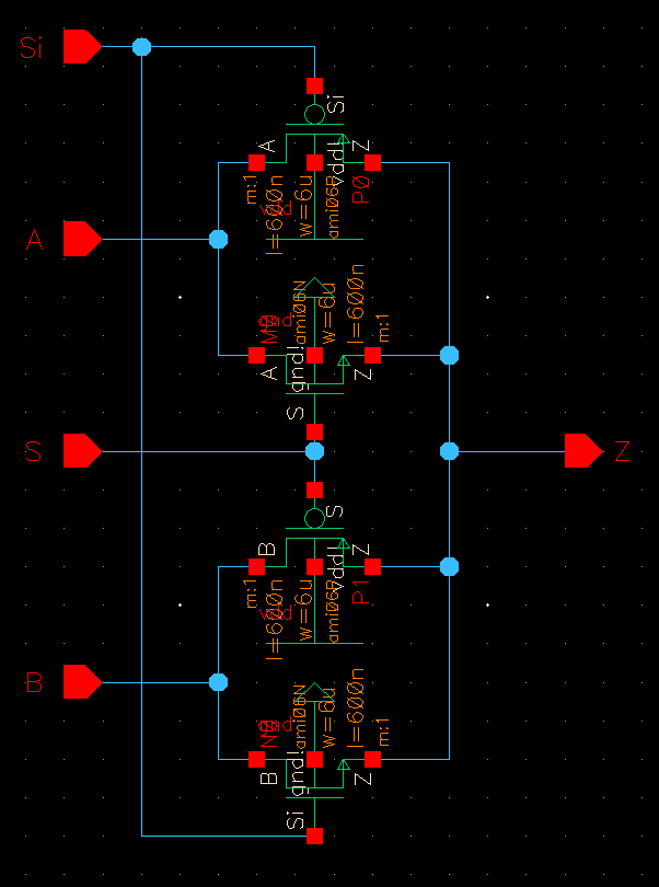
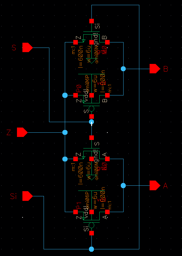
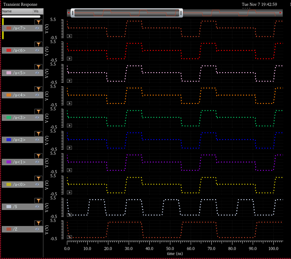
Now, lets have the MUX with the schematic
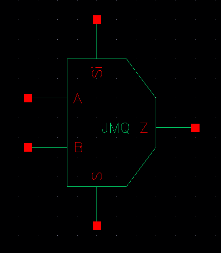
Symbol of the MUX
Schematic for the 8-bit MUX
its symbol with the schematic
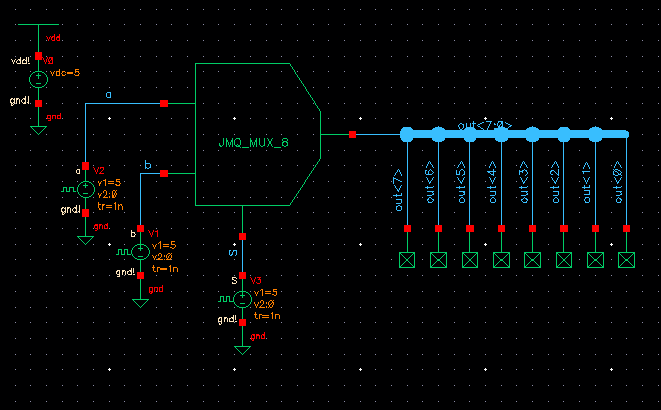
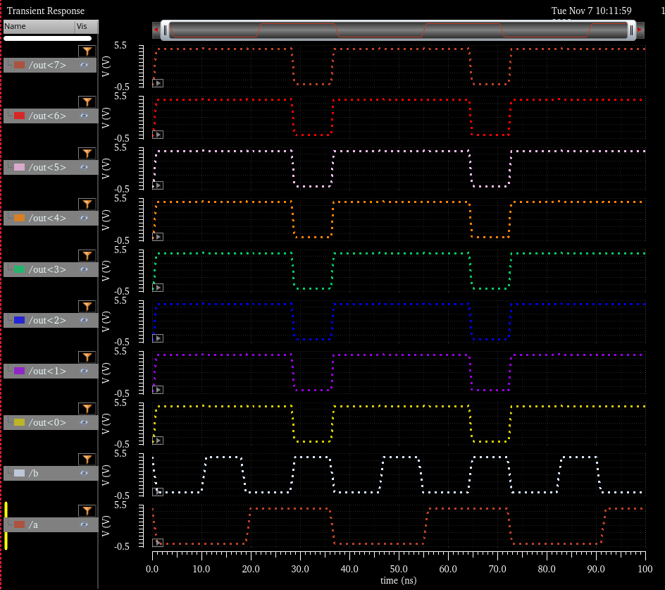
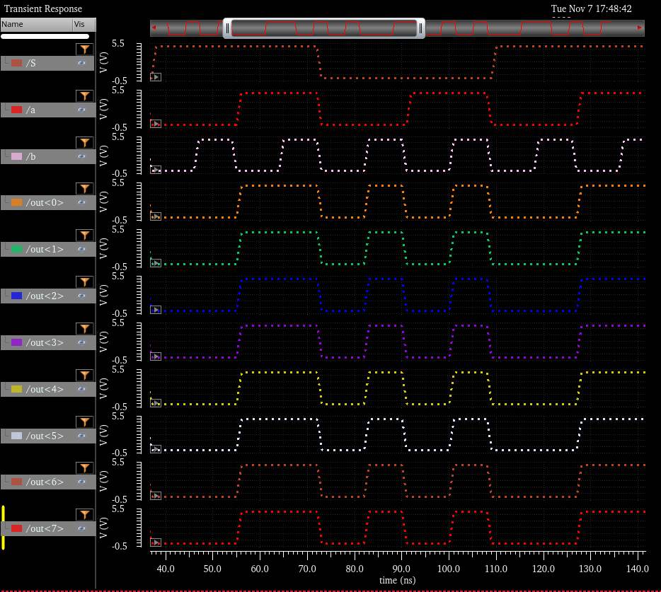
Simulation
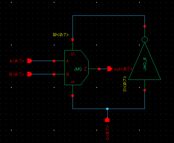
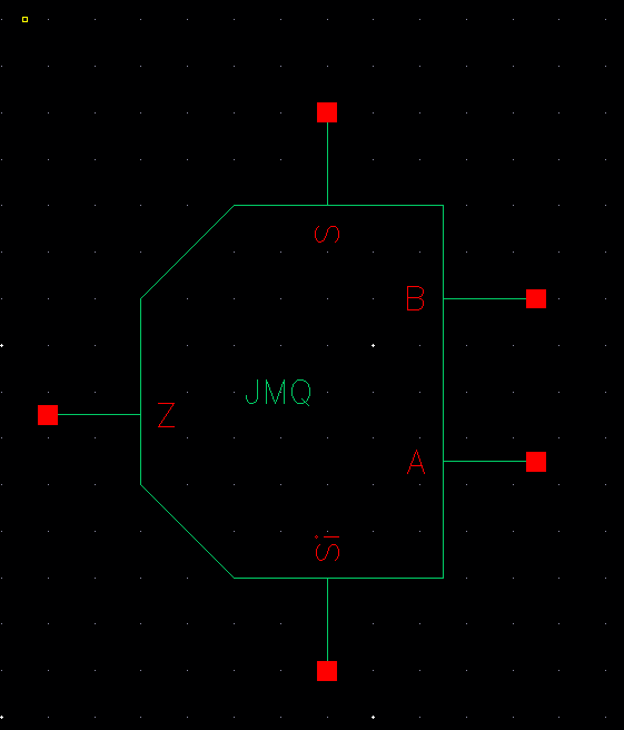
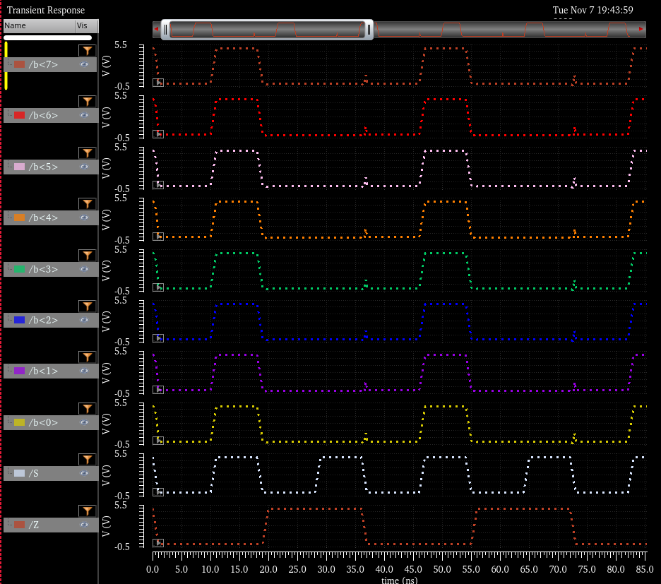
Now lets have the schematic for the DEMUX
SYMBOL
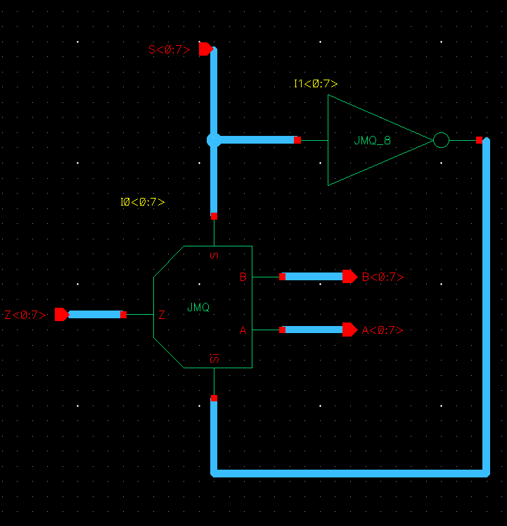
Schematic of the DEMUX but with 8-bit
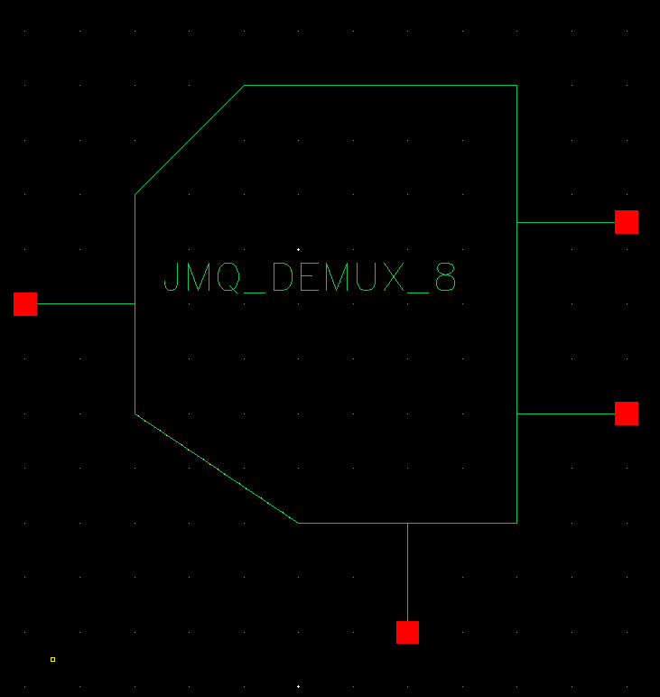
Symbol of the 8bit demux
Schematic
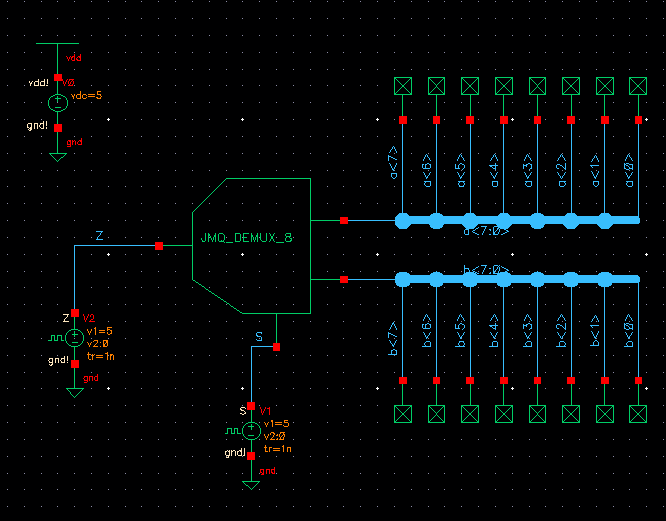
and sims
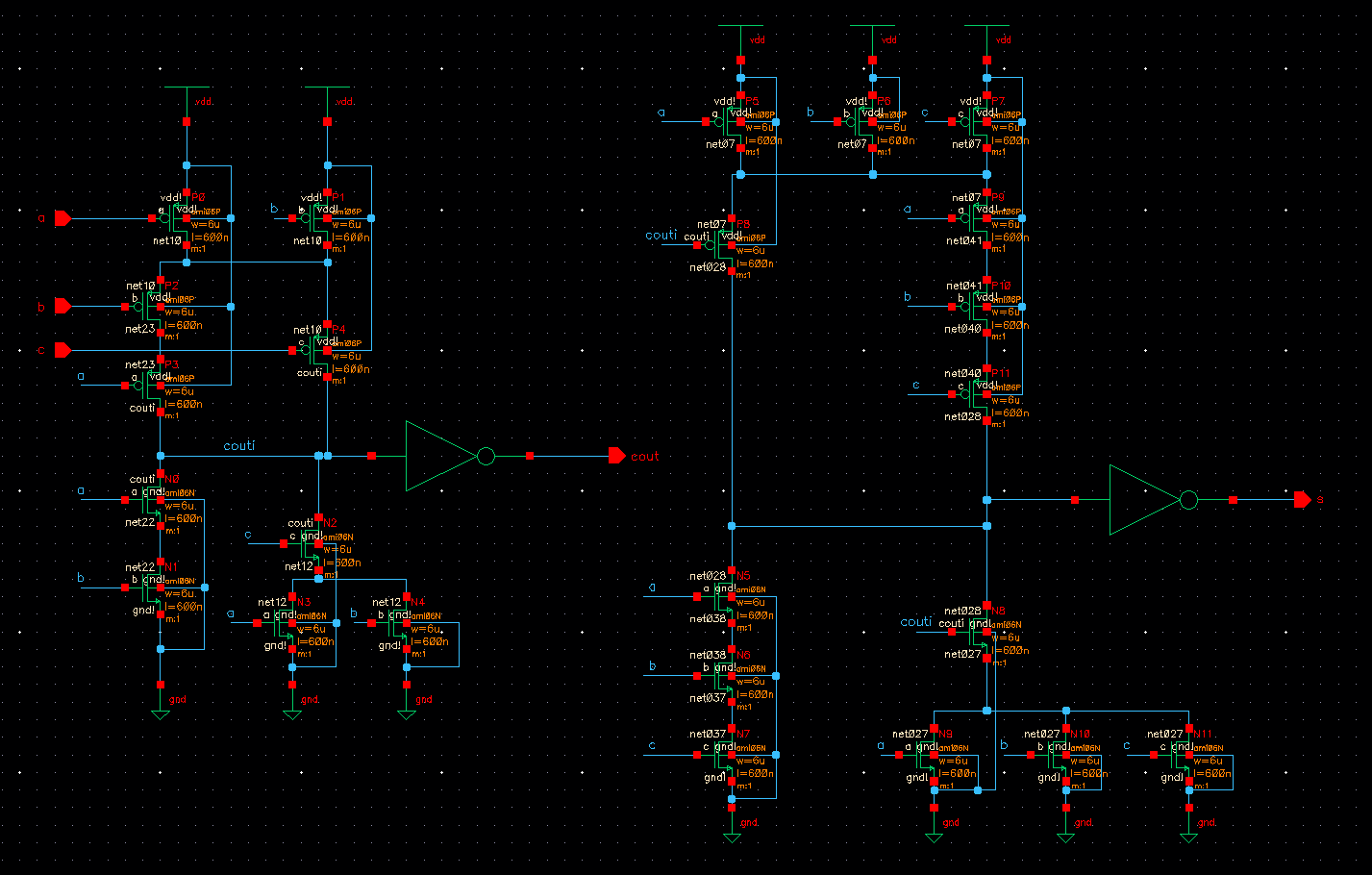
Now following figure 12.20 from CMOS book, we have this schematic
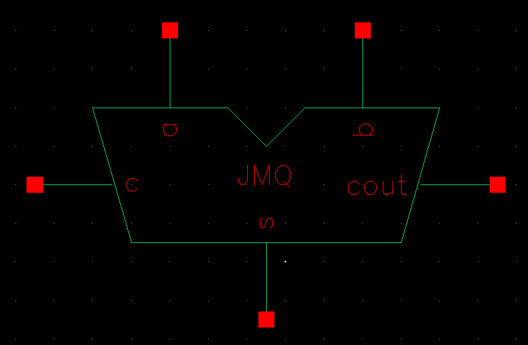
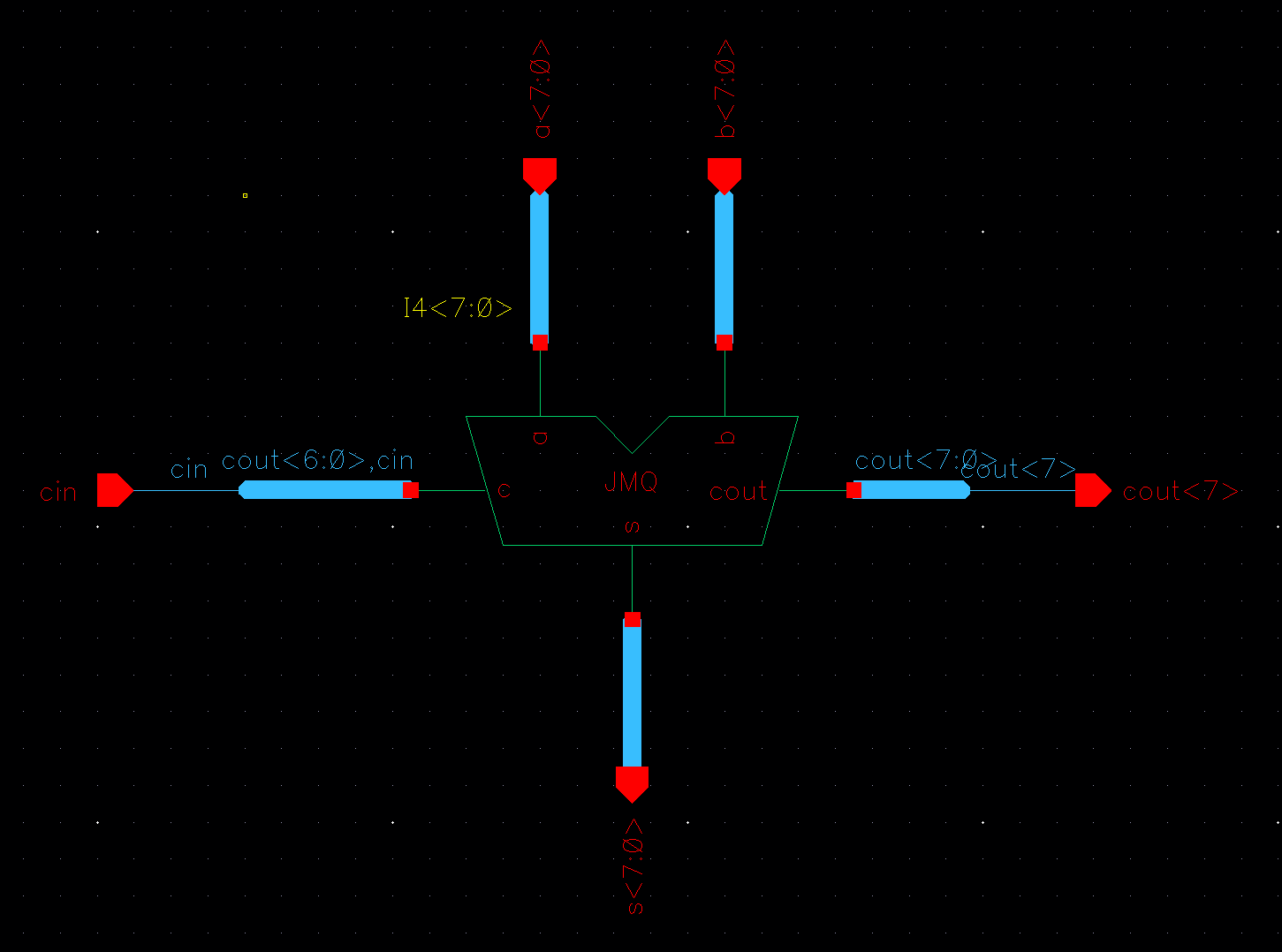
With that, we can create our fulladder symbol
adding 8-bit to the schematic
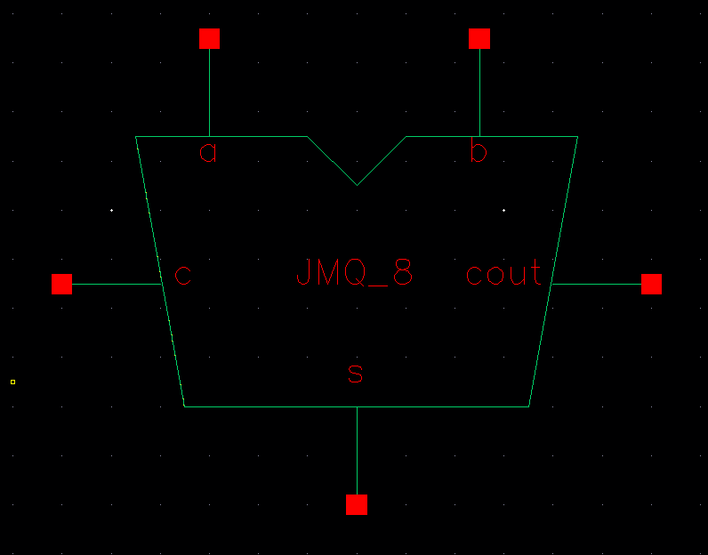
Creating a symbol of the fulladder with 8bit
Now, lets make the layout of the fulladder with DRC clean
Extracted view with LVS clean
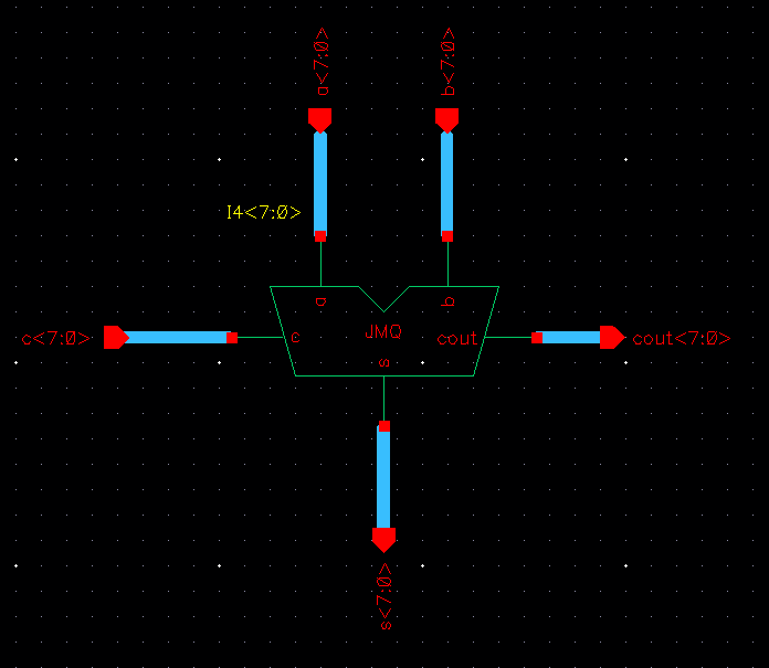
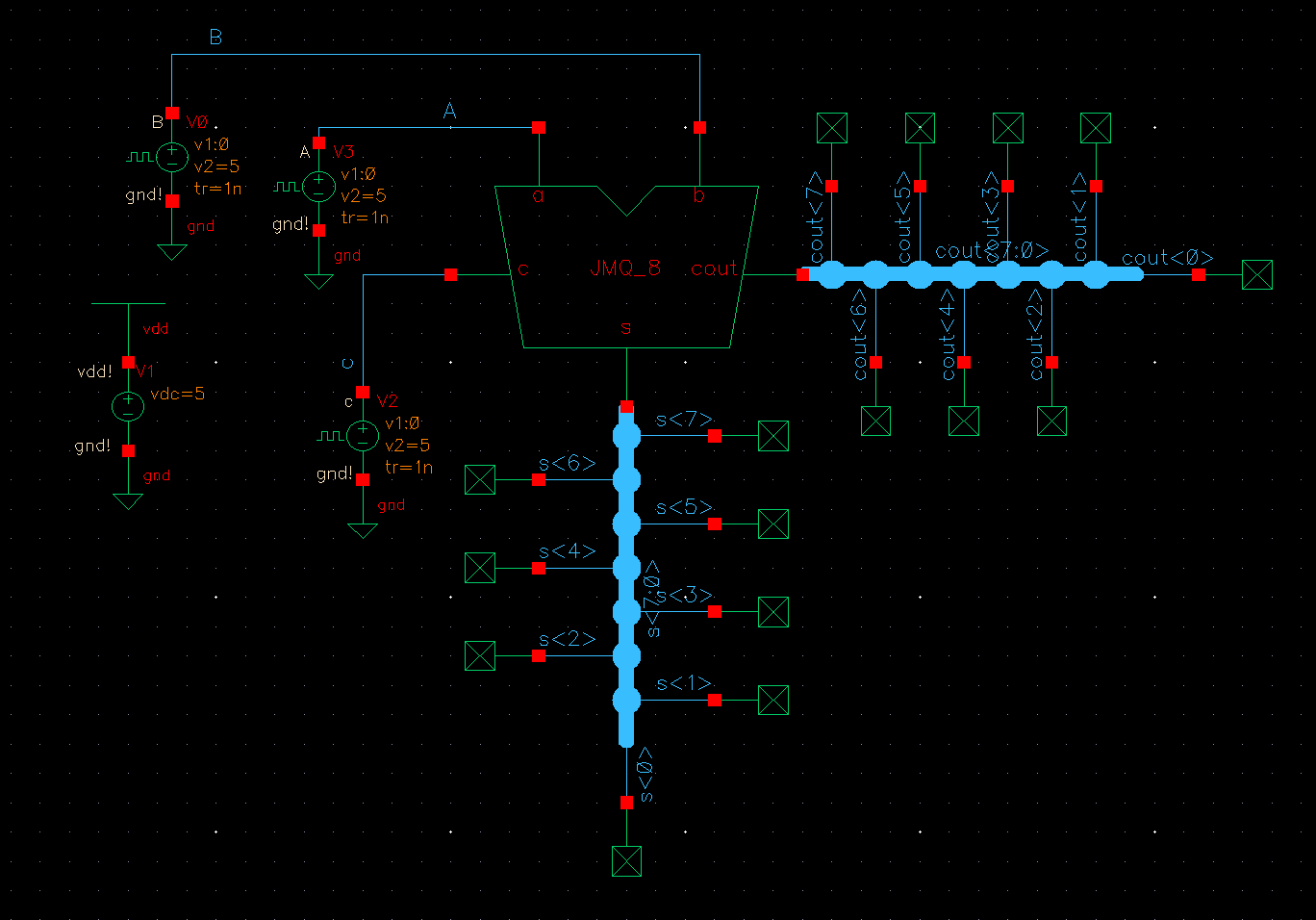
Creating our fulladder as an 8bit gate
Schematic of the fulladder 8bit
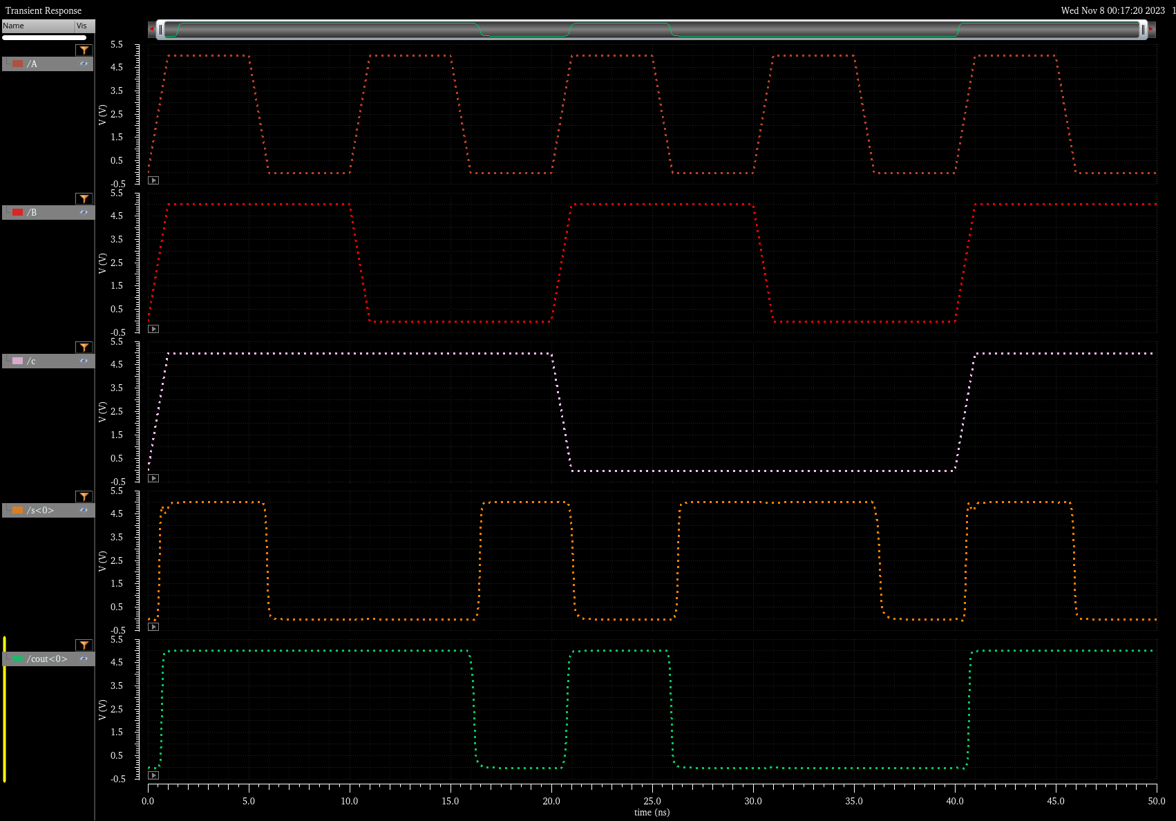
sims
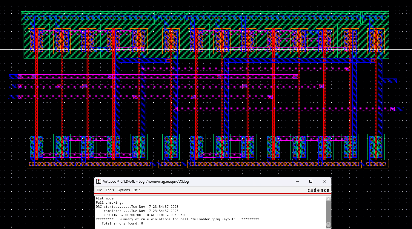
Layout with DRC clean
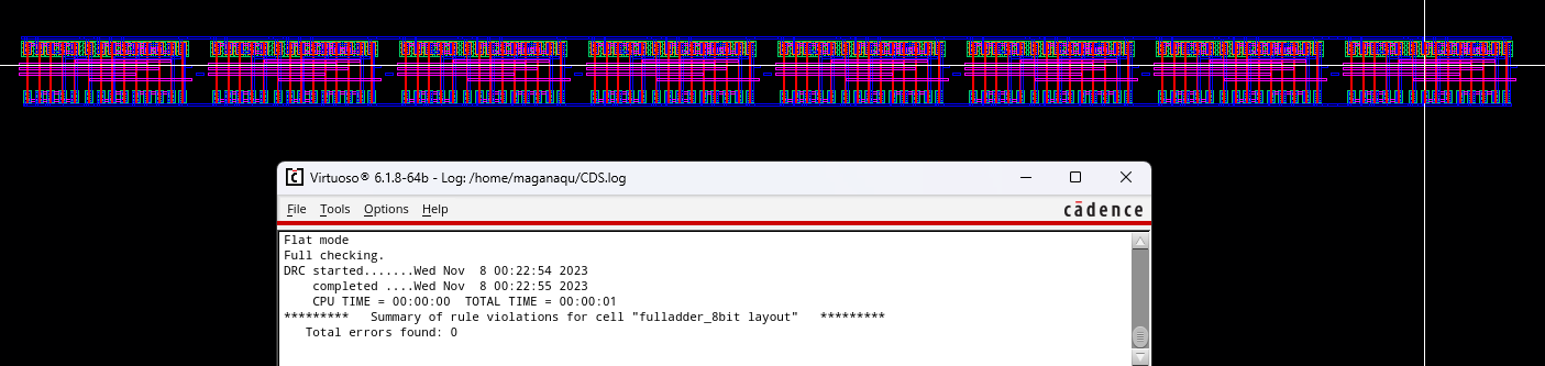
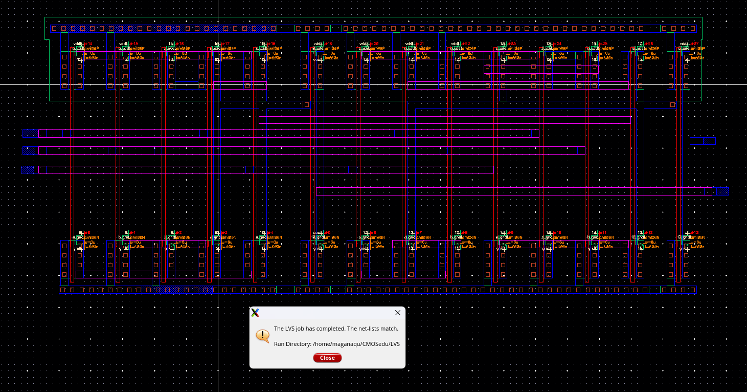
Finally extracted view with LVS clean
Back up
Return to EE 421L Labs