Lab 6 - ECE 421L
Authored by Josue Magana Quezada
Email: maganaqu@unlv.nevada.edu
10/27/2023

Prelab
For
this prelab, we have to follow Tutorial 4 which helps for design,
layout as well as simulate a NAND gate. Important thing is doing
verifications of the design such as DRC for layout and LVS for the
extracted.
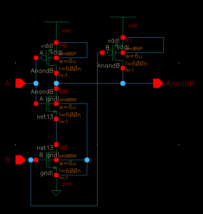
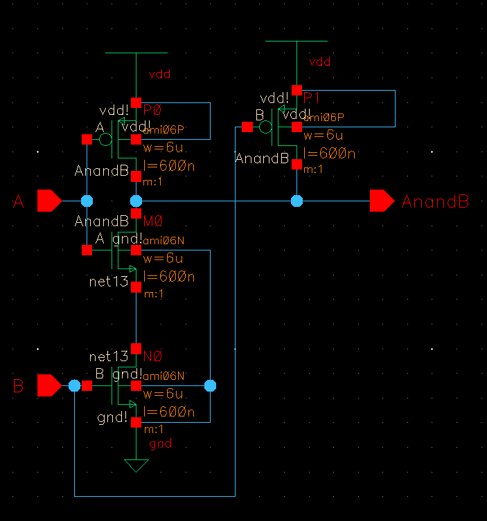
On this picture, we can see the schematic of the NAND gate
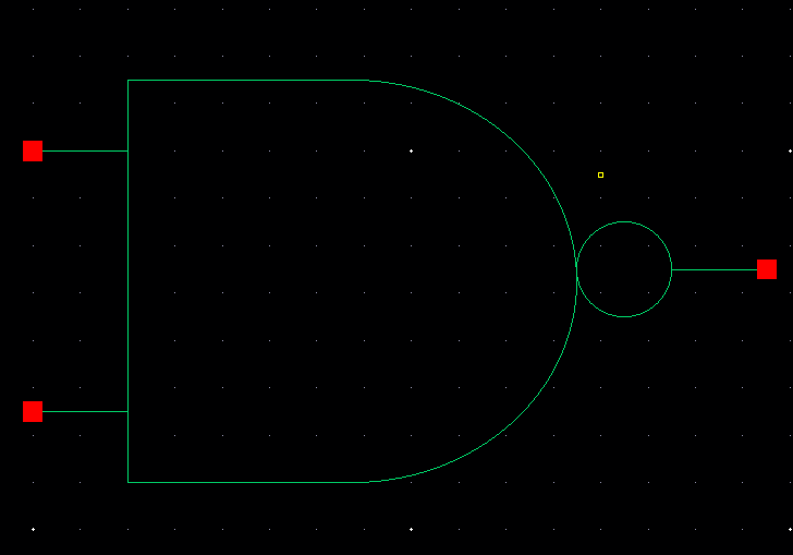
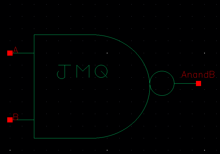
Symbol of the NAND gate
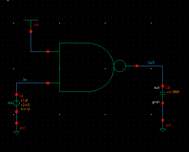
Here the circuit to test our symbol.
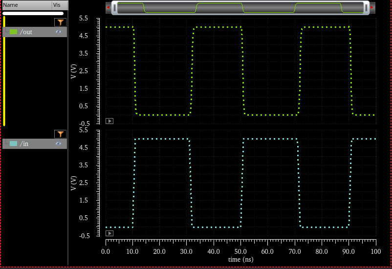
and the result of the spectre simulation. we can see that when IN is 0, OUT is the opposite
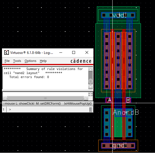
Now, in this picture we can see the layout of NAND gate, as wel as the DRC verification
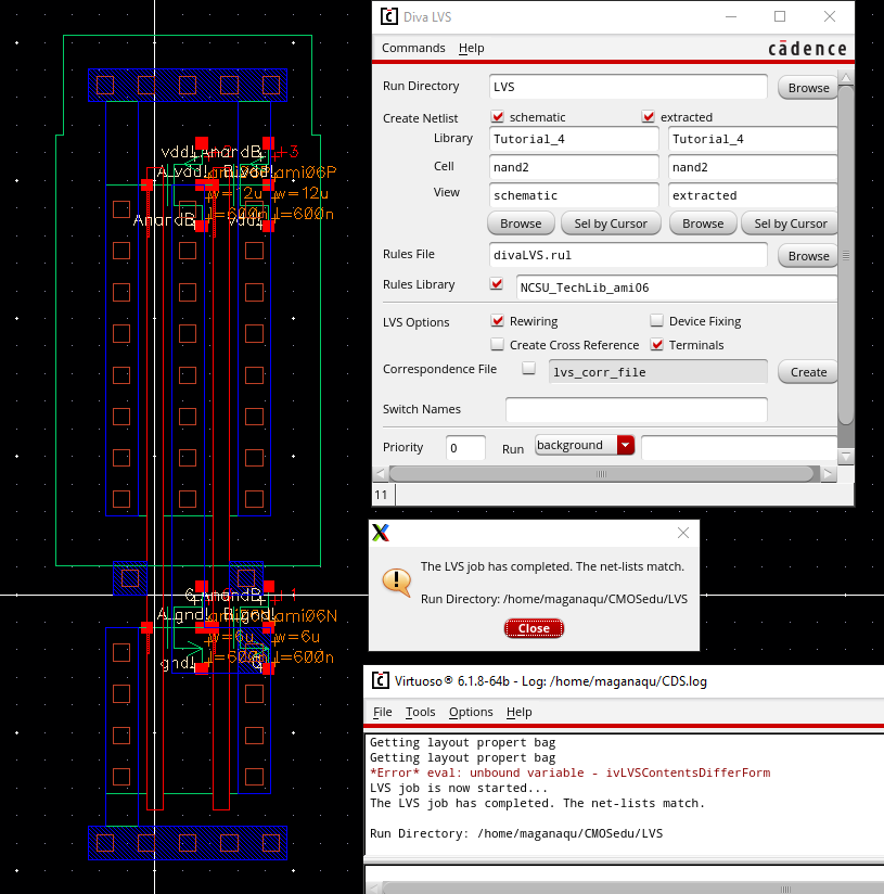
To finish this prelab, we have in the next picture with the extracted file with LVS verification
Lab Work
For the lab report, we are supposed to design, layout, simulate different components such as NAND, XOR and FULLADDER gates.
In the next picture you will notice the NAND gate looks very similar to the one from prelab, there is a small difference
we have the schematic of the NAND gate
Symbol of the NAND gate, but this one has my signature :D
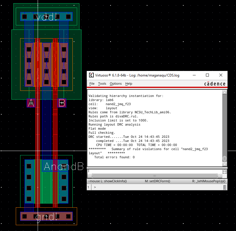
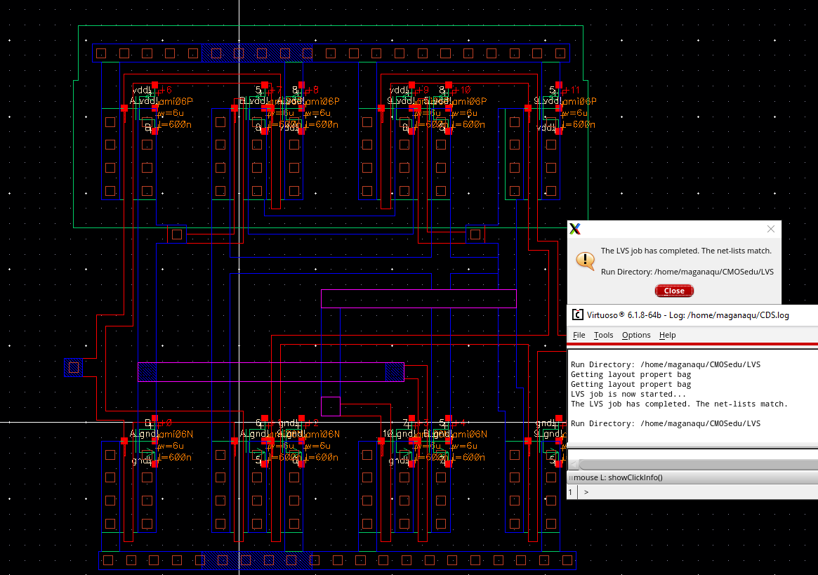
Now the layout with DRC, here is where the difference of the prelab comes
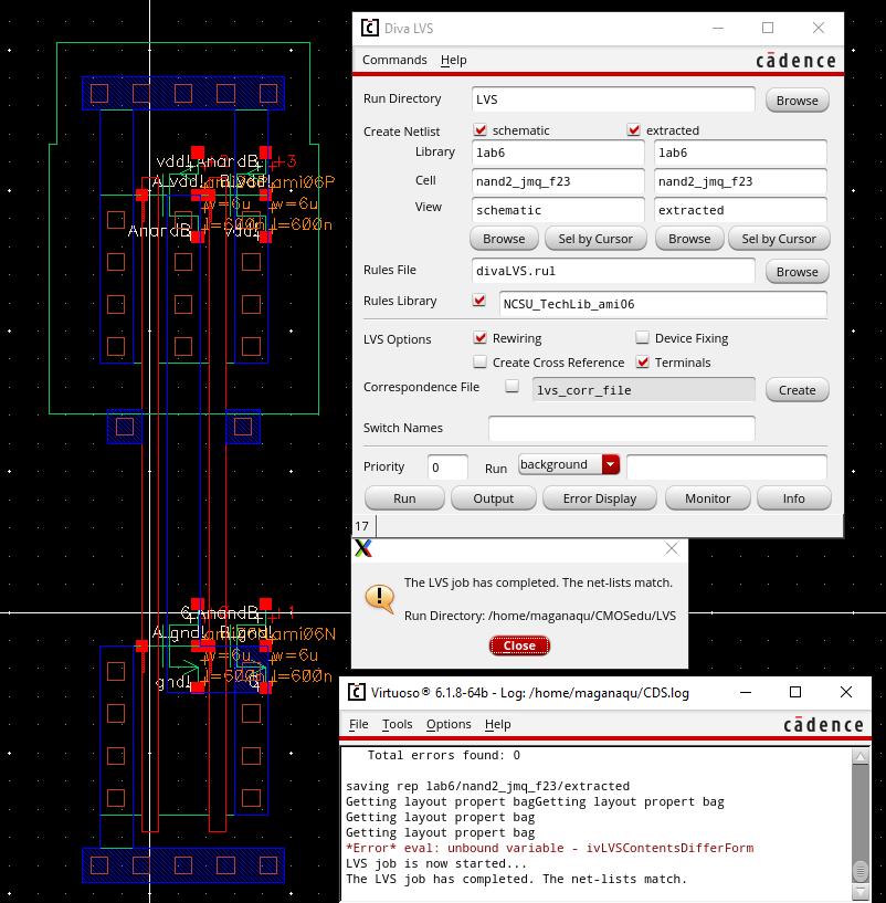
and extracted with LVS
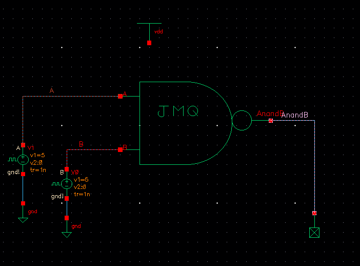
now, let's see how the simulation works. To test this NAND gate symbol. we'll use 2 inputs
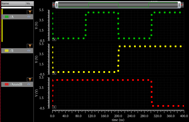
and the result... basically when A and B are 1, the output will be 0,
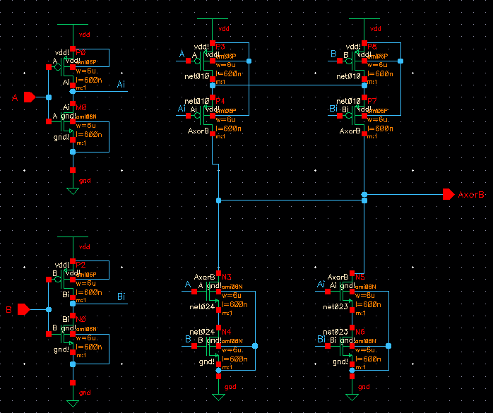
Now its turn for the XOR gate. Let's see our schematic first
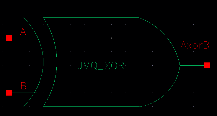
and symbol of the XOR gate with the respective signature
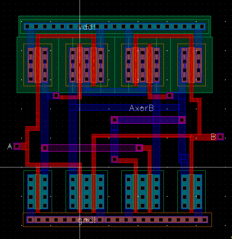
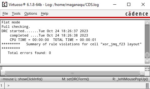
Now the layout with DRC
Next, our extracted with LVS
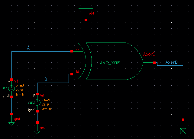
Finally, lets test our symbol with 2 inputs
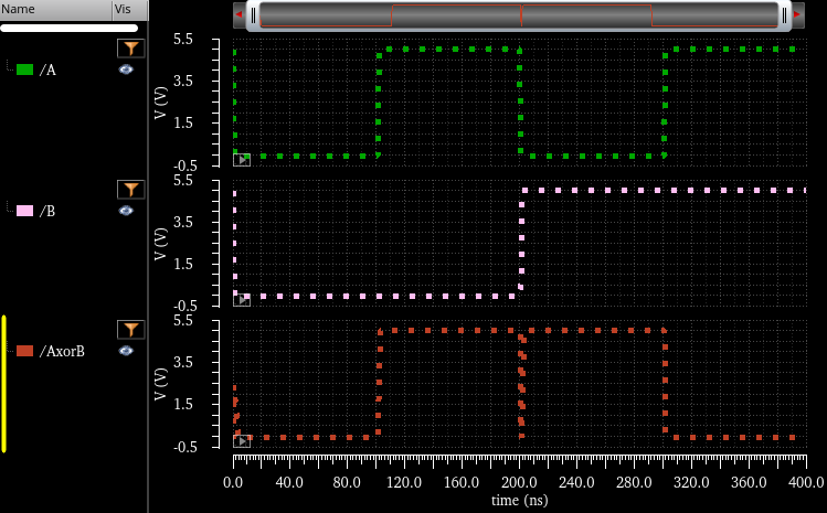
and we got the result that matches the normal behavior of the XOR gate
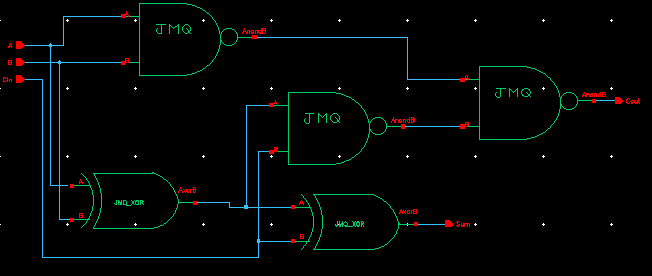
To finish this lab, lets show the last gate. First of all, we will take NAND and XOR gate that we created before on this
schematic
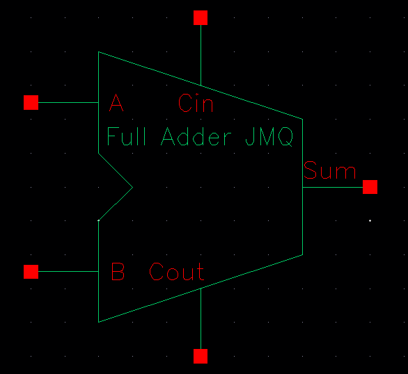
With that, now we are ready to make the symbol for the FULL ADDER gate as can see below
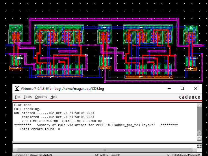
After that, in the next picture we can see the layout of the FULL ADDER, as well as DRC
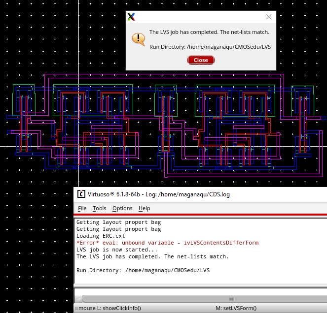
LVS is also important, so lets have the extracted one.
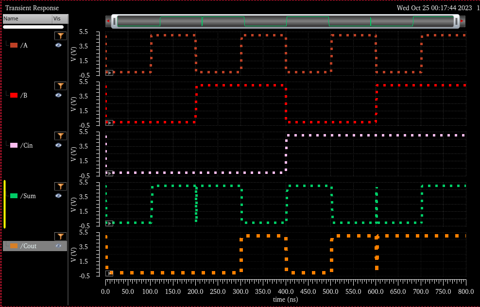
Now, we are ready to make the circuit for testing our FULL ADDER
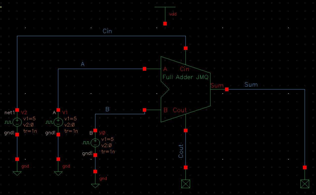
and this is what we got when we simulated. this match the normal behavior of the full adder
| A | B | Cin | SUM | Cout |
| 0 | 0 | 0 | 0 | 0 |
| 0 | 0 | 1 | 1 | 0 |
| 0 | 1 | 0 | 1 | 0 |
| 0 | 1 | 1 | 0 | 1 |
| 1 | 0 | 0 | 1 | 0 |
| 1 | 0 | 1 | 0 | 1 |
| 1 | 1 | 0 | 0 | 1 |
| 1 | 1 | 1 | 1 | 1 |
Back up
Return to EE 421L Labs