Lab 4 - ECE 421L
Authored by Josue Magana Quezada
Email: maganaqu@unlv.nevada.edu
09/27/2023

Prelab
For this prelab we will follow the same process of backing up our previous lab work as well as following Tutorial 2 that
is basically focused on NMOS and PMOS. We will use LVS to double check if they match.
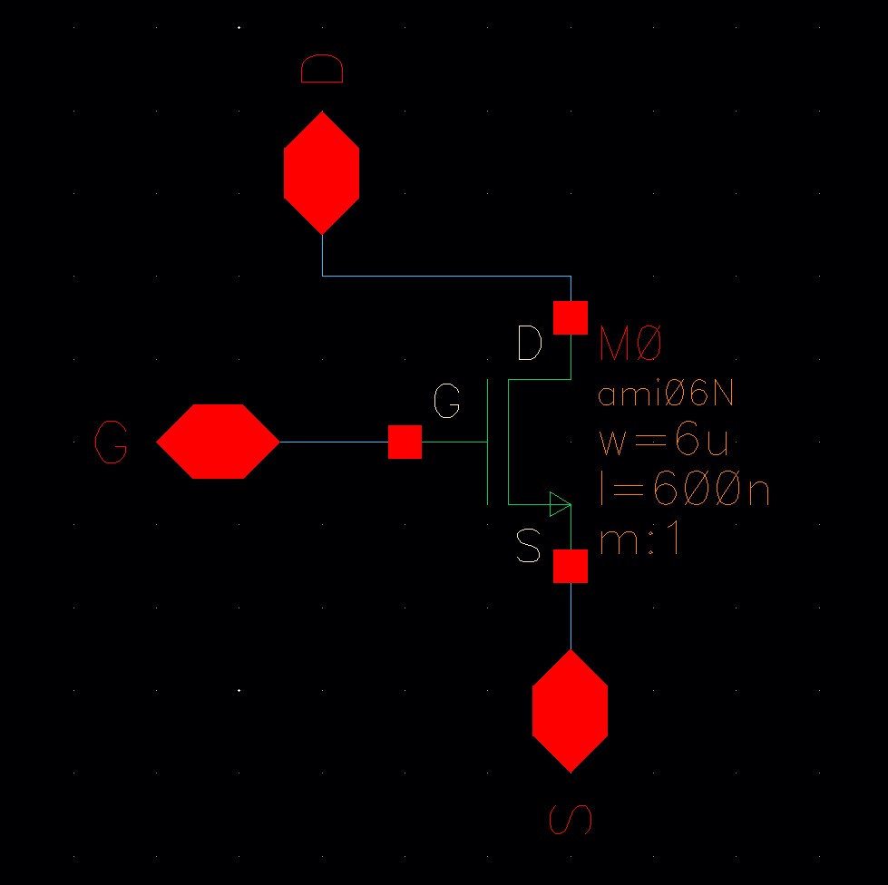
For Tutorial 2 we create a shematic and symbol for our NMOS as seen below
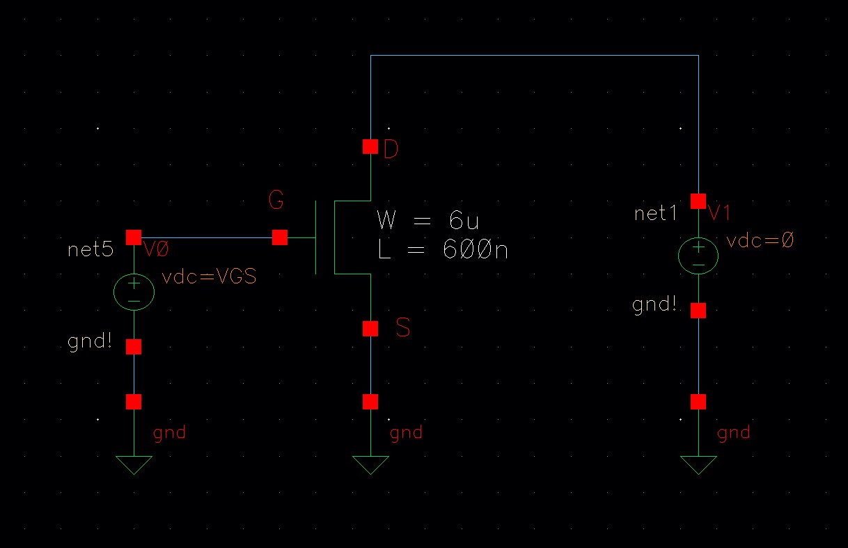
A circuit with our symbol
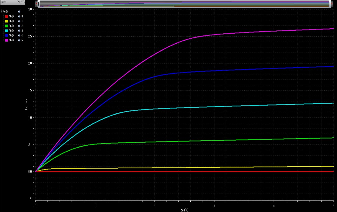
There's a section to see how to run Parametric Analysis on Tutorial 2, we are supposed to get something like this
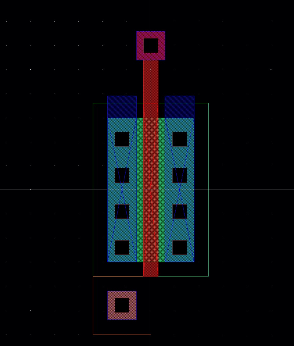
This is the layout of my NMOS
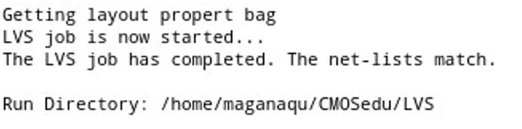
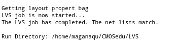
and then we run our LVS to check if our net-lists match
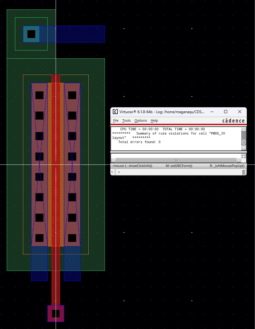
Once NMOS is done we can move forward to create our PMOS, here is the layout with the respective DRC verification
Lab Work
The
initial task we need to undertake involves the generation of four
distinct simulations. These simulations are divided equally between
two
types
of devices: NMOS and PMOS. On the other hand, for the PMOS device, we
will be operating under the assumption of a 12u/600n ratio.
PMOS, or P-type Metal-Oxide-Semiconductor, is another type of MOSFET, but it operates using positive carriers (holes)
For
the NMOS device, we will be utilizing a ratio of 6u/600n. NMOS, or
N-type Metal-Oxide-Semiconductor, is a type of MOSFET (Metal Oxide
Semiconductor
Field Effect Transistor). The operation of NMOS is based on the use of
negative carriers (electrons) for conduction
These simulations are crucial for understanding the behavior and performance of these devices under different conditions.
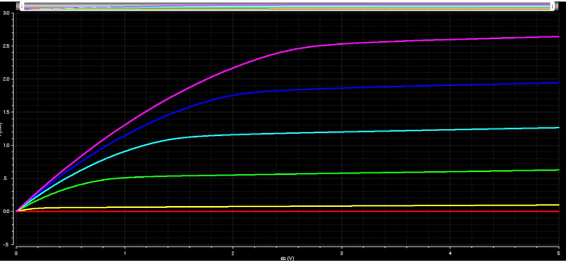
Here's our NMOS frm 0 to 5V in 1V step
Parametric analysis...
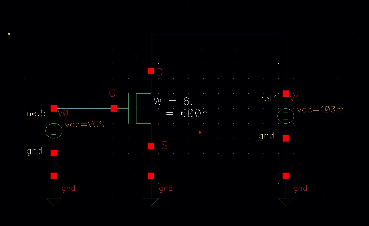
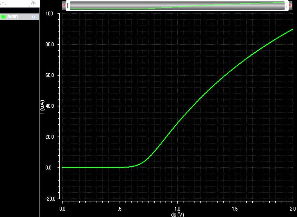
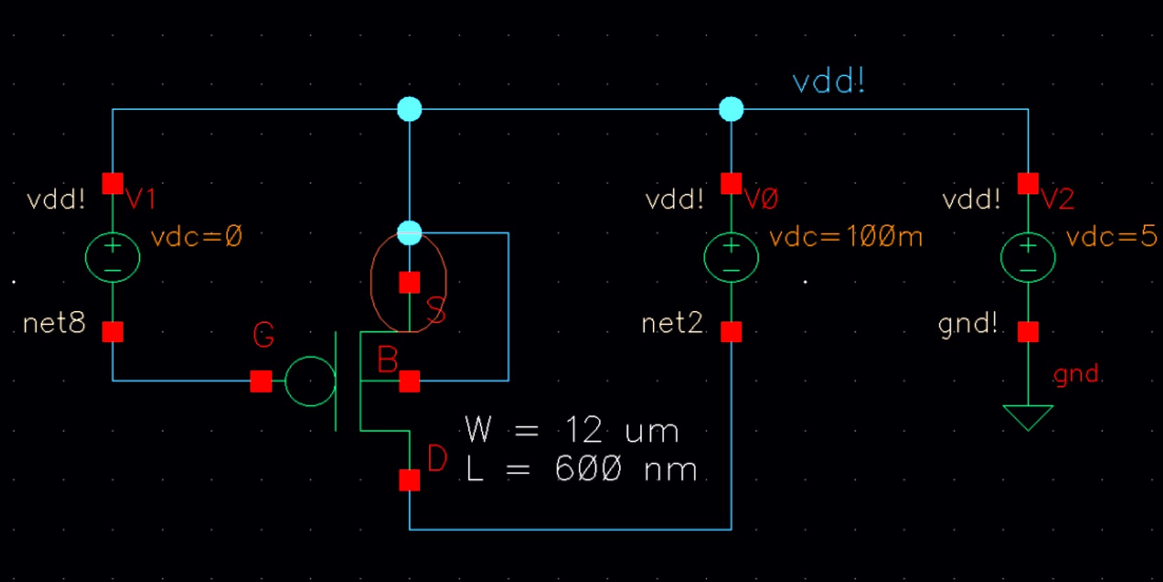
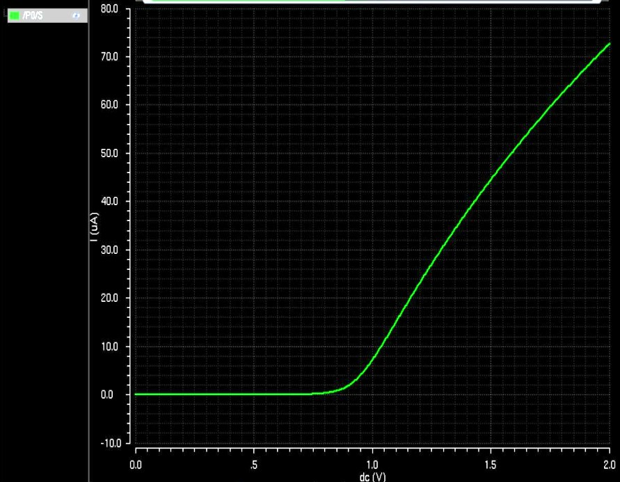
Now VDS instead of 0, it will be 100mV for this step also this one will from 0 to 2V of VGS
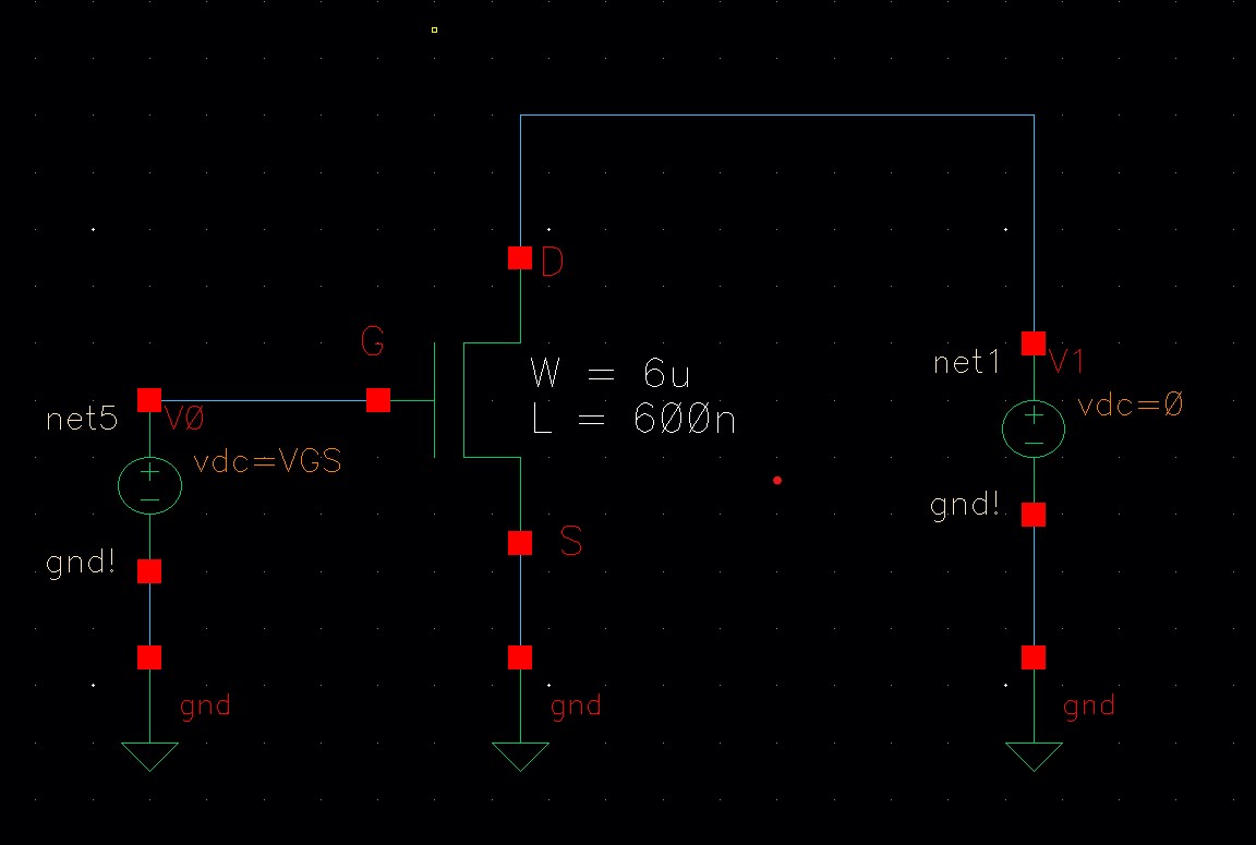
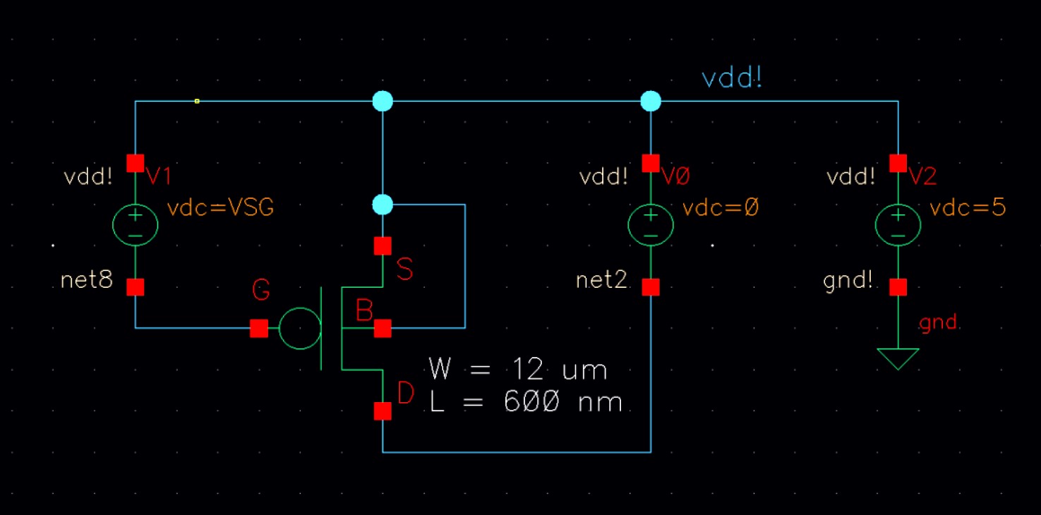
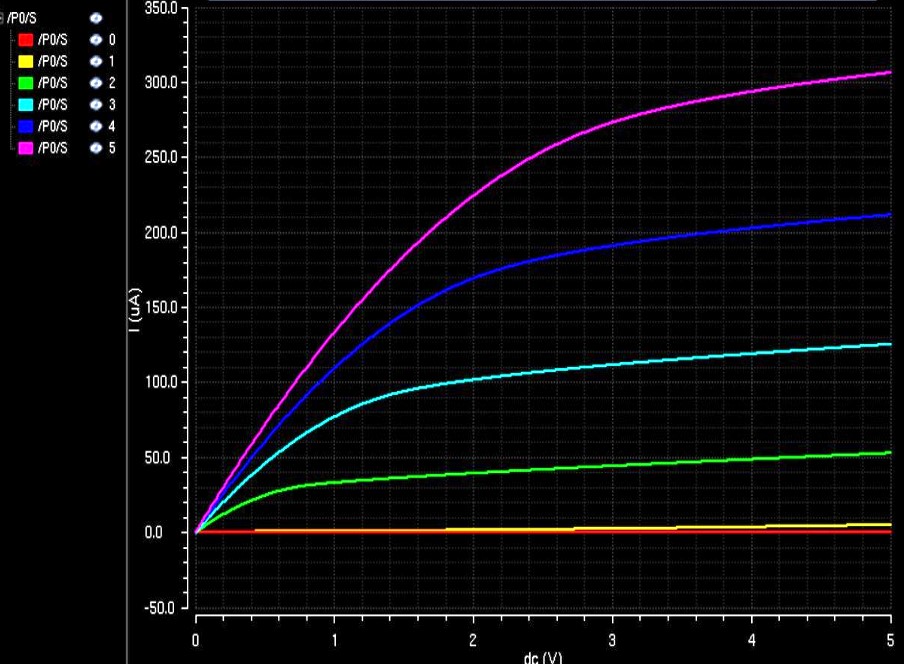
Next, i changed the schematic of PMOS device for VSG from 0 to 5 in 1V step. here i use 12u/600nm width to length ratio
Now VSD= 100mV. VGS from 0 to 2V in 1mV steps
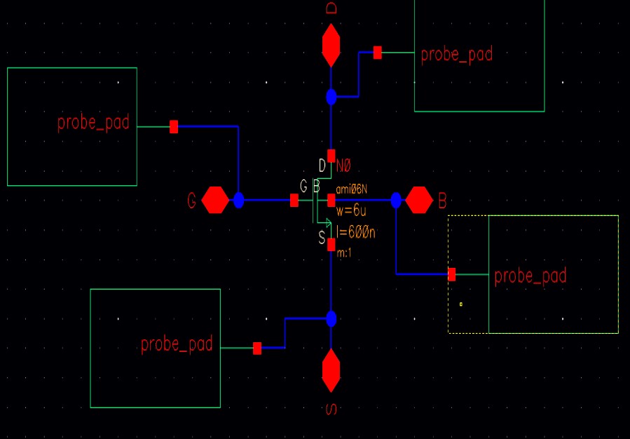
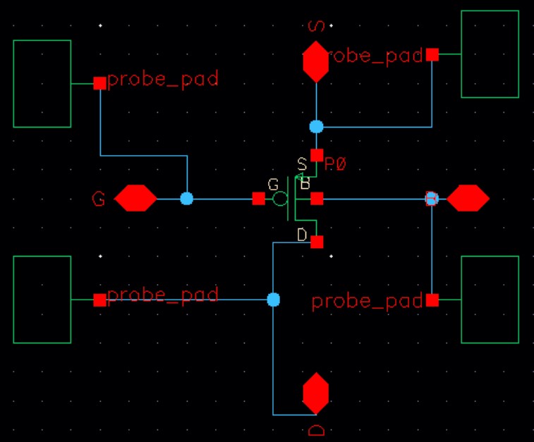
After allt his, we will create our layout for probe pad, with those we can create our circuit for NMOS as seen below
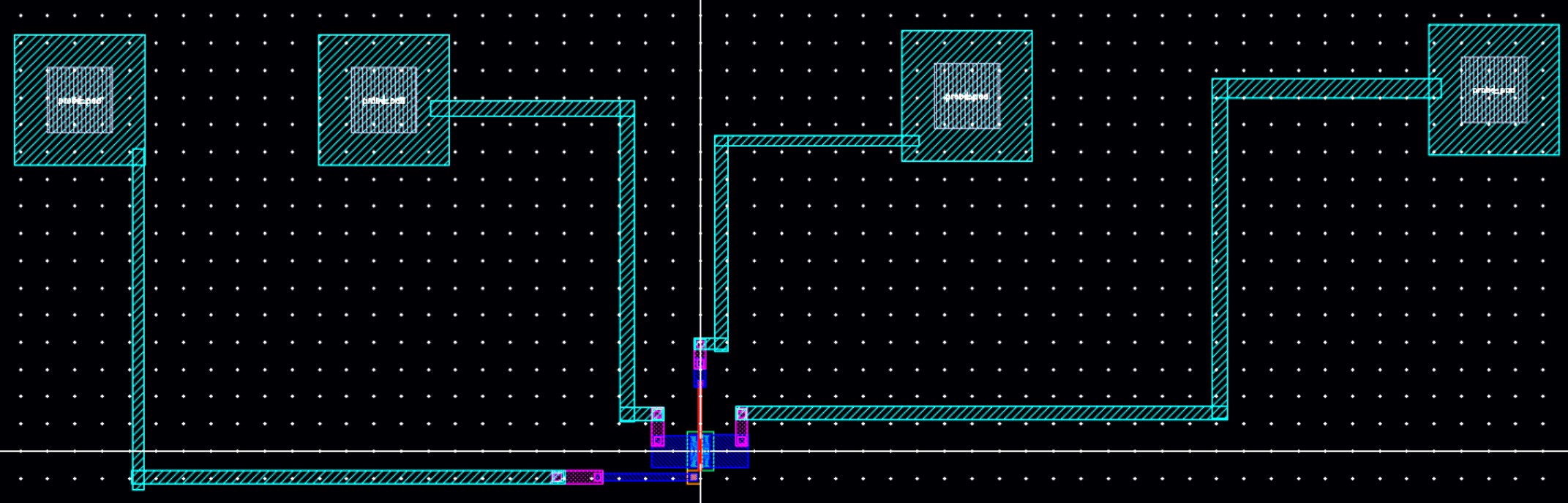
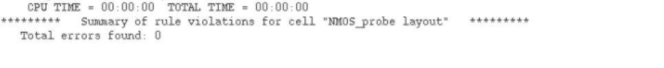
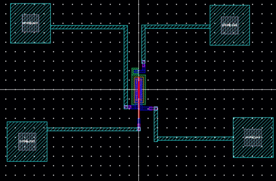
Now we are able to create the layout of the NMOS, as well as having our DRC verification
We will follow the same process but now for our PMOS
Layout of that schematic
For this one, we are able to LVS our schematic and extracted view.
Back up
Return to EE 421L Labs