Lab 3 - ECE 421L
Authored by Josue Magana Quezada
Email: maganaqu@unlv.nevada.edu
09/20/2023
Lab
description
We are going to Layout DAC from lab2 on this practice
ZIP FILE
Lab3

Prelab
First
of all, we will back up all our previous lab practices, this might help
for different things such as reference for future lab reports.
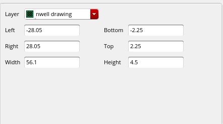
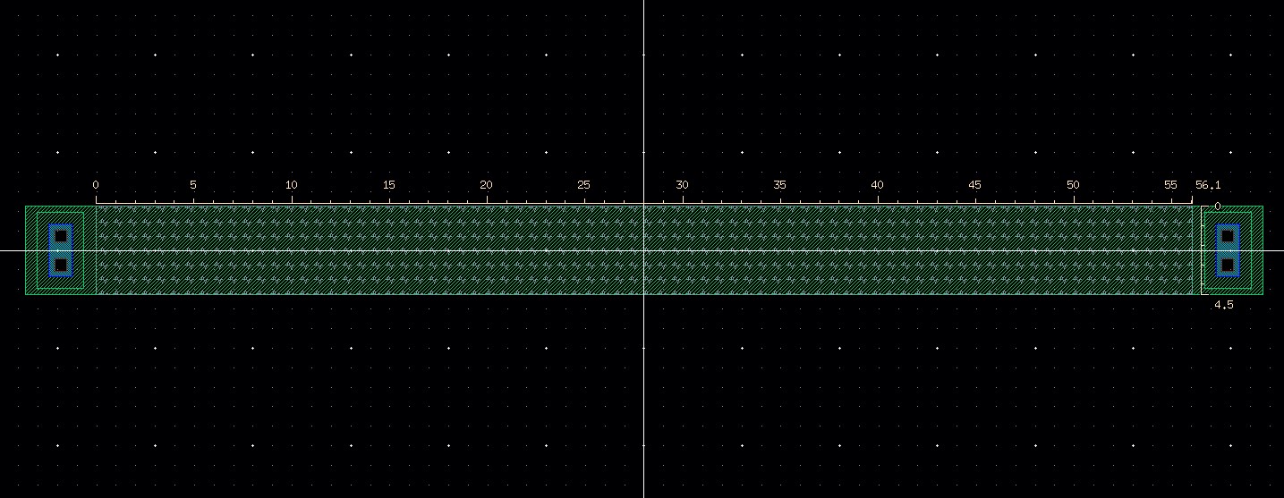
I made a layout of the 10-bit DAC. I was supposed to create a 10k resistor.
To obtain the dimmensions, i used this formula and the next steps
R = Rd * (L/W)
R = 10k ohms
Rd = 802
W = 4.5 microns
10k = 802 * (L/4.5 microns)
=> L = 56.1 microns
Below is a picture of the resistor properties in Cadence.
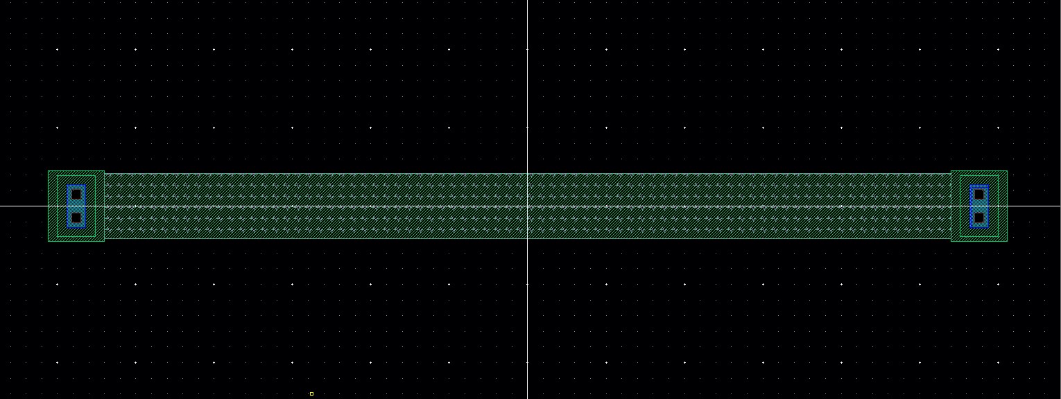
my resistor
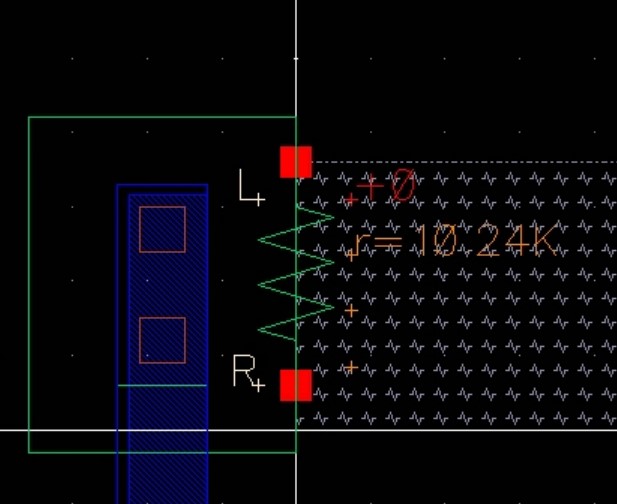
extracted resistor, reflecting our 10k
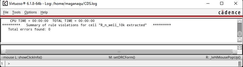
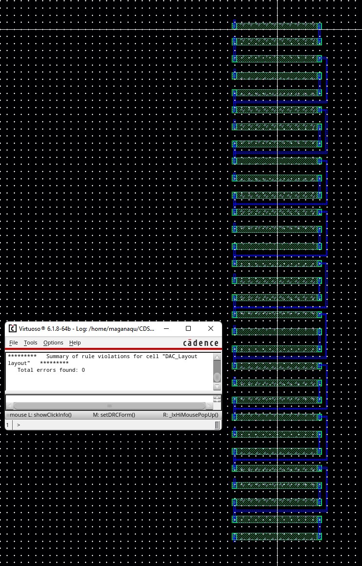
Also our DRC to verify everything is correct
Lab Work
We will use a ruler to measure our resistor manually
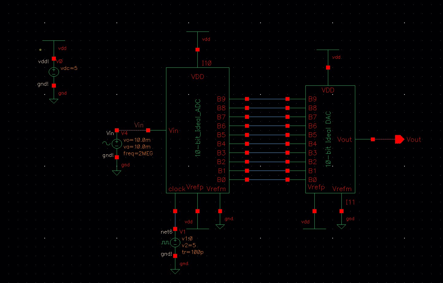
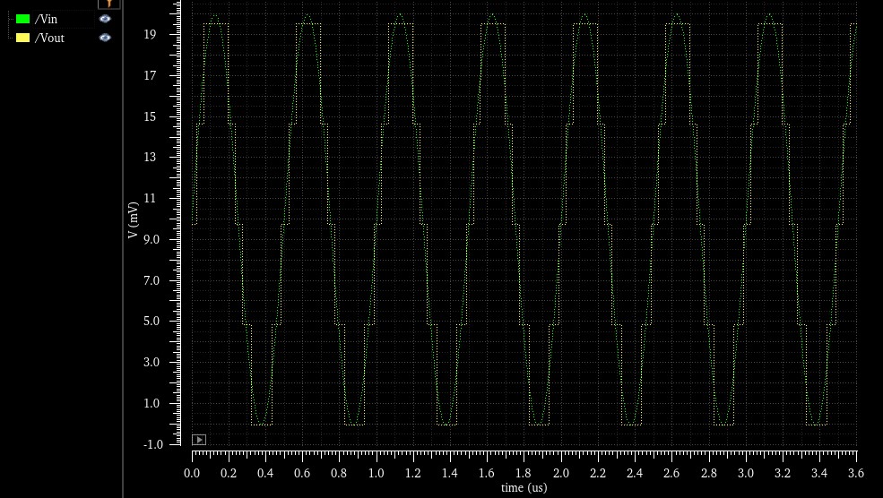
The
next pictures were from Lab 2, and they show the schematic and
simulation of the DAC under no load conditions. It shows to work
correctly
Now we are going to Layout our DAC with N-wells, it will be making 31 N_well resistors . The minimum separation is 5.4um.
Once we set it up, we will verify with DRC. it is expected to obtain 0 errors.
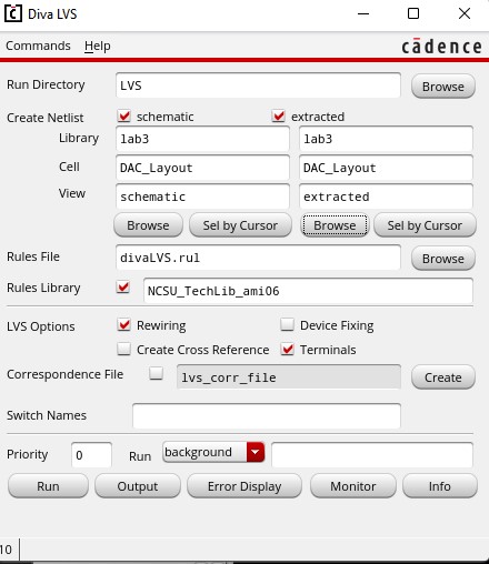
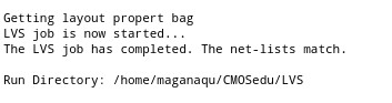
The
last step we will go to our extracted DAC -> Verify -> LVS, we
are going to compare it with our schematic and it is supposed to match
all the net-lists
Back up
Return to EE 421L Labs