Lab 2 - ECE 421L
Authored by Josue Magana Quezada
Email: maganaqu@unlv.nevada.edu
09/13/2023
Lab
description
For
this lab, we will design a schematic view of a cell

Prelab
Get lab2.zip on your desktop.
Inside, there's a simulation with a perfect 10-bit Analog-to-Digital Converter (ADC) and Digital-to-Analog Converter (DAC).
Put this zip on the server you use with Cadence, like Tutorial_1 or CMOSedu.
Make sure you have the NCSU Cadence Design Kits.
Unzip it and add this line to the cds.lib file in the design folder (if it's CMOSedu): DEFINE lab2 $HOME/CMOSedu/lab2

Start Cadence from the design folder.
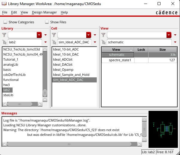
Use the Library Manager, go to the lab2 Library.
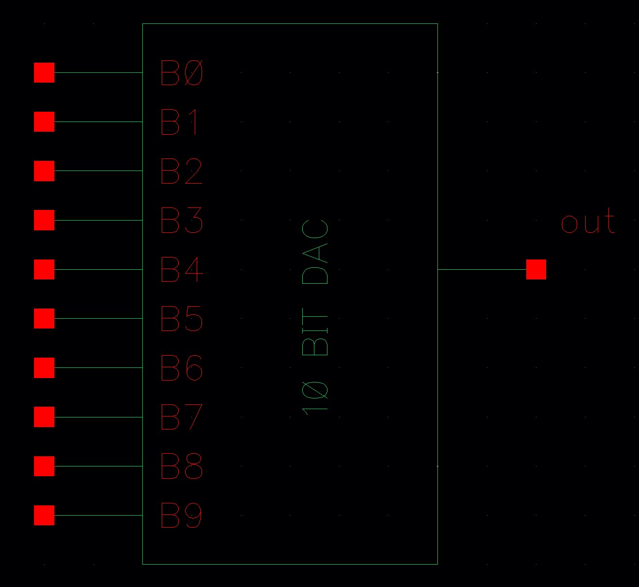
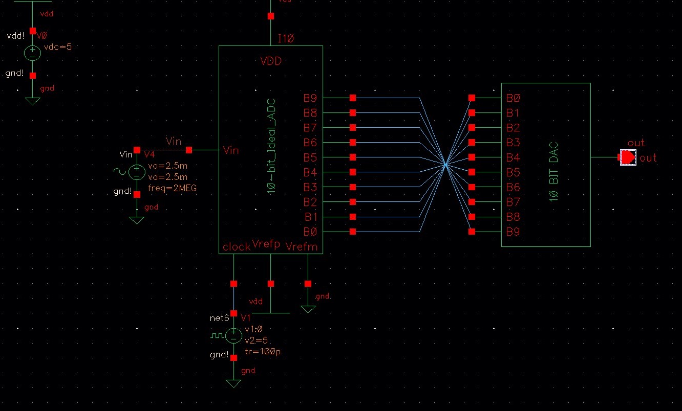
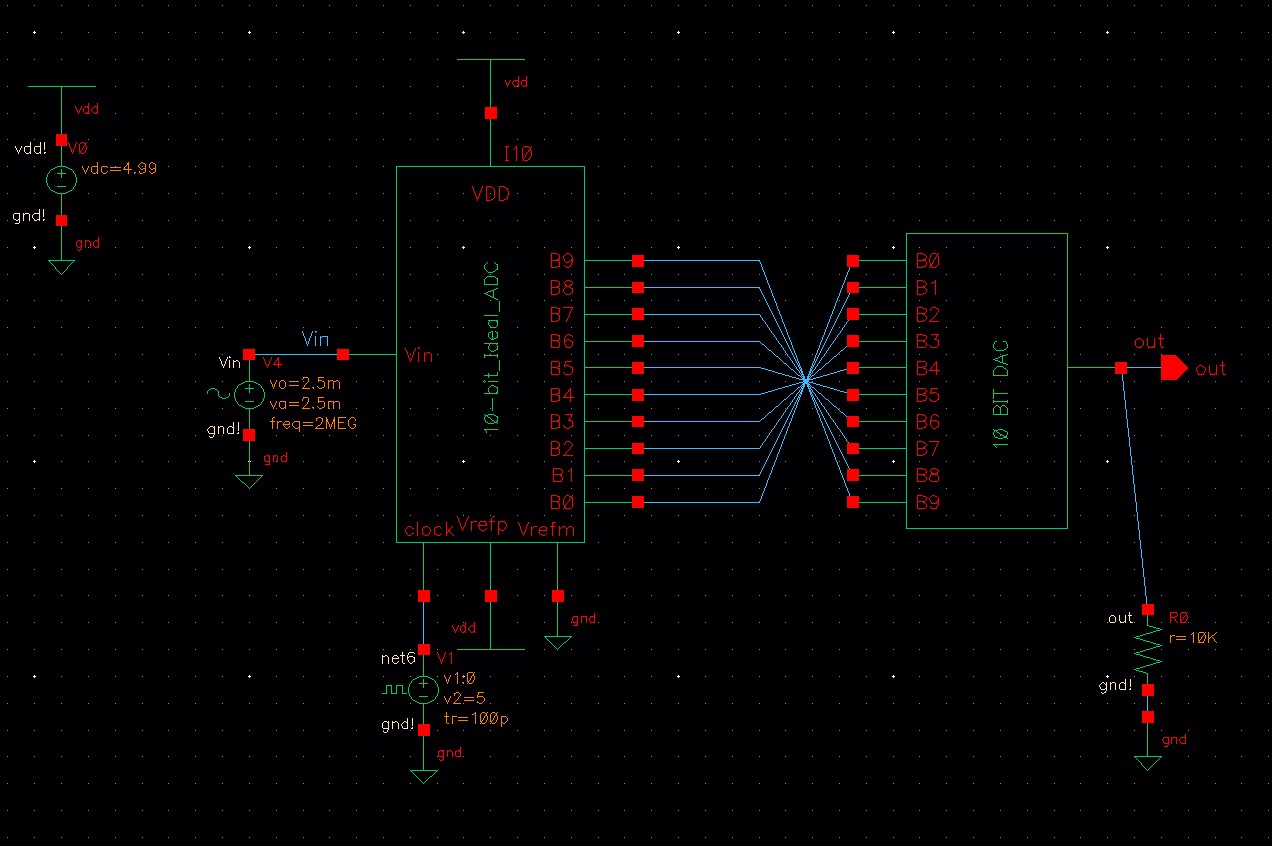
Open the schematic of sim_Ideal_ADC_DAC.
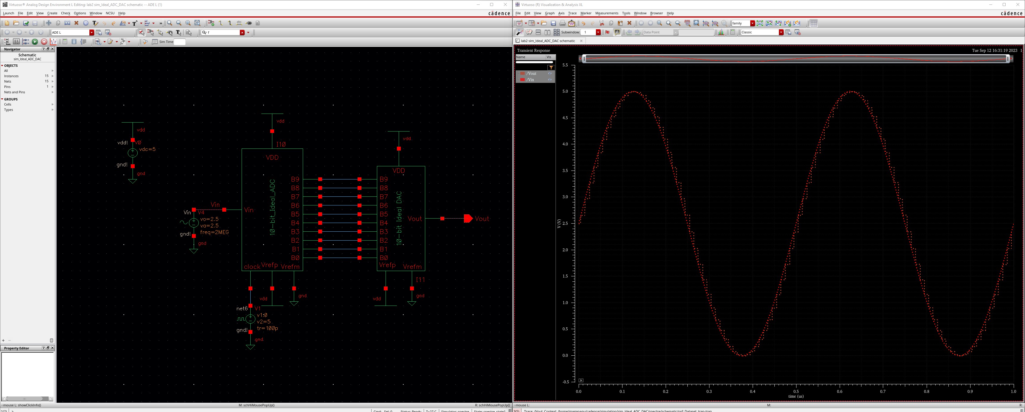
This cell has the ideal 10-bit ADC and DAC
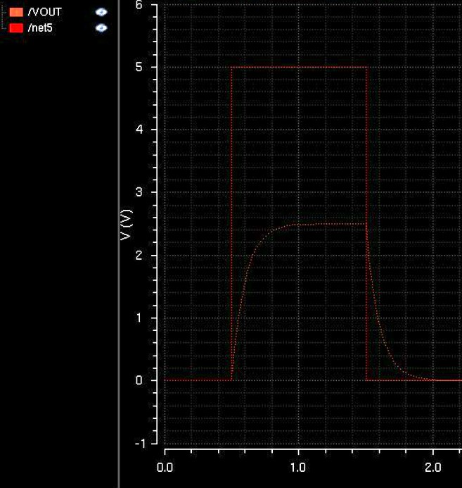
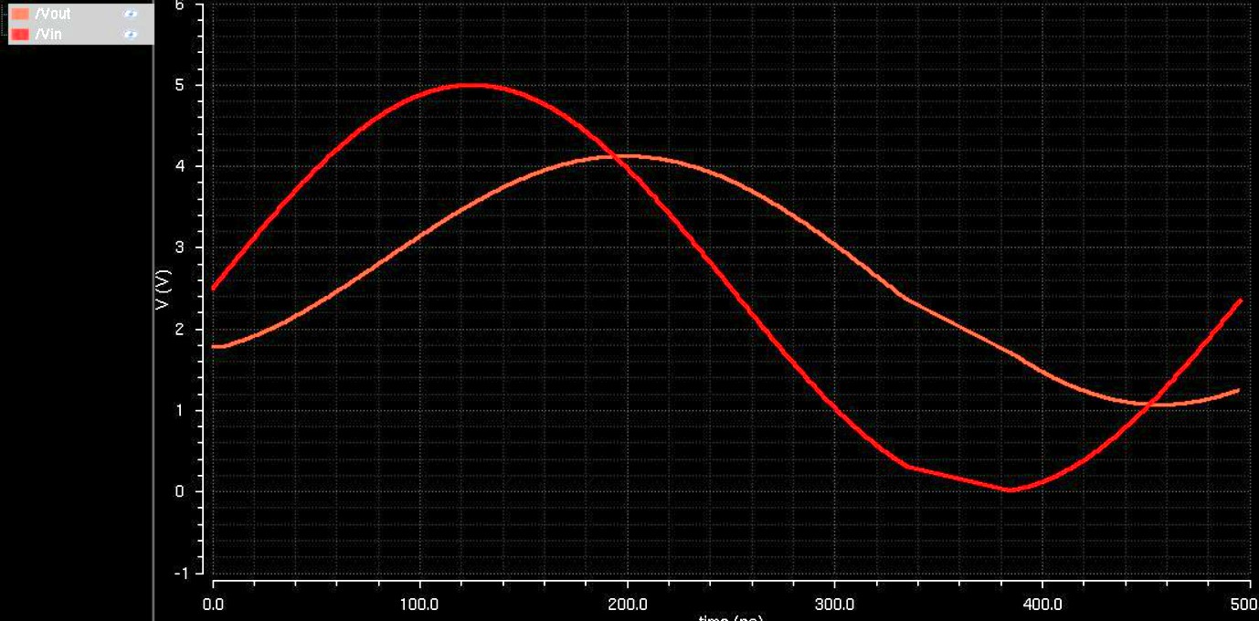
I opened the schematic shown on the left and on the right you can see the result of the loaded state
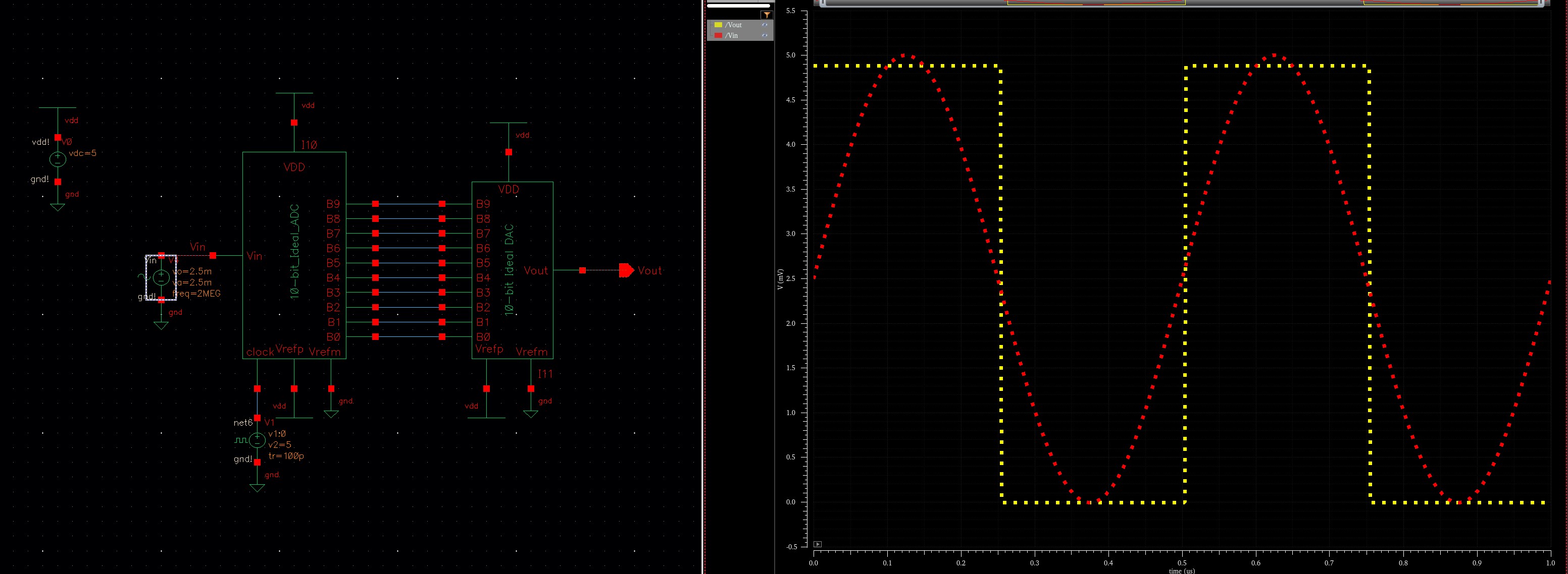
I modified the waveform, this was made by changing the value of the input Voltage for 5mV
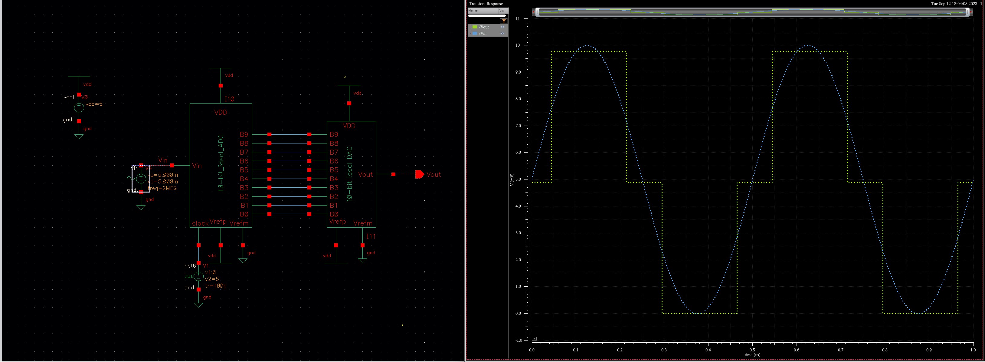
When
calculating LSB = VDD/2^N ==> 5V/2^10 ==> 8.88mV. this is our
Least Significant Bit. Now will be able to see our minimum voltage for
B[9:0]
Lab Work
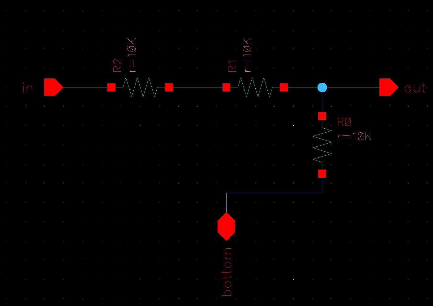
To begin with, we will start designing a DAC 10K N-well. This will be simple...
First we create the schematic with 3 resistors of 10k as shown in the next picture
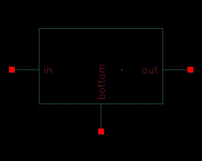
Next we'll create the symbol based on that schematic. As a reminder: go to Create / Cellview / From Cellview
you will notice another screen will show up with your symbol :D
Once
we have our symbol, we can use this one for the next schematic. This
will be a cascading 10 of the 1-bit DAC. dont forget to create your pins
such as I, OUT aand BOTTOM
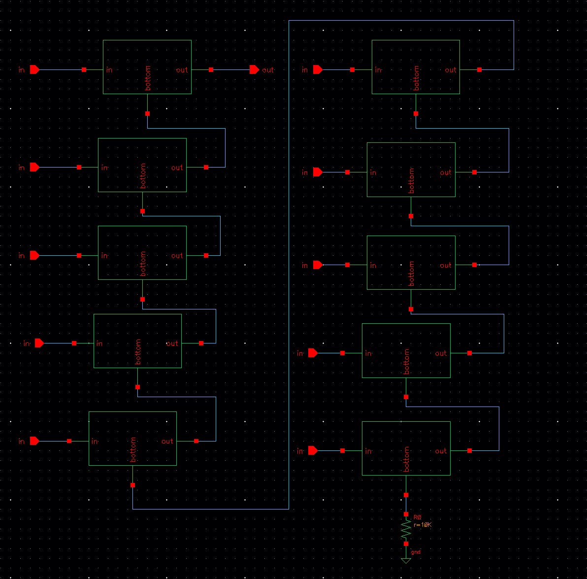
Same story to create the symbol from this schematic (Create / Cellview / From Cellview) and you will have the coming design in your screen
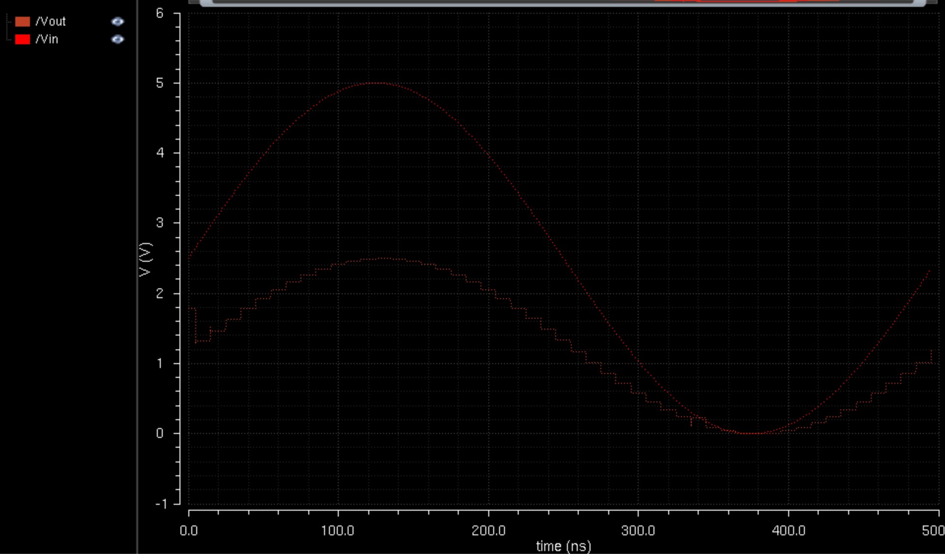
Now
we will create a Delay. adding a capacitor on Vout of 10p and From B8
to B0 connected to the ground. As well as adding a pulse voltage from 0
to 5. 0.7 RC we'll get a
waveform as the shown in the next picture
Now,
we are going to have copy of the ideal ADC TO DAC. From that schematic
we will remove the 10butDAC so we can add the one we made previously.
Once it is ready
the next step is simulating the waveforms
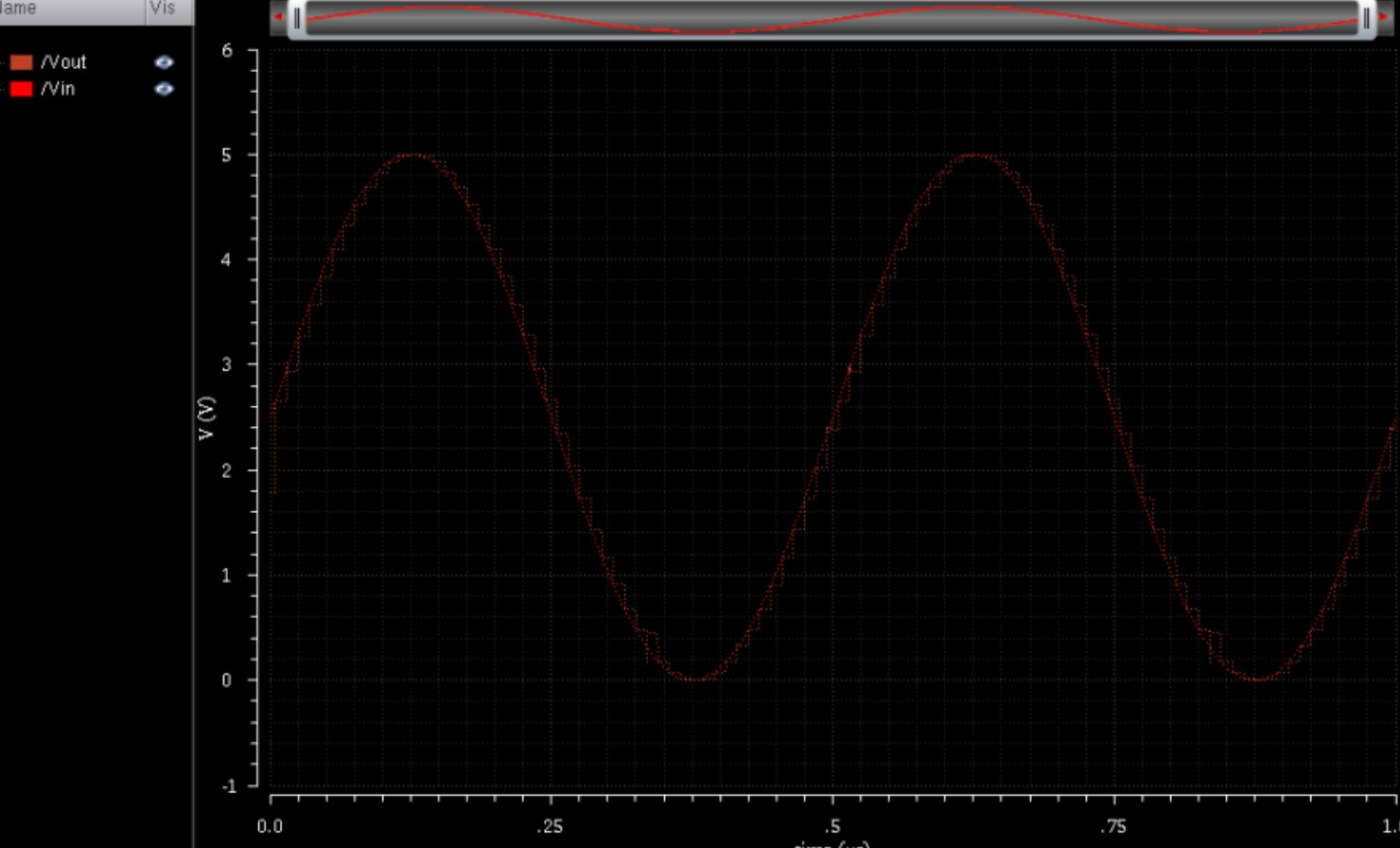
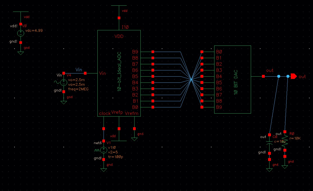
Same thing but now with a 10pf Capacitor near of Vout
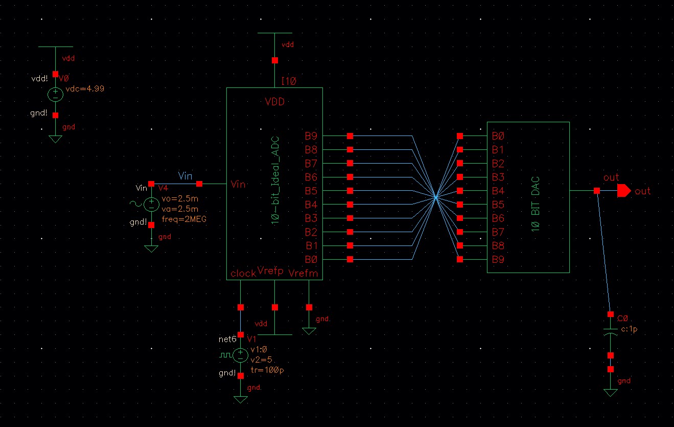
Adding a 10k resistor
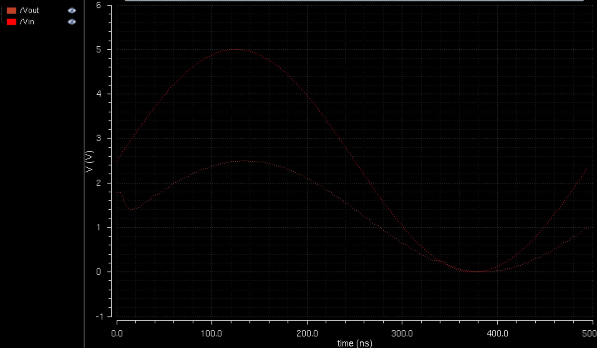
And finally a parallel RC. We will notice there is a dlay in the output, also the amplitude gets certain changes
To
finish this, i backup my files every 20min as a safe method of loosing
progress. it is basically sending the files to my school email.
Conclusion
When
we add resistance, Vout becomes smaller but stays in sync with Vin.
Adding a capacitor delays Vout, making it lag behind. Using both
reduces Vout and adds a time delay.
Return to EE 421L Labs