Project
Authored by Josue Magana Quezada
Email: maganaqu@unlv.nevada.edu
11/22/2023

- Project (NOT a group effort) – design a non-inverting buffer circuit that presents less than 100 fF input capacitance to
- on-chip logic and that can drive up to a 1 pF load with output voltages greater than 7V (an output logic 0 is near ground
- and an output logic 1 is greater than 7V). Assume VDD is between 4.5V and 5.5V, a valid input logic 0 is 1V or less, a valid
- input logic 1 is 3V or more. Show that your design works with varying load capacitance from 0 to 1 pF. Assume the slowest
- transition time allowed is 4 ns.
FIRST HALF
To begin
with this project, there are multiple steps to complete in order to get
the expected results from the Project description.
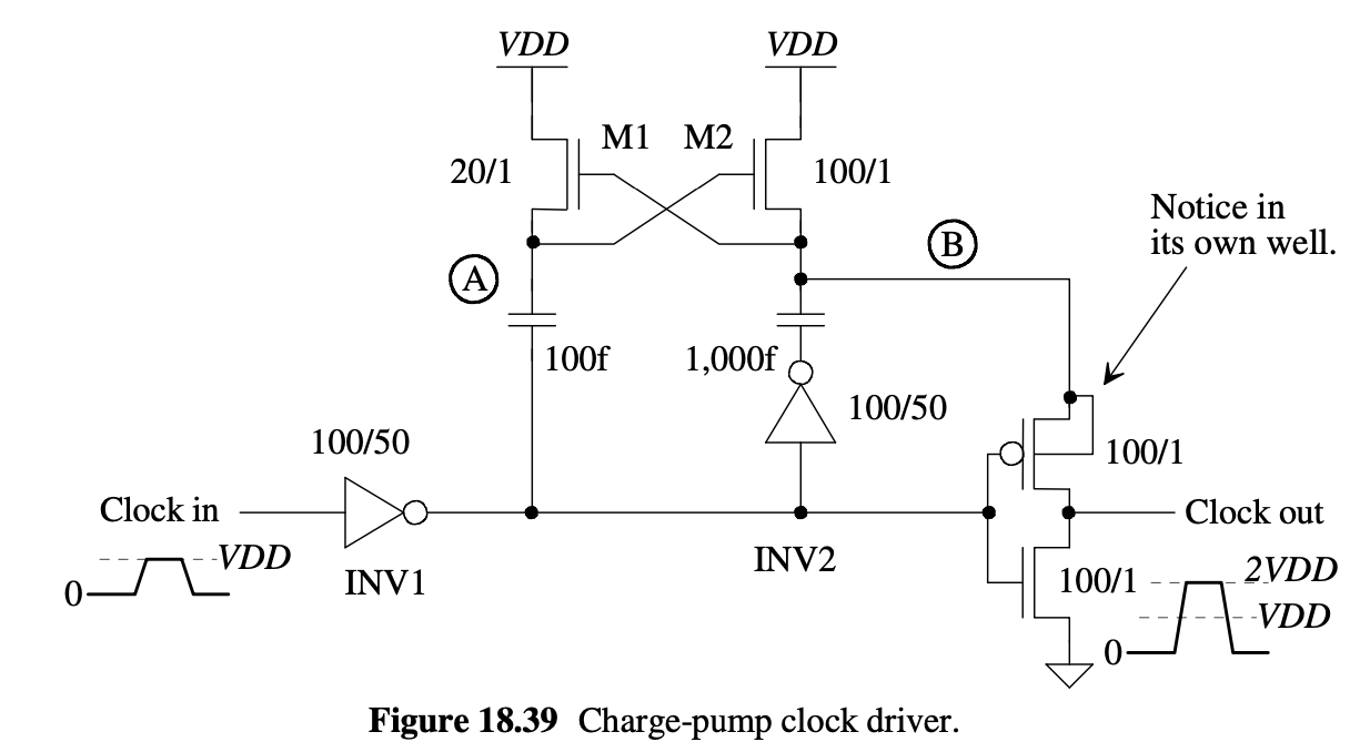
A good
reference is following circuit on Figure 18.39 from 4th Edition CMOS
book. Just remember that for this project we are supposed to use C5
process.
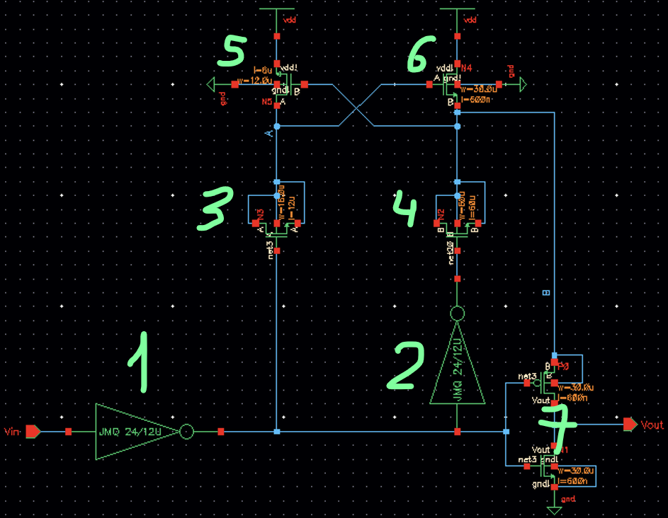
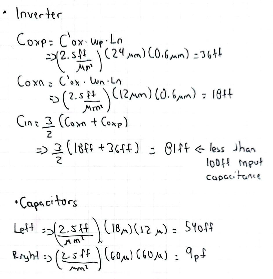
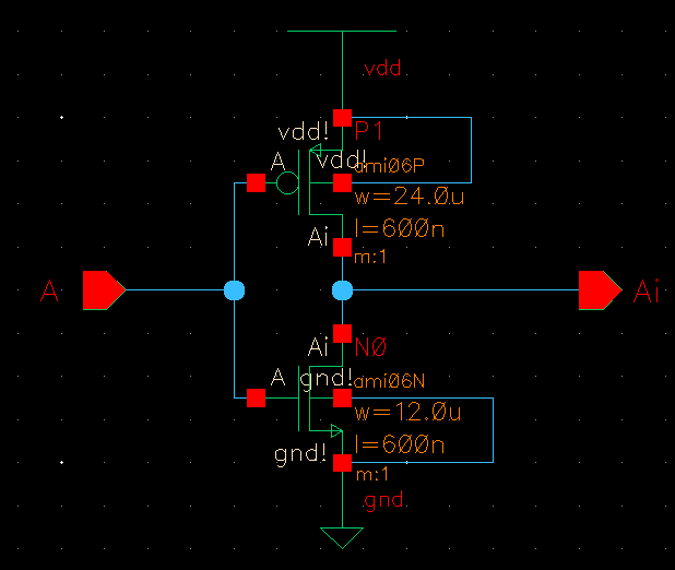
The 1st part of handcalculations for the size of our inverters, and i ended up choosing 36ff for PMOS and 18ff NMOS
This will result in 81ff input capacitance, which means is less than the condition of this project (100ff)
For
the 2nd part, we're using MOSFETs as special capacitors in our circuit.
These MOSFETs can act like capacitors because of Strong Inversion.
To
make these MOSFETs act as capacitors, we connect a few parts together
in a specific way in the circuit. We also calculated how big these
"capacitors"
need to be. We made one of these "capacitors" on
the left side have a size of 540fF. This helps to push a point in the
circuit closer to 2 times the Vdd voltage at its
highest point.
This part of the circuit switches between two voltage levels: 2 times
Vdd and just Vdd, but they're like mirror images of each other.
This is the circuit with the updated properties
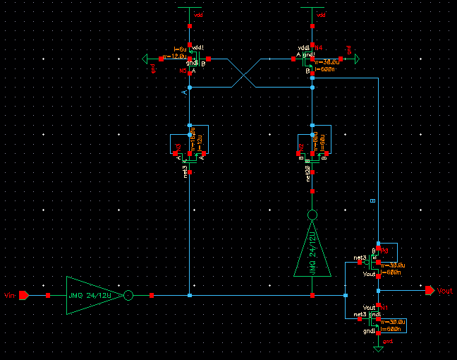
(closer look)
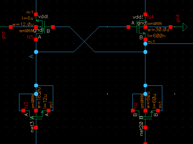
As you can see there is a symbol of the inverter in the schematic above, lets take a look of what is inside
Here we have the values previously calculated:
Now lets verify that our logic low will be less than 1V
In the next table, you will see how the lowest switching point is 2.173V and highest one 2.756V
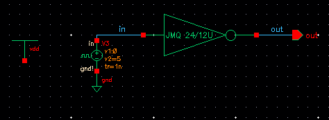
Setup for the inverter simulations | 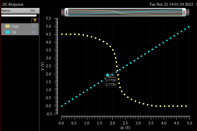
4.5V input. switch point 2.173V |
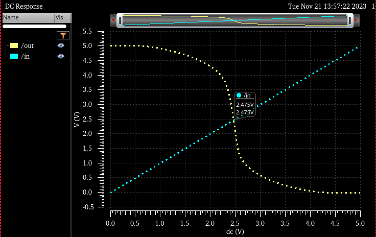
5V input. switch point 2.475V | 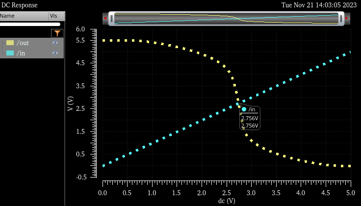
5.5V input. switch point 2.756V |
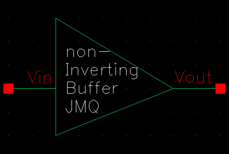
The next symbol represents our Non_inverting_buffer
Now lets compare the results of different VDD when our Non_inverting_buffer has no load
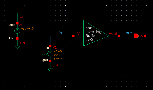
VDD: 4.5V
out: 8.8V | 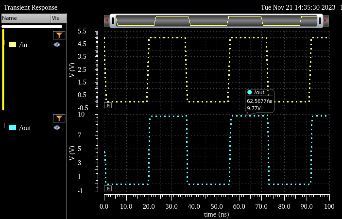
VDD: 5V
out: 9.77V |
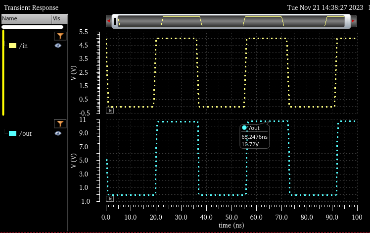
VDD: 5.5V
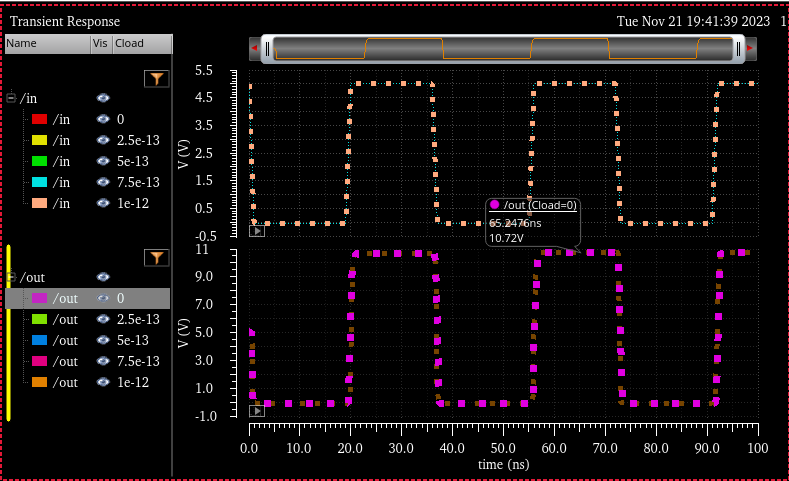
out: 10.72V | 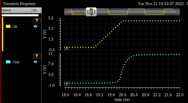
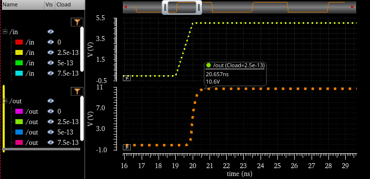
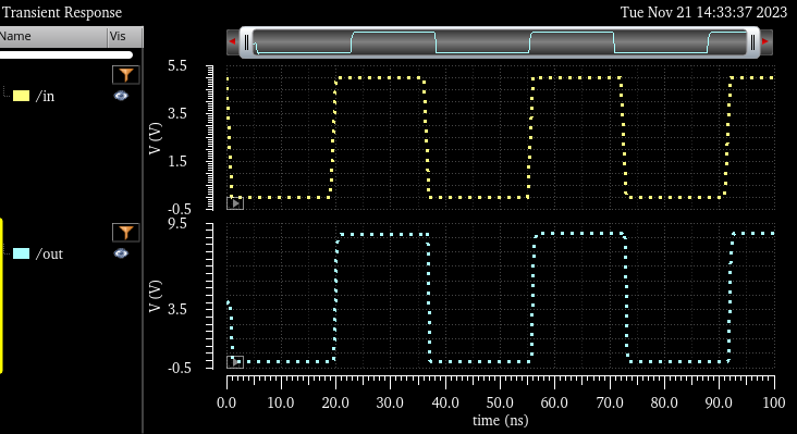
Here we can see the difference of delay time is less than 4ns |
now lets add some load by following the next schematic
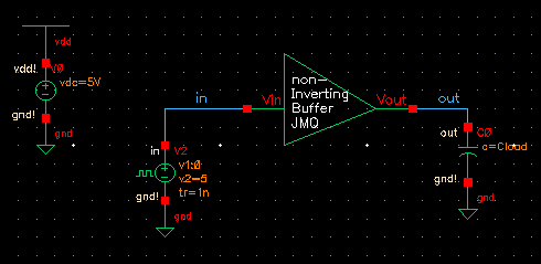
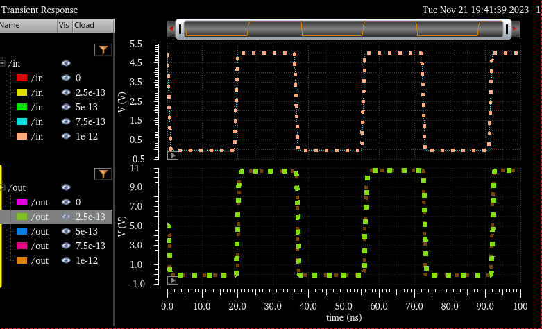
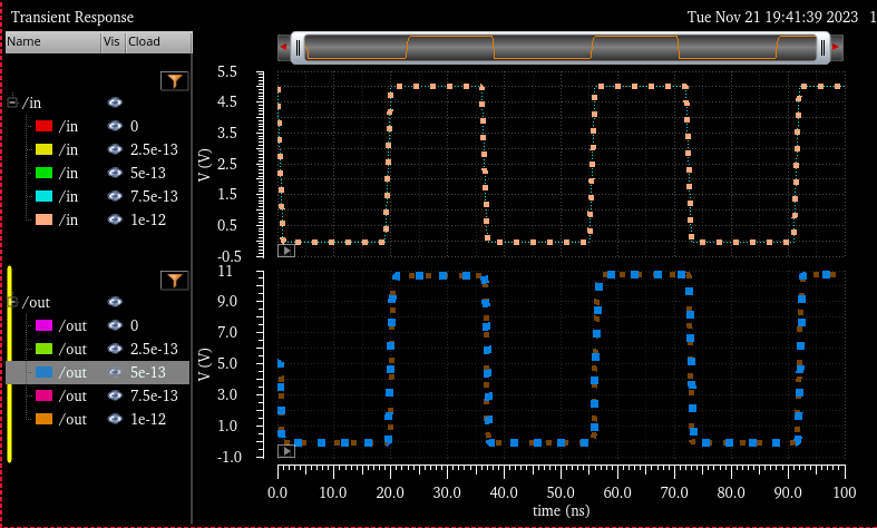
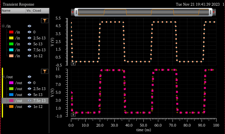
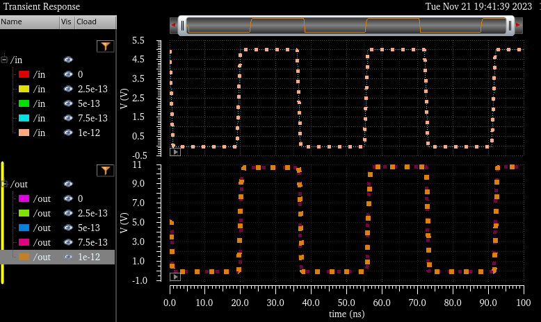
When using Cload, we can setup different cap values instead of having it one by one
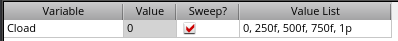
In
the next table we are able to see the results. All different loads did
NOT change at all, same V out (10.72V) as well as same delay time
(~2ns)
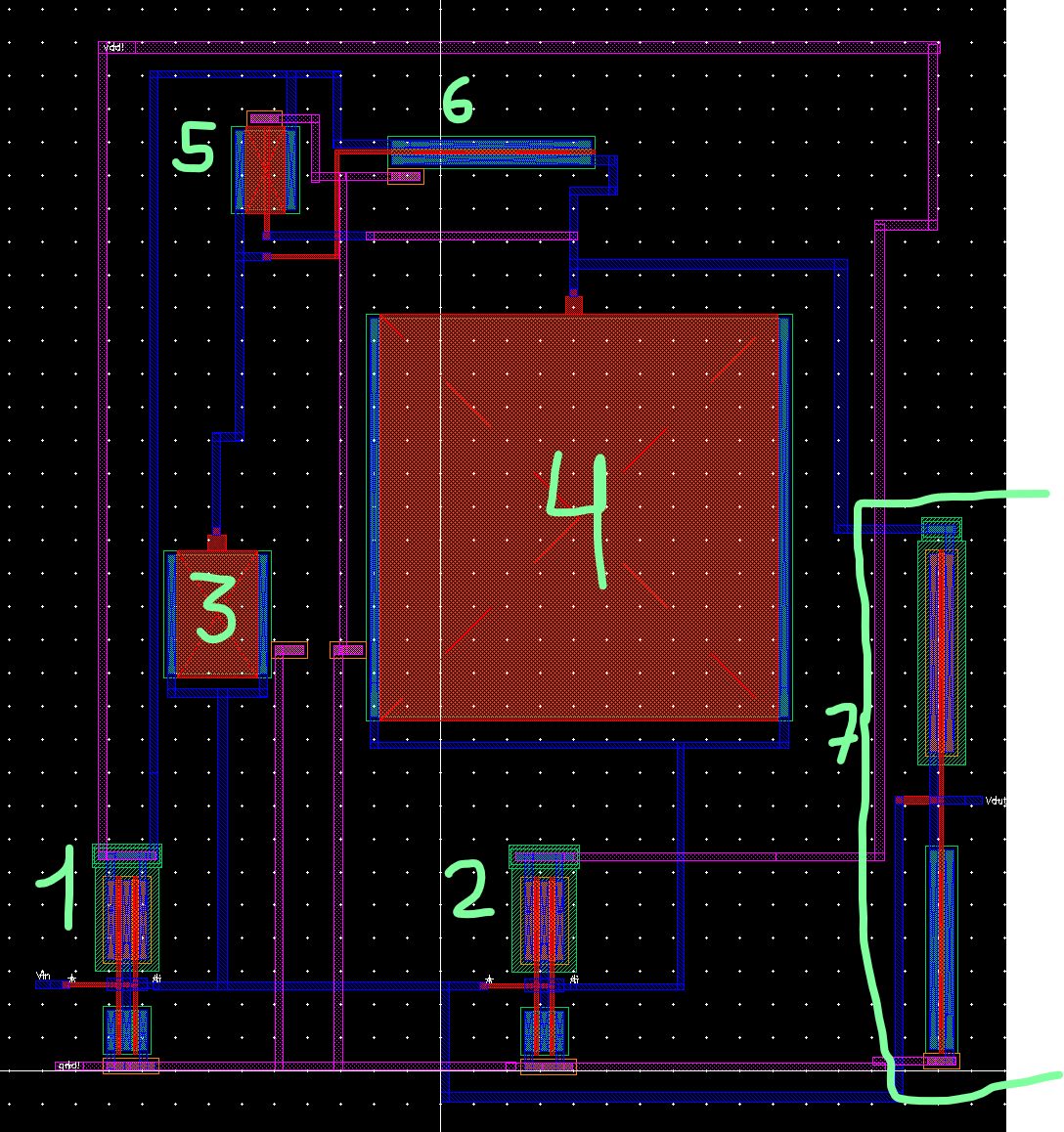
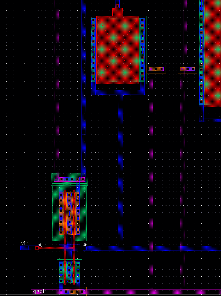
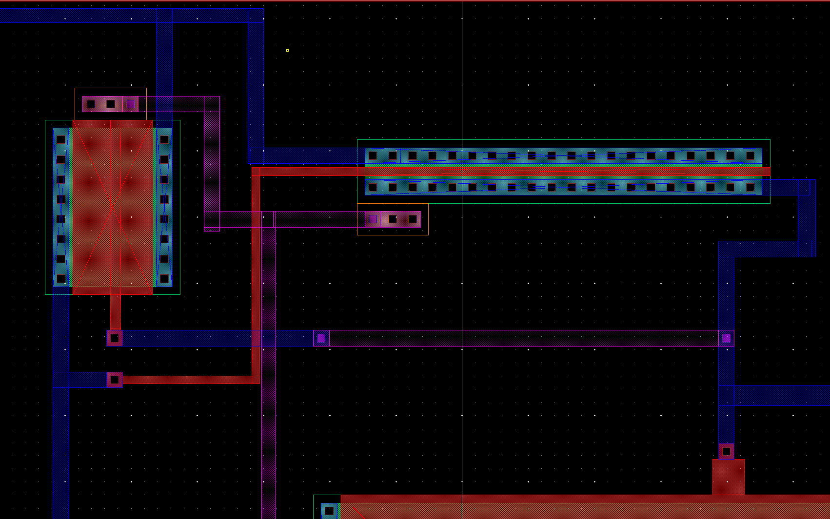
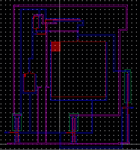
2ND PART LAYOUT
On the left wie have the schematic labeled and right the final layout
Some closer pictures
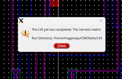
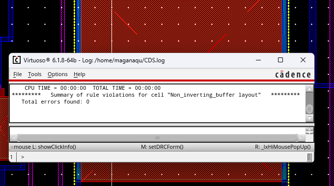
DRC verified
Extracted file
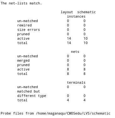
And finally LVS matched
ZIP FILE HERE!
Return to EE 421L Labs