Final Project - ECE 421L
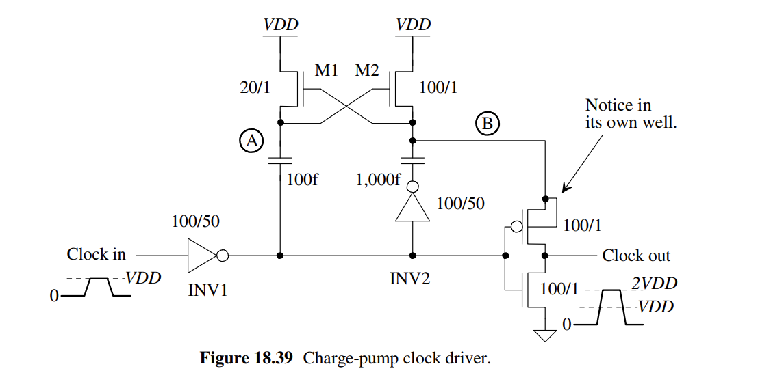
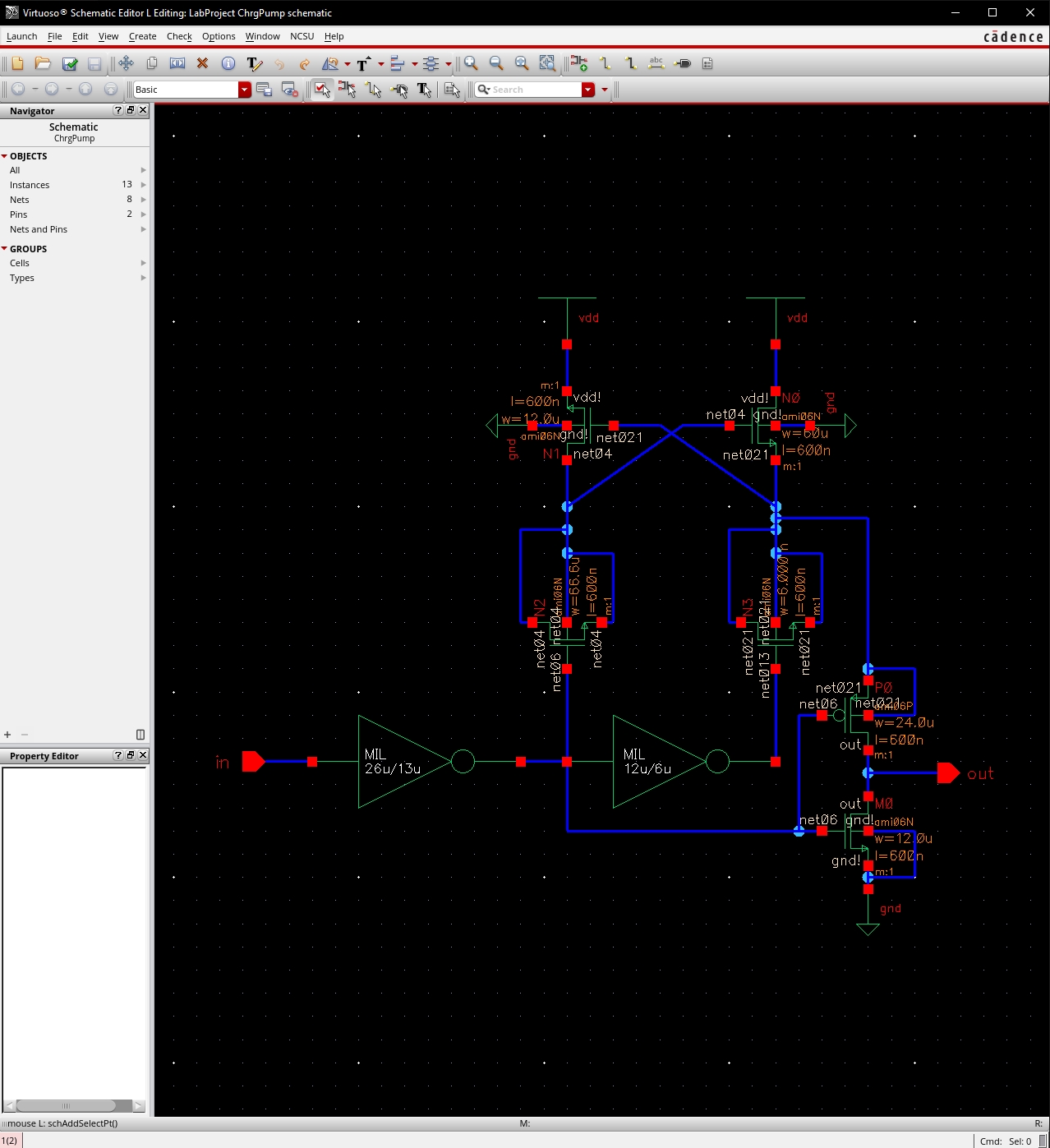
Input and Clock Signal: In this circuit, our clock signal oscillates between 0 and 1. Early in the circuit, there are two inverters that produce complementary clock signals, which are out of phase with each other. This means when the input VDD is high (4.5-5.5V), the first inverter (INV1) outputs a low signal, and when the input is low it outputs a high signal. When the input is 0, it's inverted to 1 (equivalent to VDD), which charges the smaller 100fF capacitor, well call it C0. This charged capacitor then activates a M2, which in turn charges the larger 1pF capacitor, called C1.
Charge Pump: C0 has a lower capacitance and as such holds less charge. Its primary function is to charge the M2 transistor switch, and prevent leakage currents that might unintentionally activate M2. It's essential that C0 has sufficient capacitance allowing enough time for C1 to fully charge up to VDD. If C0's capacitance is too low, it will limit the amount of charge held in C1, restricting the output voltage. On the other hand, C1, with its higher capacitance, is designed to accumulate more charge up to VDD, which is then used to boost the output voltage to 2VDD. When the input pulse switches to high, the bottom of the capacitor changes from 0V to VDD due to the inverter below it. Since capacitors release their charge gradually and not instantaneously, the voltage across C1 changes from VDD to 2VDD, effectively adding the stored charge of VDD in the capacitor to the VDD from the inverter, resulting in a total of 2VDD.
Output Stage: The final part of the circuit includes another inverter. When the input to this inverter is high, the gate of the PMOS transistor opens, allowing it to handle the larger current coming from the C1 capacitor. Conversely, when the input is low, the PMOS transistor is switched off, and the NMOS transistor instead pulls the output down to GND. This design ensures that the output alternates between 0 and 2VDD, matching the clock signal's oscillation.
Lab Report:
I used MOSFET's in strong inversion as the capacitors to reduce layout size and complexity. Strong inversion requires that VGS being greater than VTH, meaning electrons become attracted to the gate shorting the drain which will result in a plate forming for a capacitor. The capacitance per area is greater than a poly-poly capacitor, this is because MOSFETs Cox'(2.5/um^2) capacitance per area is much higher than the 900aF/um^2 of a poly-poly capacitor.
Calculations:
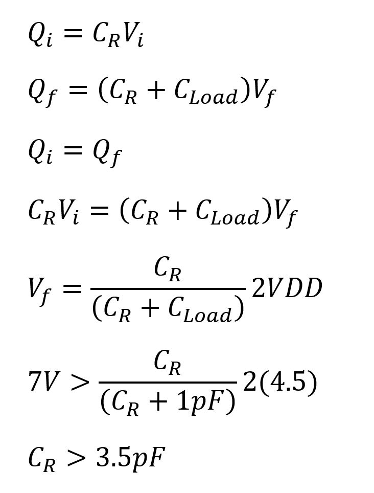
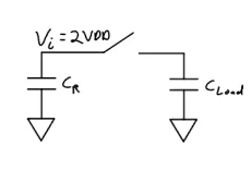
We need VDD to
work from 4.5-5.5V so in the formula we plugged in the worst-case scenario of
4.5V and the lowest acceptable Vf at 7V.
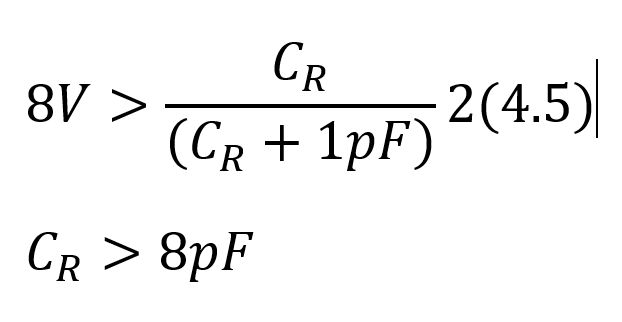
We could shoot for
a more reliable voltage of 8 to ensure that our logic 1 is not lost due to
manufacturing issues but that would also make our design significantly more
complex as to size the MOSFETs we end up with either a massive Wn of
6mm for 8pF or we would use a 60µm by 60µm.
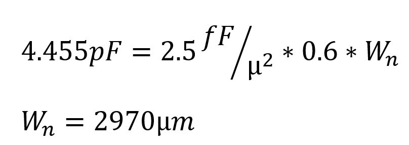
I decided to use an Wn 2970µm to not change the Ln of 0.6µm.
This allows me to ensure that I can layout a Wn 55µm with a
multiplier of 54 giving me 4.455pF which exceeds the minimum value of 3.5pF we
calculated to ensure proper operation at >7V.
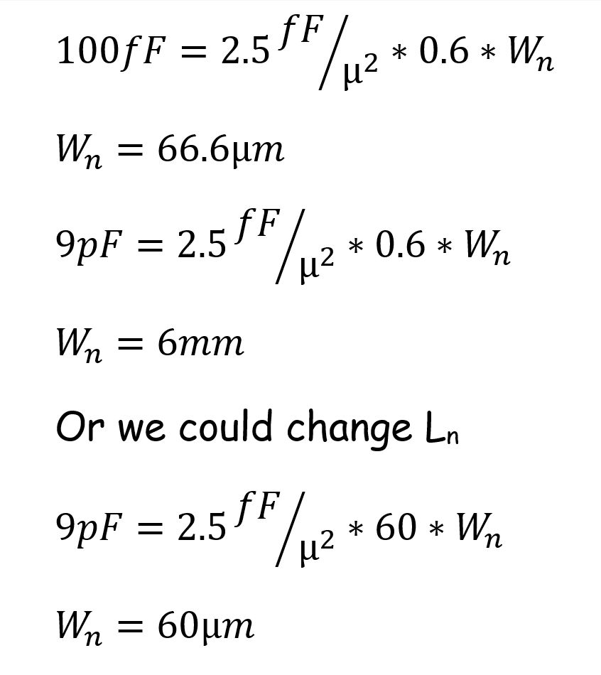
Or leaving Ln but choosing a value that allows us to use the multiplier and stay on grid.
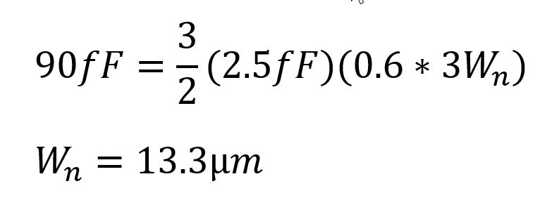
For choosing the size of our input inverter we need to ensure that Cin < 100fF using the formula below.
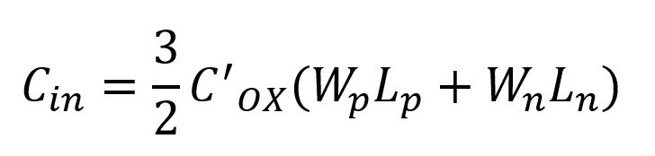
For setting our TPHL and TPLH the same we can substitute Wp = 2Wn. We also know that in the C5 process C’OX = 2.5fF/µ2 and using the minimum lengths we will use Ln=Lp=0.6µm.
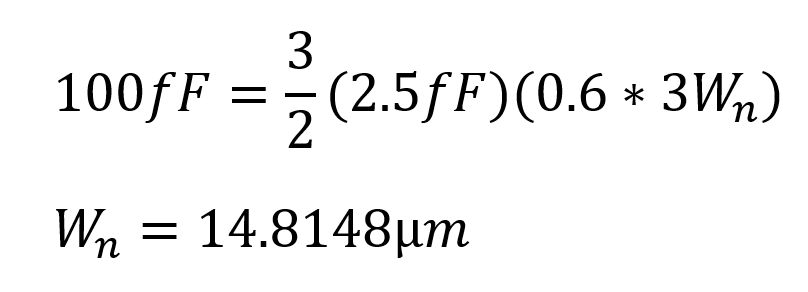
However, we don’t want
to be on that edge since going over is a failure state so let’s shoot for 90%
of our targeted 100fF input capacitance.
Now knowing the
constraints on the grid and that to add even more cushion I’m going to round
down to use a 26.1/13.05 inverter so that on the layout I can use 8.7µ m=3 and 4.35µ m=3.
Simulatons:
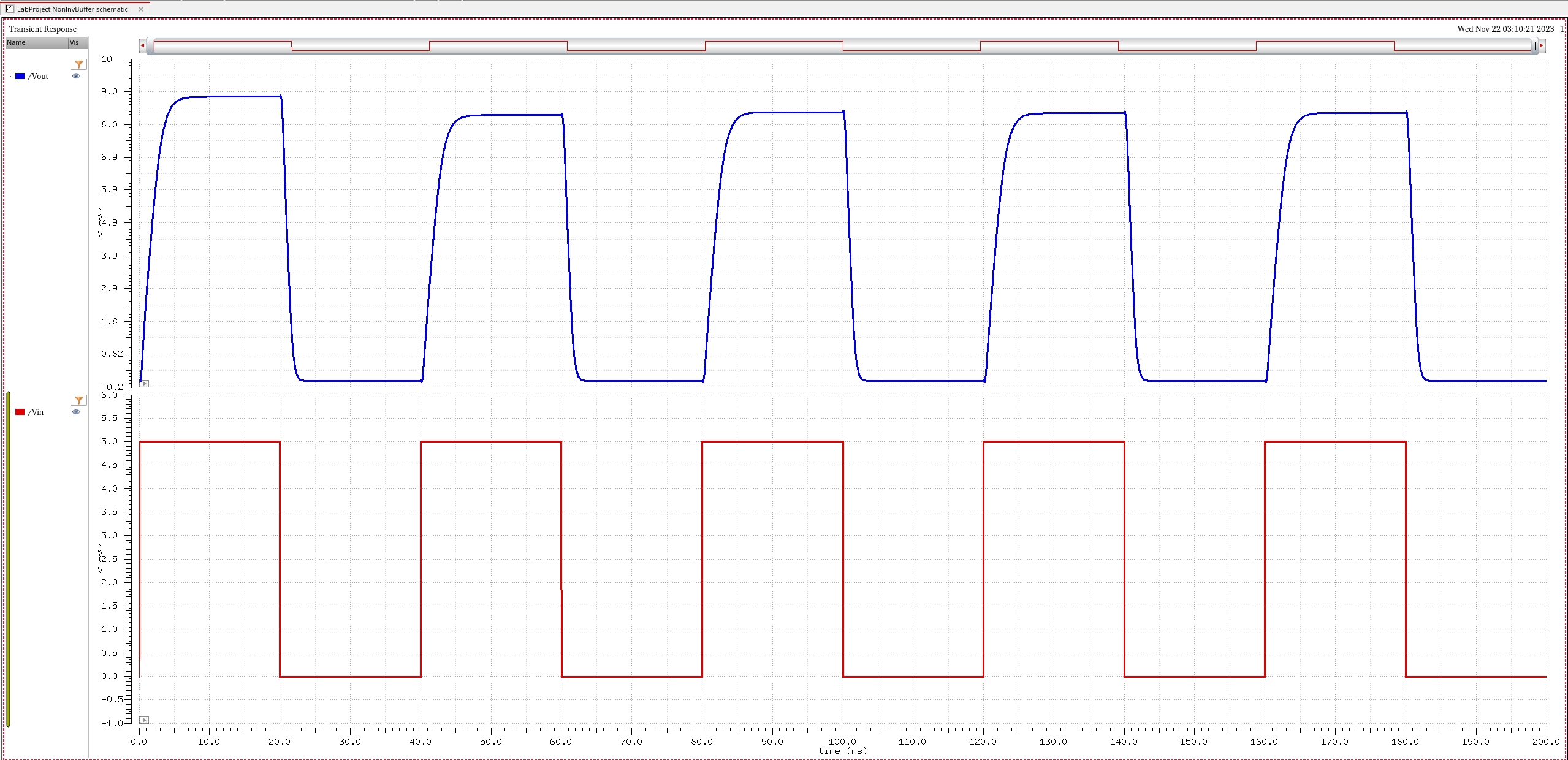
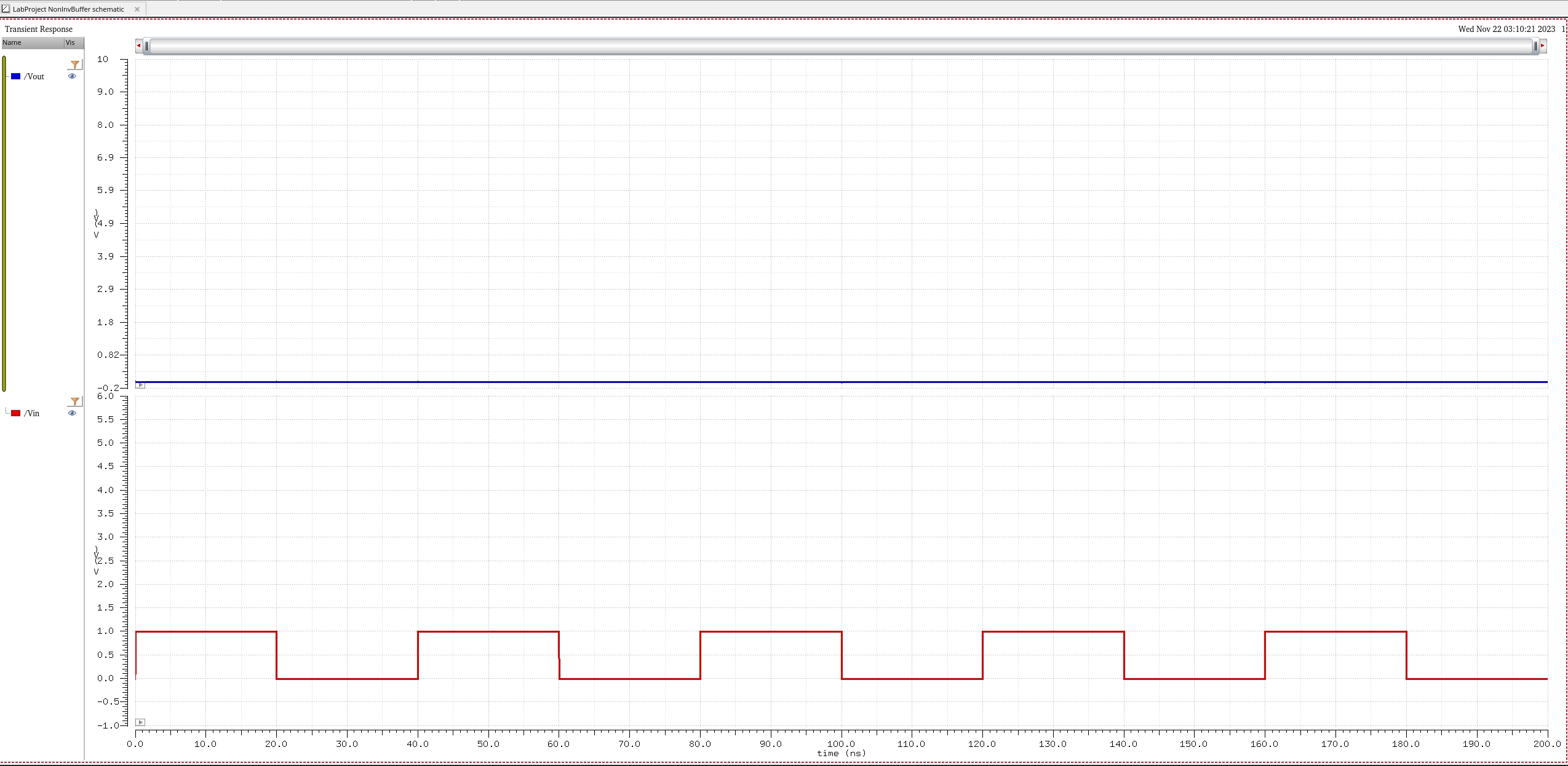
VDD 5V Vin 3V 1pF
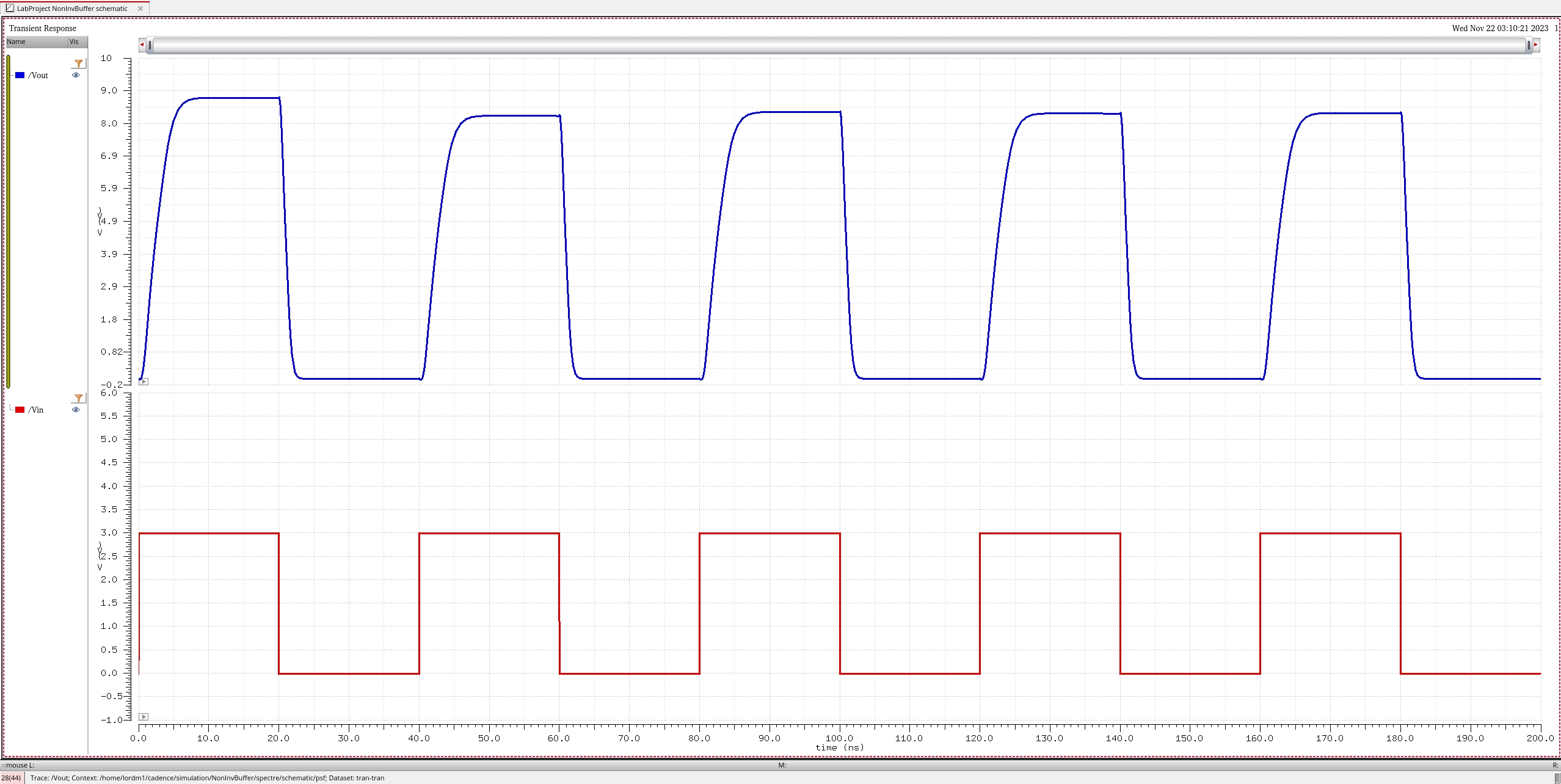
VDD 5V Vin 1V 1pF