Lab 7 - ECE 421L
Lab description
·
In this lab, we will use buses and arrays to design word
inverters, muxes, and high-speed adders.
Pre-Lab
Going Through Tutorial 5
·
In its entirety, tutorial 5 takes us through:
o Introduction
to instance arrays
o Schematic of
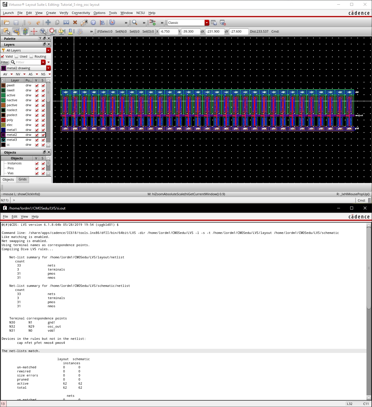
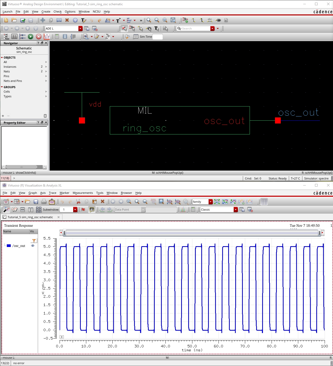
Ring Oscillator (31 inverters)
o Simulation of
Ring Oscillator
o Layout of Ring Oscillator
Shown here are my completed schematic and layout of the Ring Oscillator.
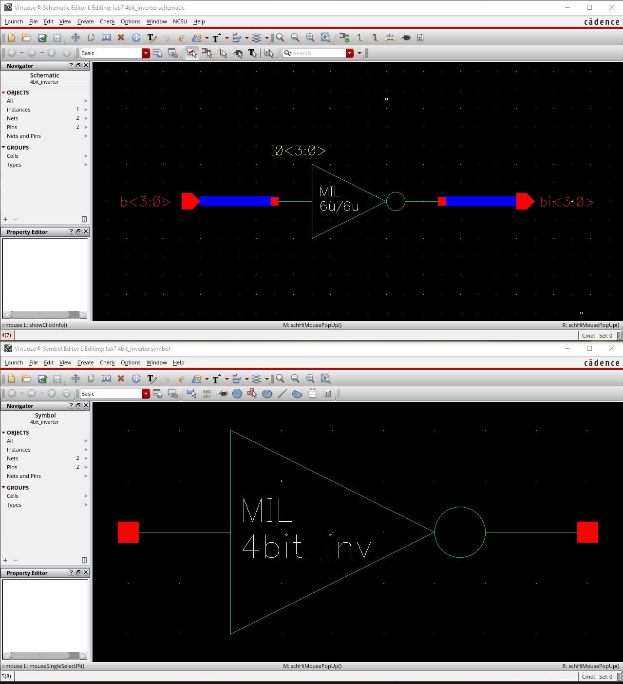
Create the array of four
inverters and simulate it.
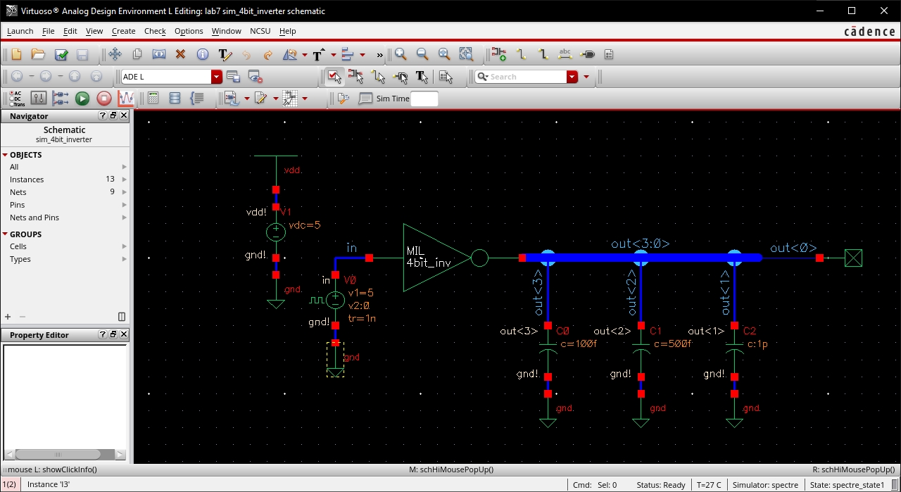
Show, in your lab report,
how a capacitive load influences the delay and rise/fall times.
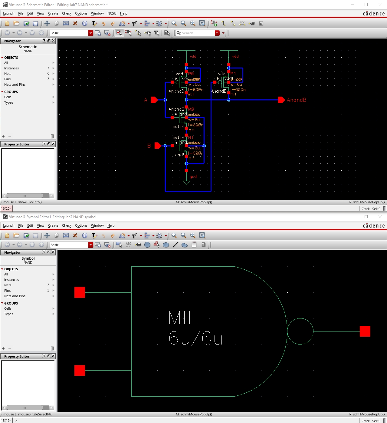
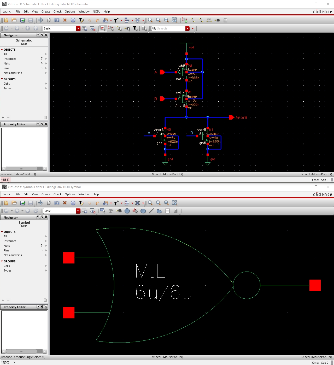
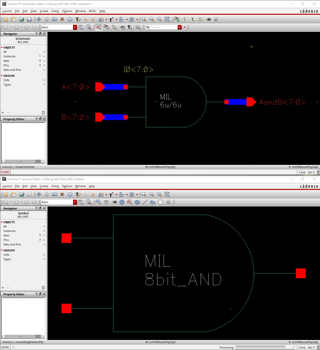
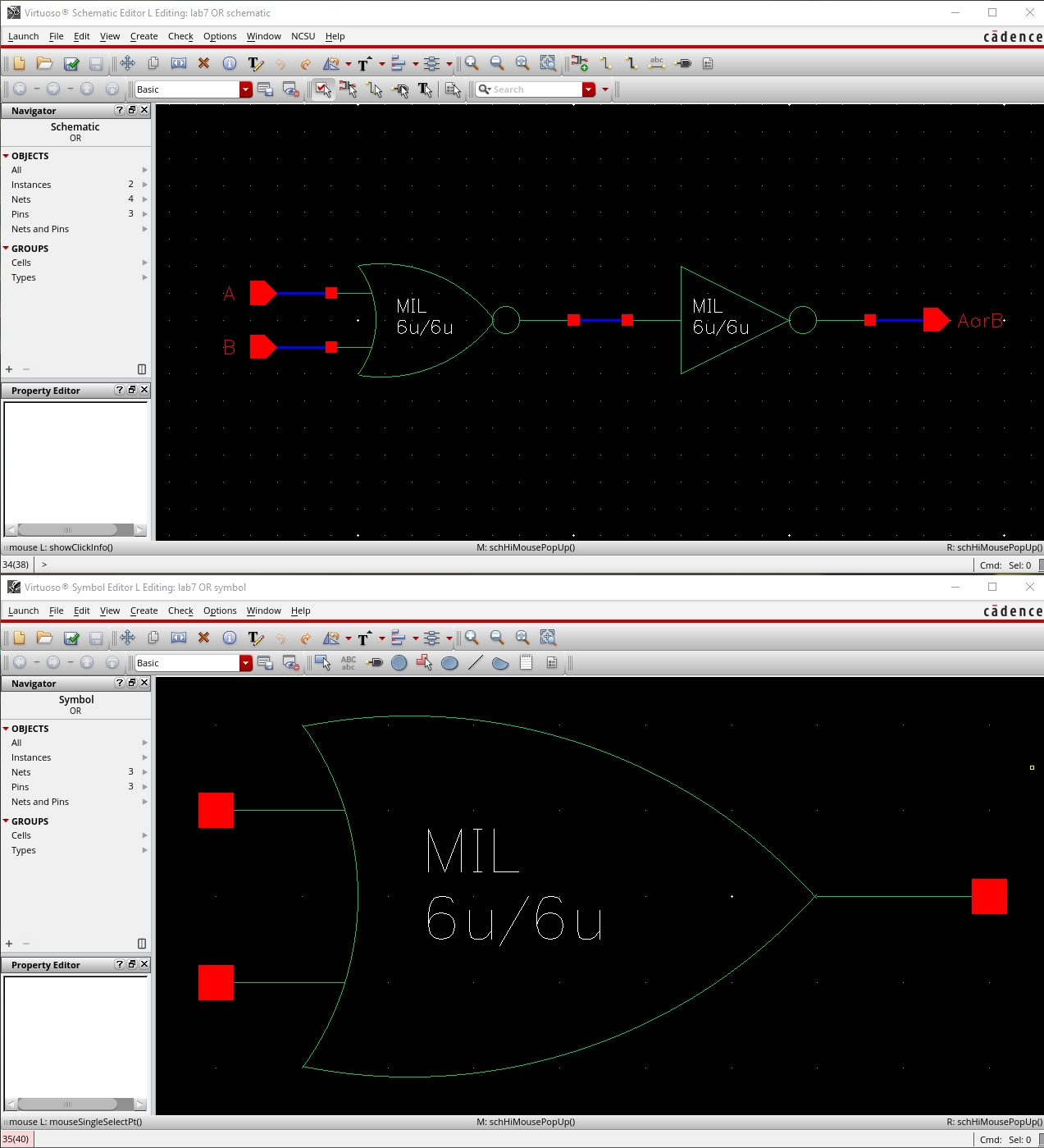
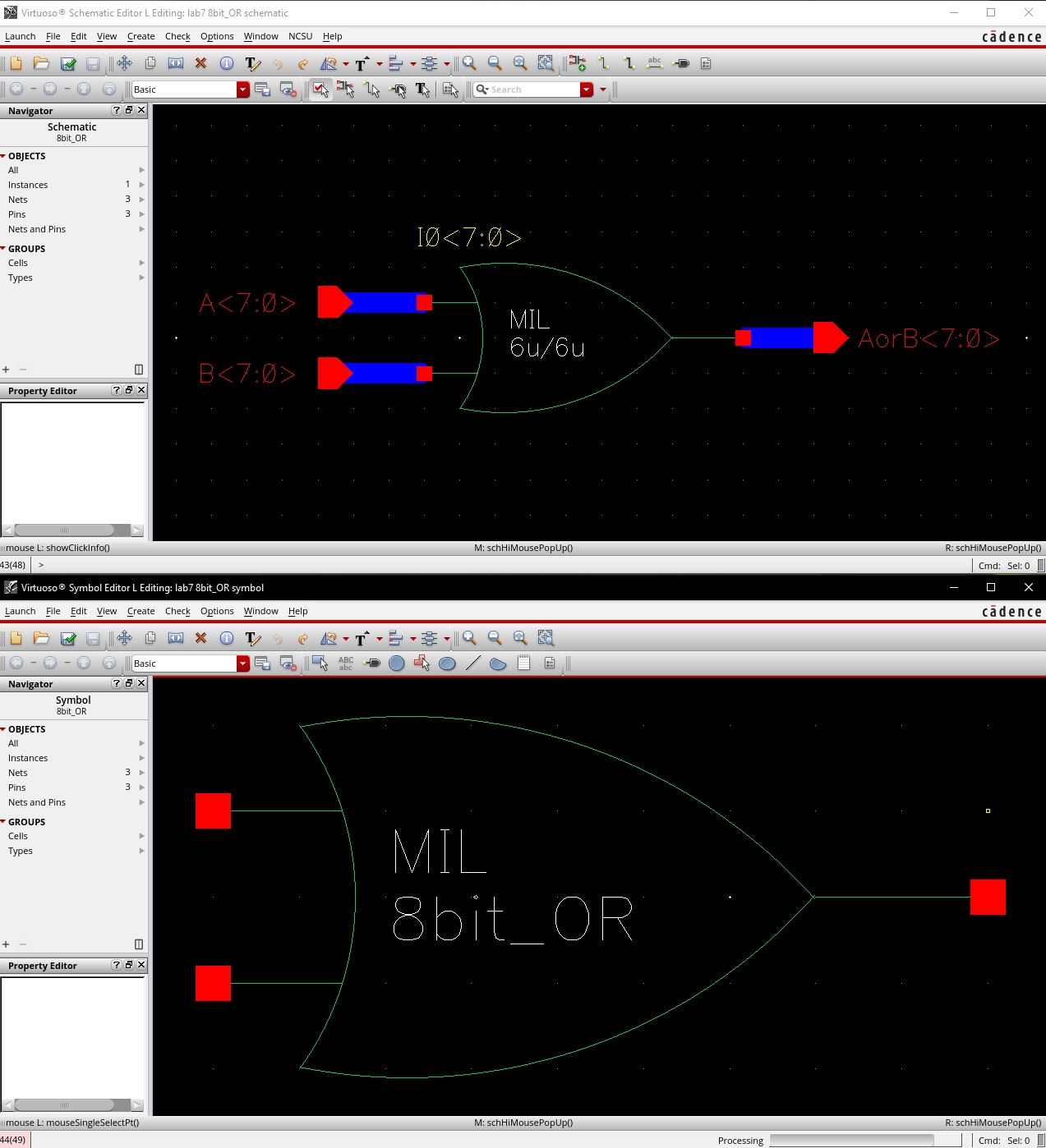
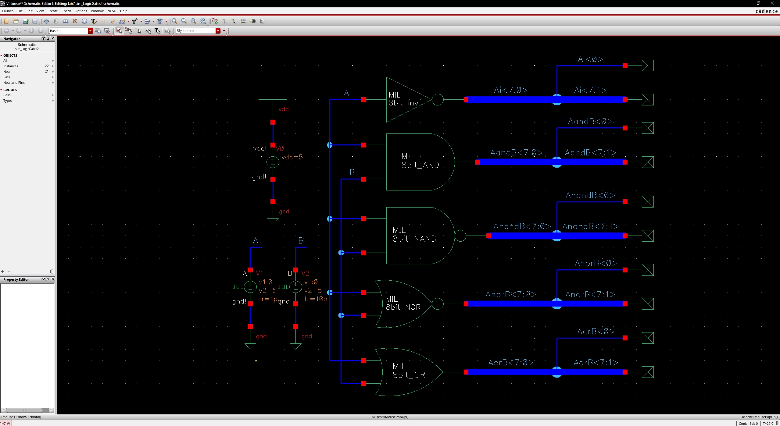
Create
schematics and symbols for an 8-bit input/output array of: NAND, NOR, AND,
inverter, and OR gates.
Provide a few simulation examples using these
gates.
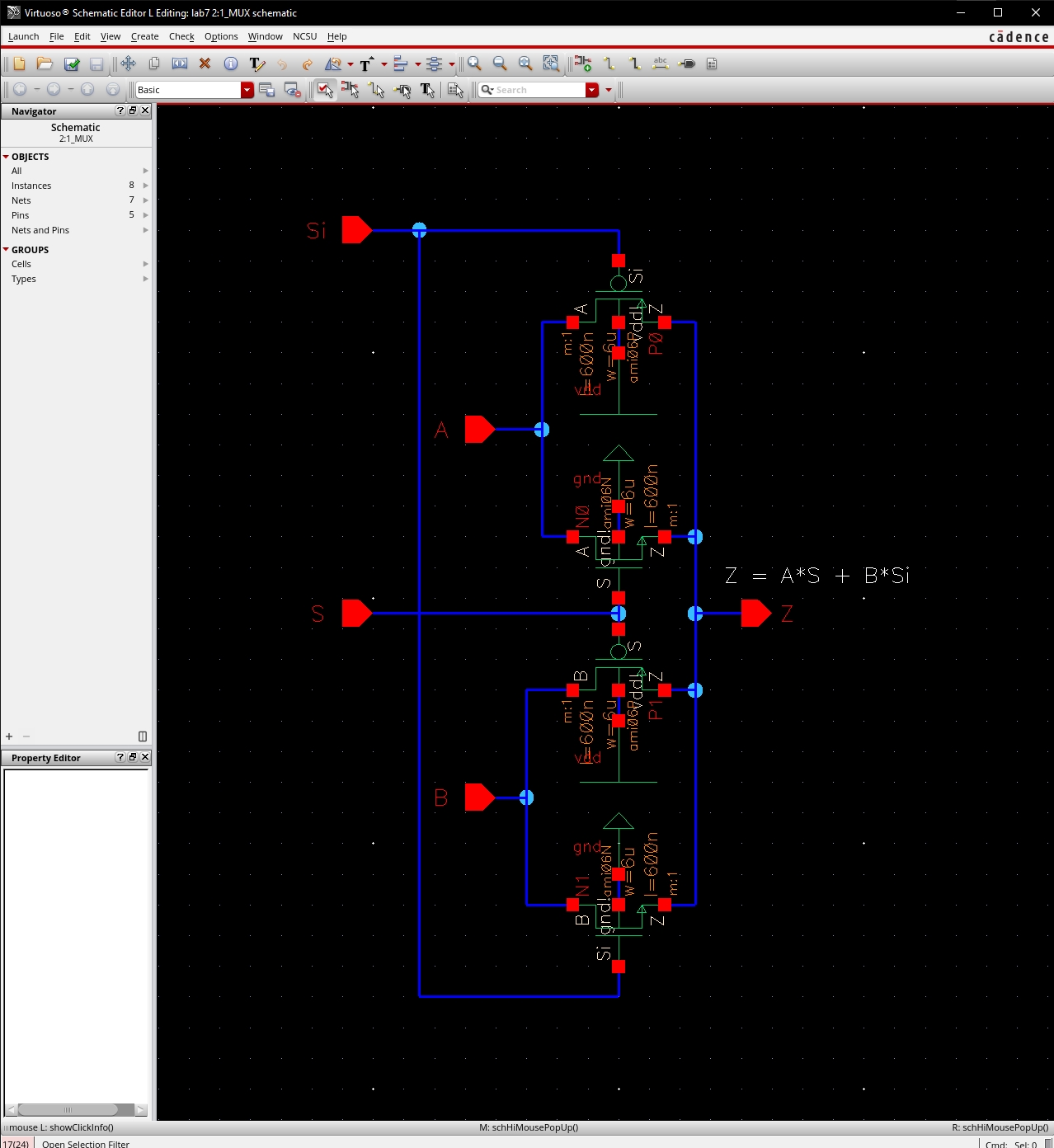
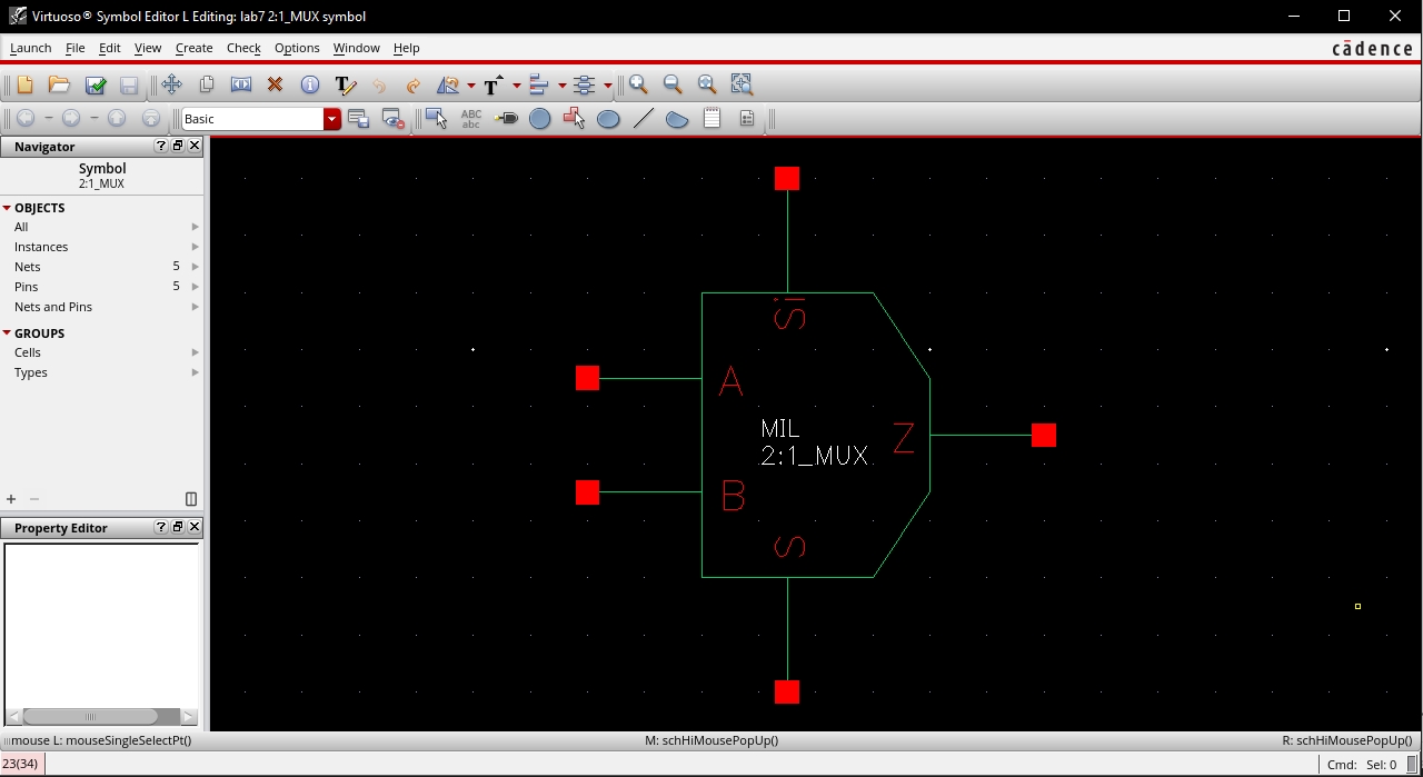
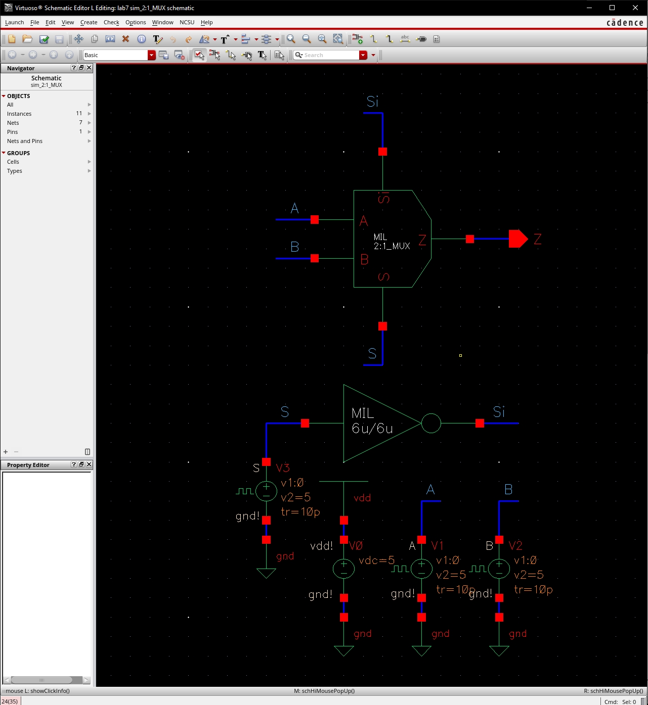
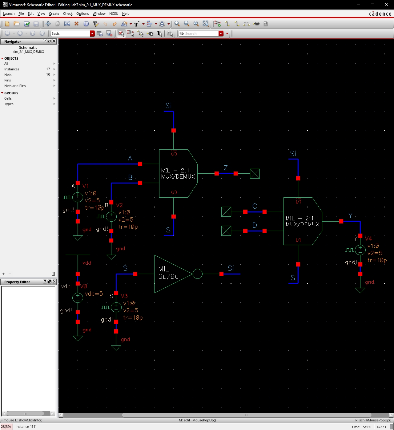
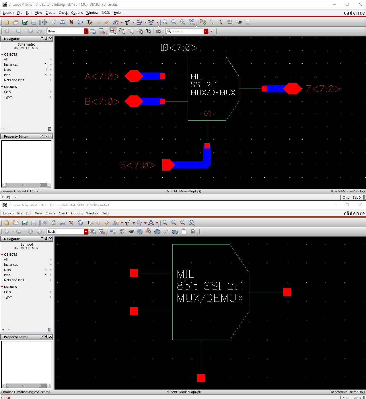
Create an
8-bit wide word 2-to-1 DEMUX/MUX schematic and symbol.
Include an inverter in your design so the cell
only needs one select input, S (the complement, Si, is generated using an
inverter).
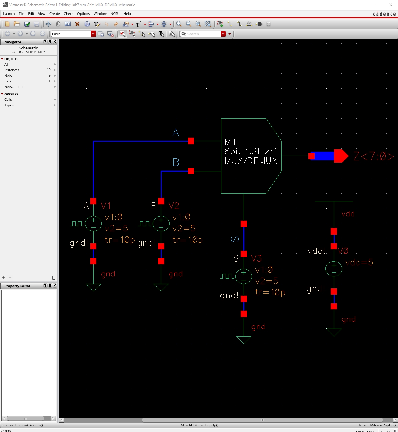
Use simulations to verify the operation of
your design.
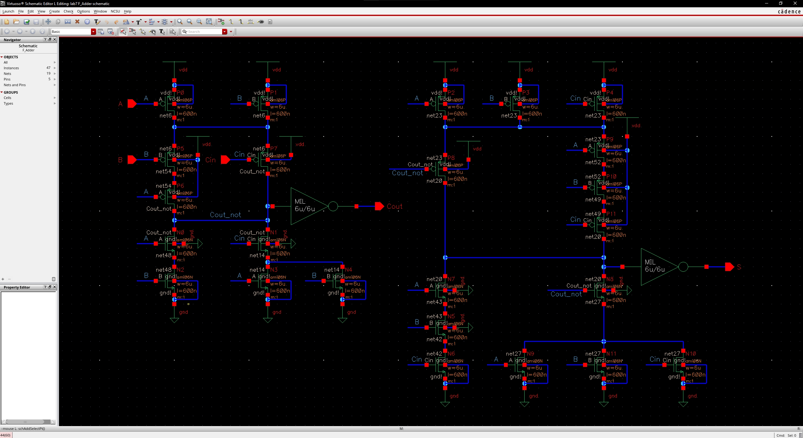
Finally, draft the schematic of the full-adder
seen in Fig. 12.20 using 6u/0.6u devices (both PMOS and NMOS).
Create an adder symbol for this circuit (see
the symbol used in lab6).
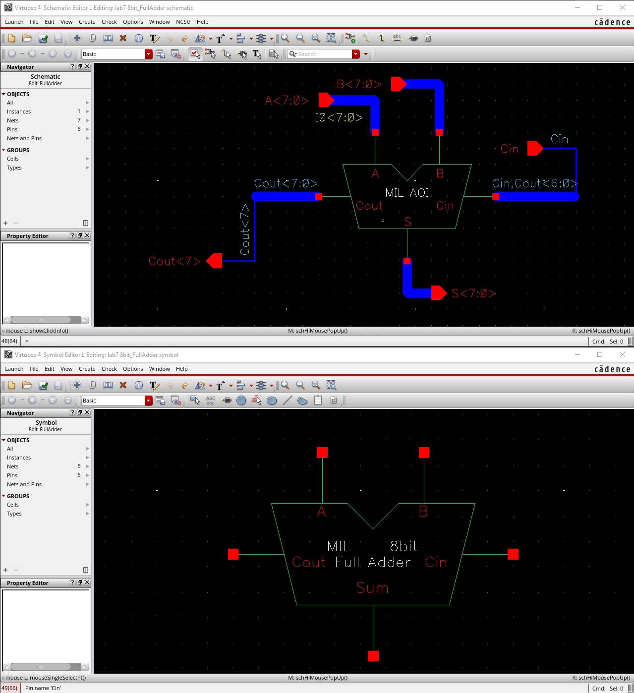
Use this symbol to draft an 8-bit adder
schematic and symbol.
For how to label the bus so the carry out of
one full-adder goes to the carry in of another full-adder review the ring
oscillator schematic discussed in Cadence Tutorial 5.
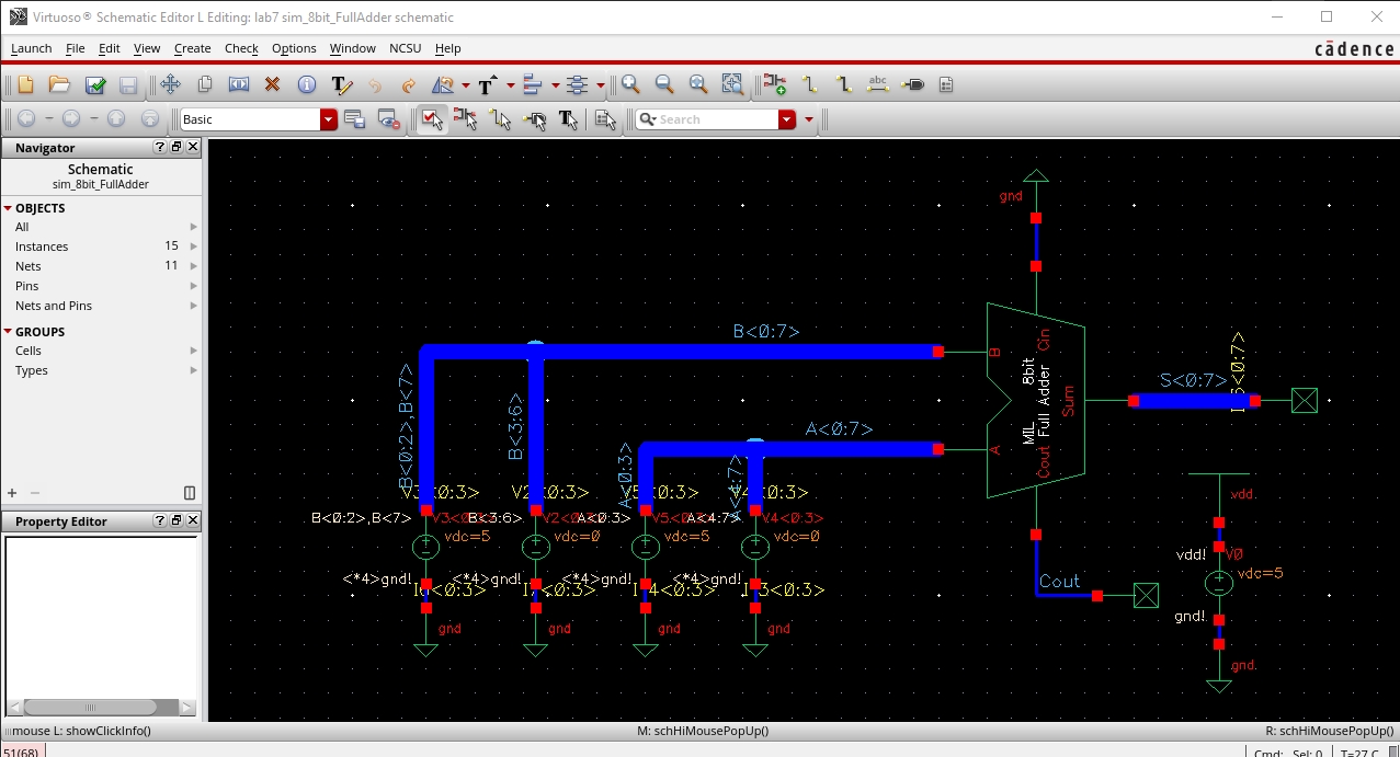
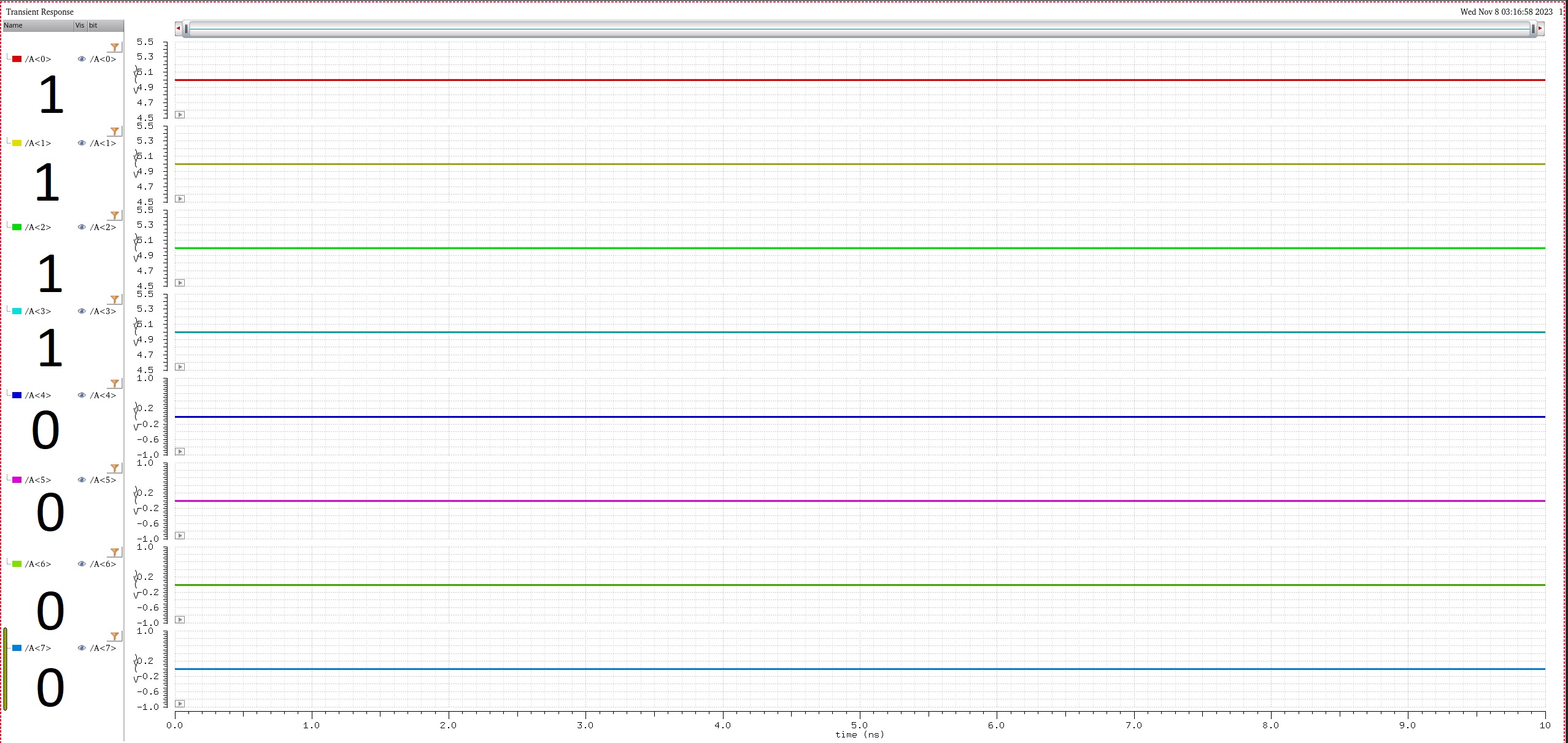
Simulate the operation of your 8-bit adder.
Lay out this 8-bit adder cell (*note* that
this is the only layout required in this lab).
Show that your layout DRCs and LVSs
correctly.
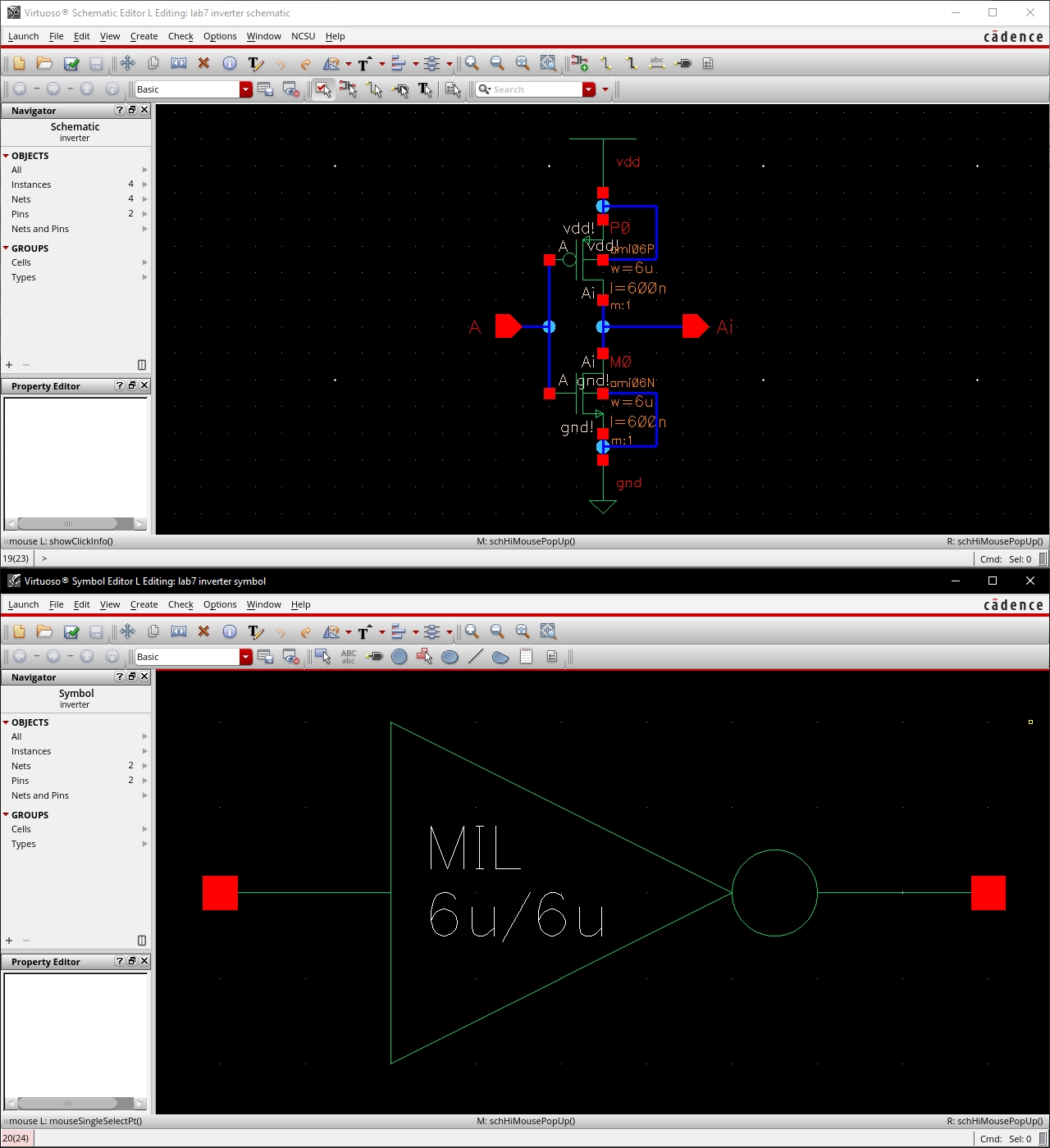
4-bit Inverter
Schematic and Symbol
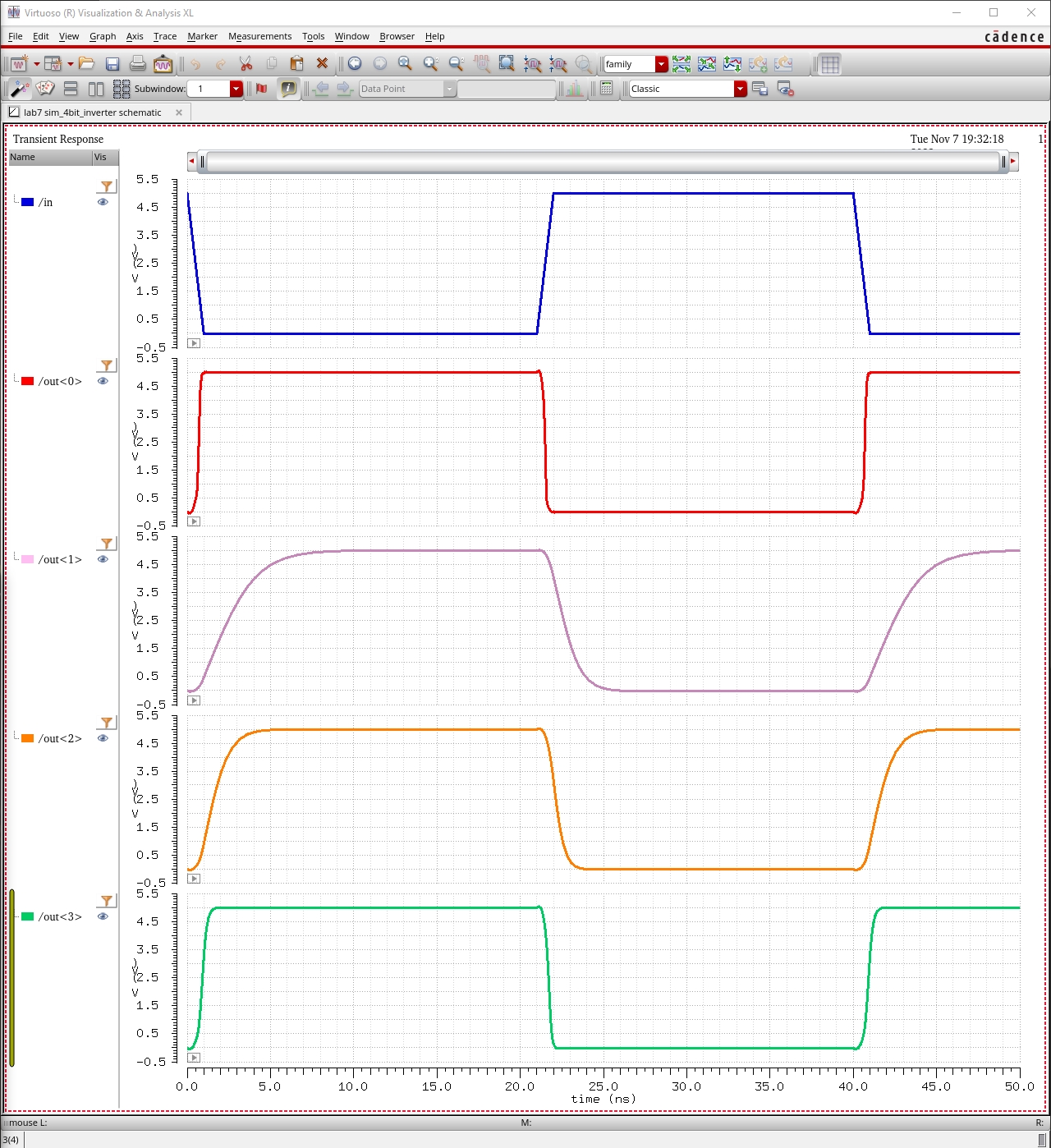
4-bit Inverter
Simulation Results
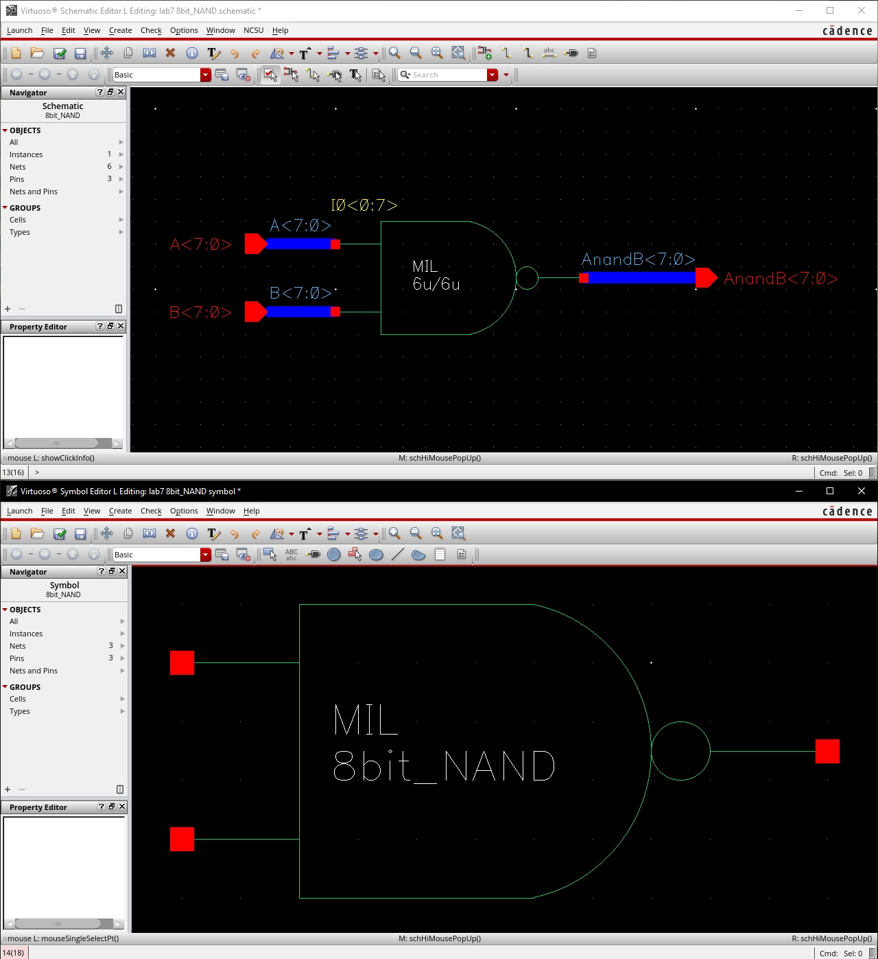
For each of
the following gates, I have included four pictures:
·
The schematic of the gate
·
The symbol of the gate
·
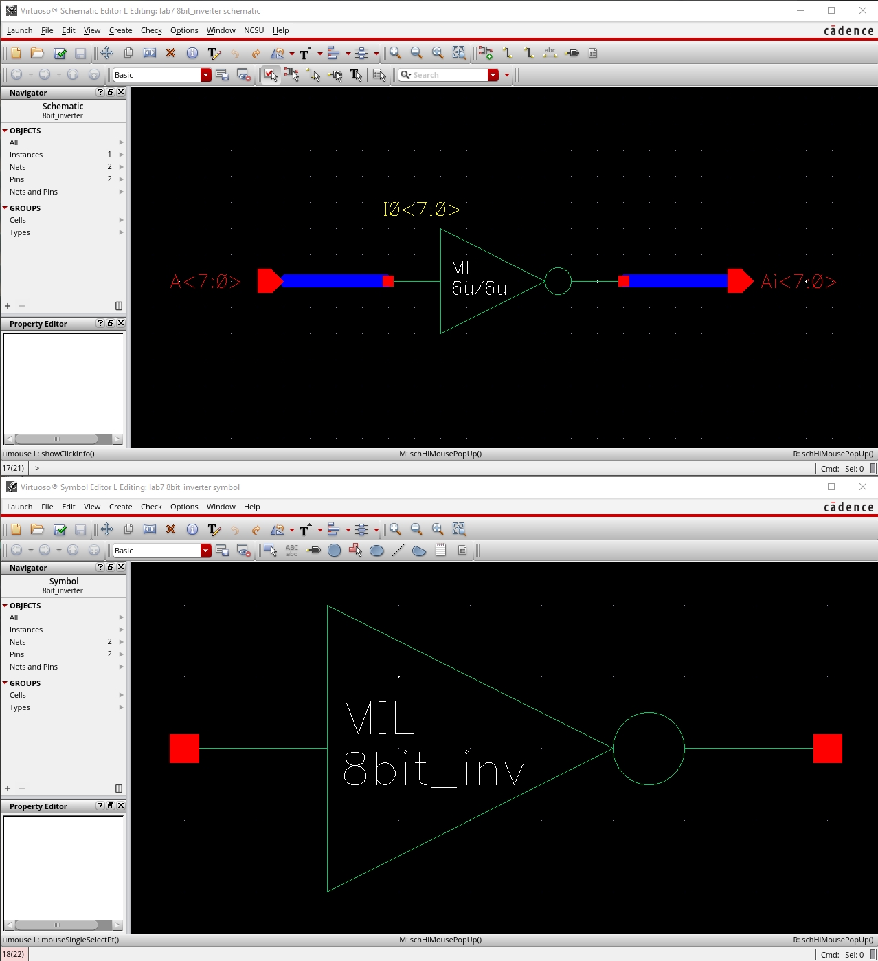
The schematic of the 8-bit gate
·
The symbol of the 8-bit gate
8-Bit I/O Array of NOT Gate
8-Bit I/O Array of NOR Gate
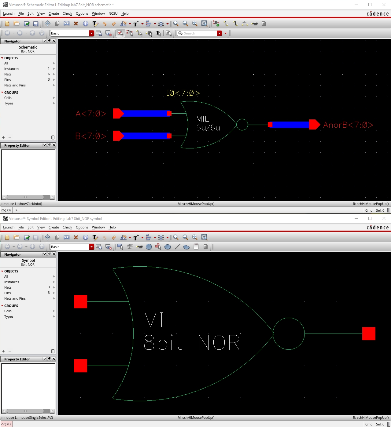
8-Bit I/O Array of AND Gate
·
To simulate the gates, I had A & B square wave inputs act as the truth table inputs for the gates.
o The LSB <0> of each
of the gates’ output was branched off and plotted in the simulation.
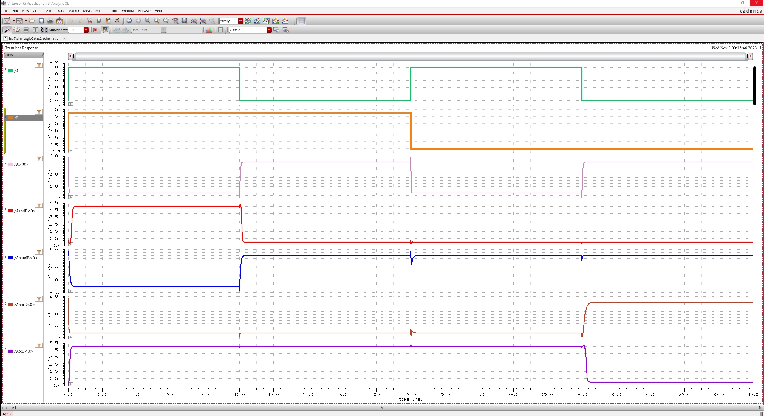
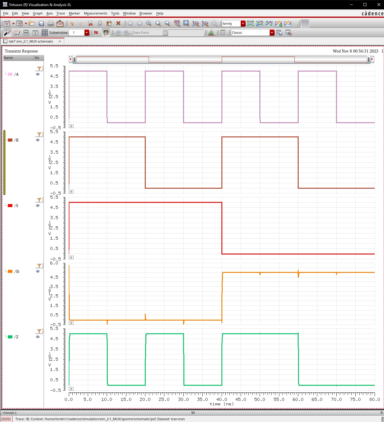
2:1 MUX
Simulation Results of 2:1 MUX
We can observe
from the simulation below that:
·
When S is high, the output Z follows input A.
· When S is low, the output Z follows input B.
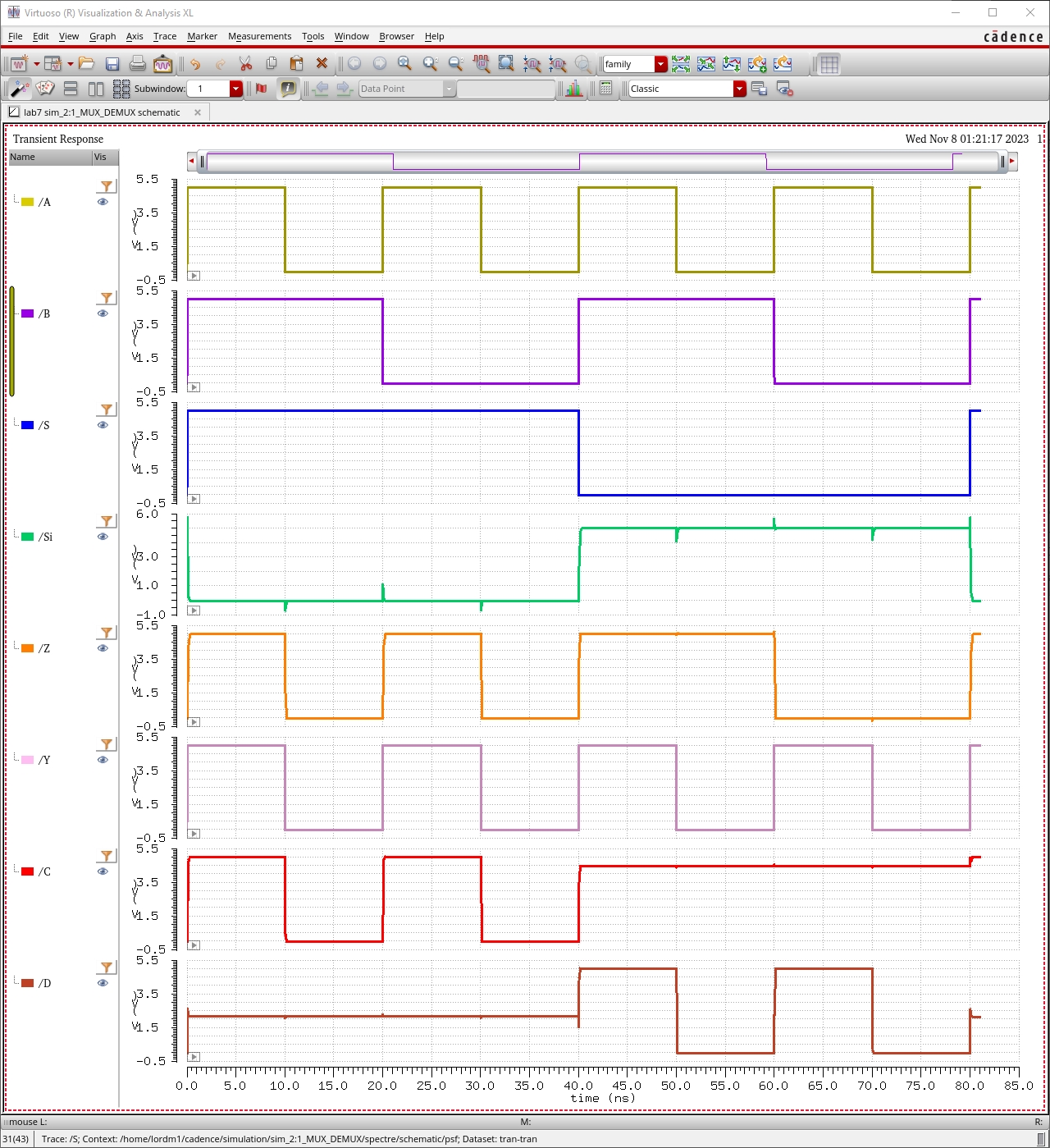
Simulation Results of 2:1 MUX/DEMUX
From the MUX
simulation, we can observe that:
·
When S is high, the output Z follows input A.
·
When S is low, the output Z follows input B.
From the DEMUX
simulation, we can observe that:
·
When S is high, the input signal Y propagates through to C only.
·
When S is low, the input signal Y propagates through to D only.
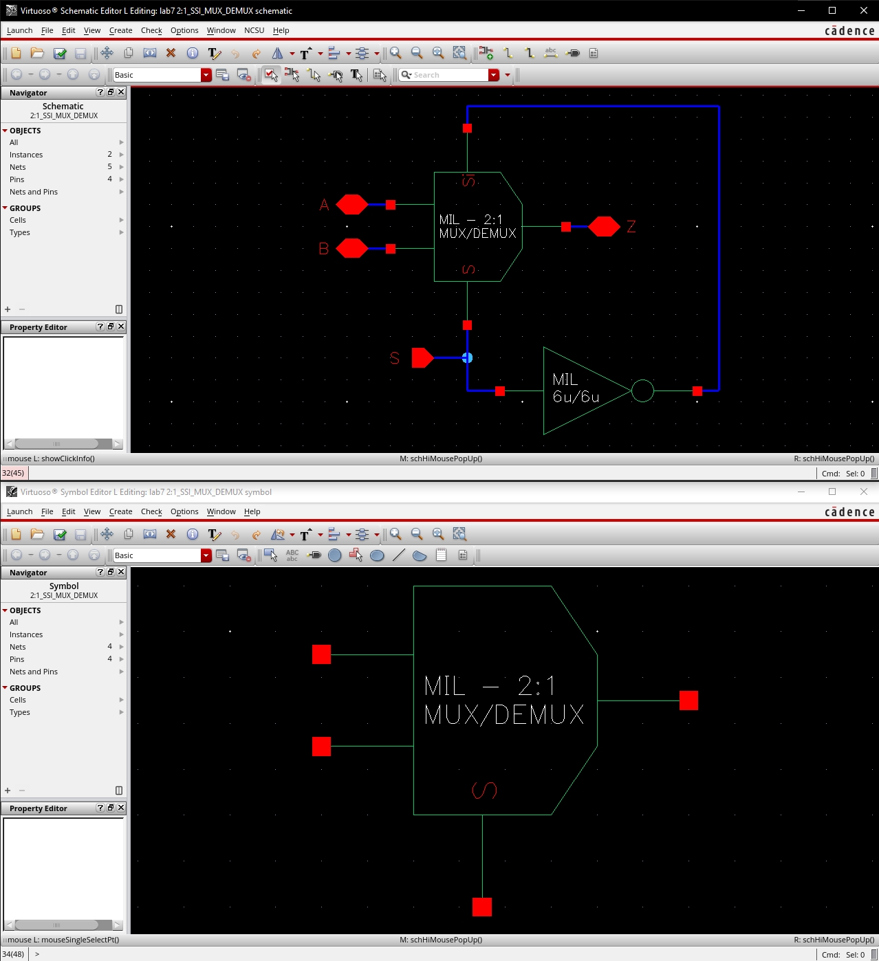
2:1 MUX with Single Select Input
·
Instead of having individual inputs for S and Si, we connect an
inverter to the S input.
·
Tying the output of this inverter to the Si pin allows us to create
a MUX with a single select input.
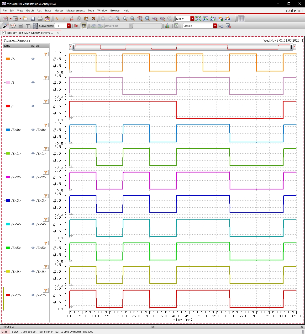
From the 8-bit
MUX simulation below, we see that:
·
When S is high, all 8 bits of output Z follow input signal A.
·
When S is low, all 8 bits of output Z follow input signal B.
AOI Full Adder Schematic
·
Shown below is the AOI implementation of a full adder.
·
The schematic was drafted in Cadence based on figure 12.20 in the CMOS
book.
AOI Full Adder Symbol
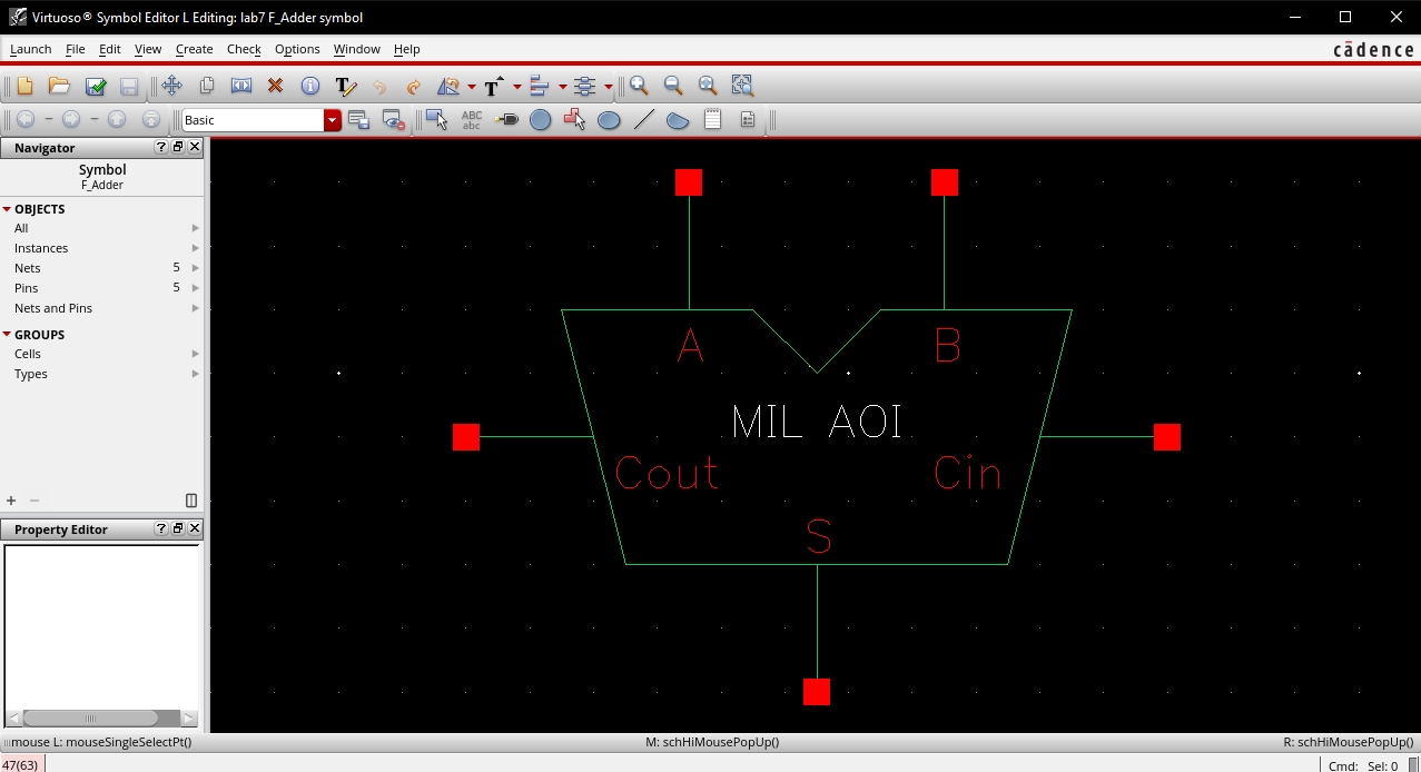
·
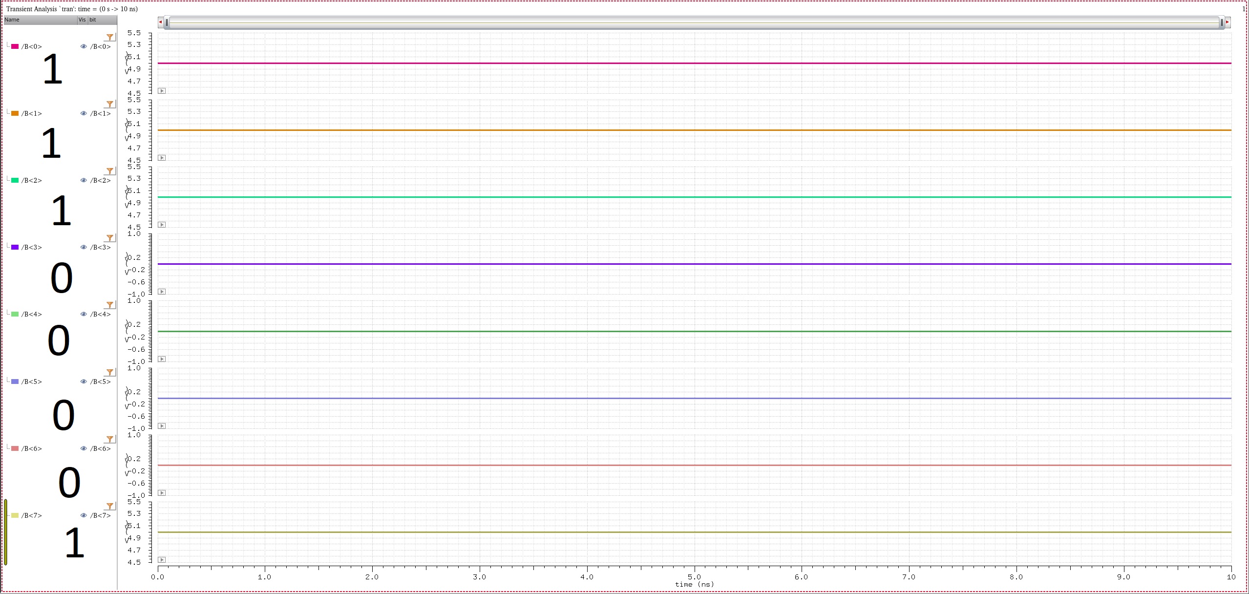
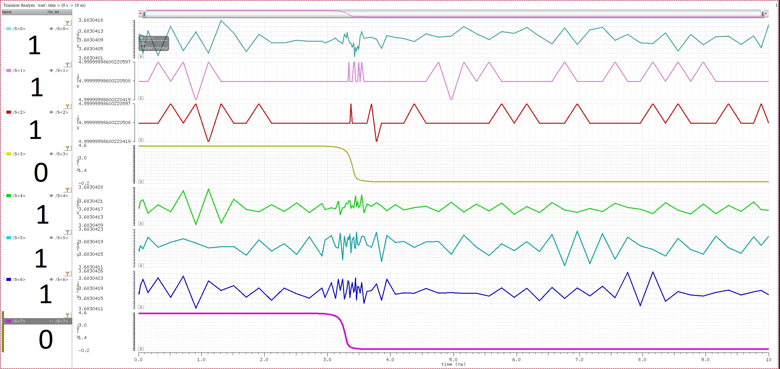
B = 10000111 (binary) = 135 (decimal)
·
A = 00001111 (binary) = 15 (decimal)
·
S = 10010110 (binary) = 150 (decimal)
Its
3:33am and Ive been sick the last week and kinda want to die. I'll be
finishing this later and will talk to you in class about it.