Lab 6 - ECE 421L
Prelab:
Going Through Tutorial 4
·
In its entirety, tutorial 4 takes us through:
o Design of NAND
gate schematic
o Creating
symbol view of NAND gate
o Layout of NAND
gate
o Simulation of
NAND gate schematic
Lab Report:
Lab
Overview:
NAND Gate Construction
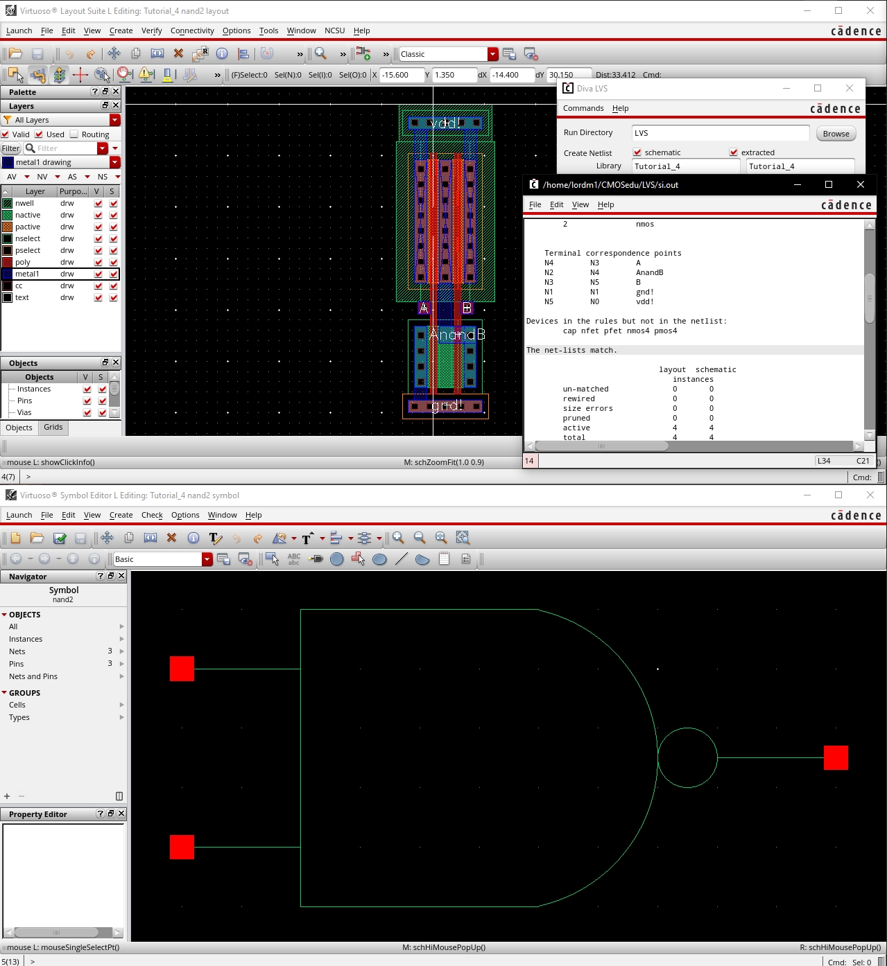
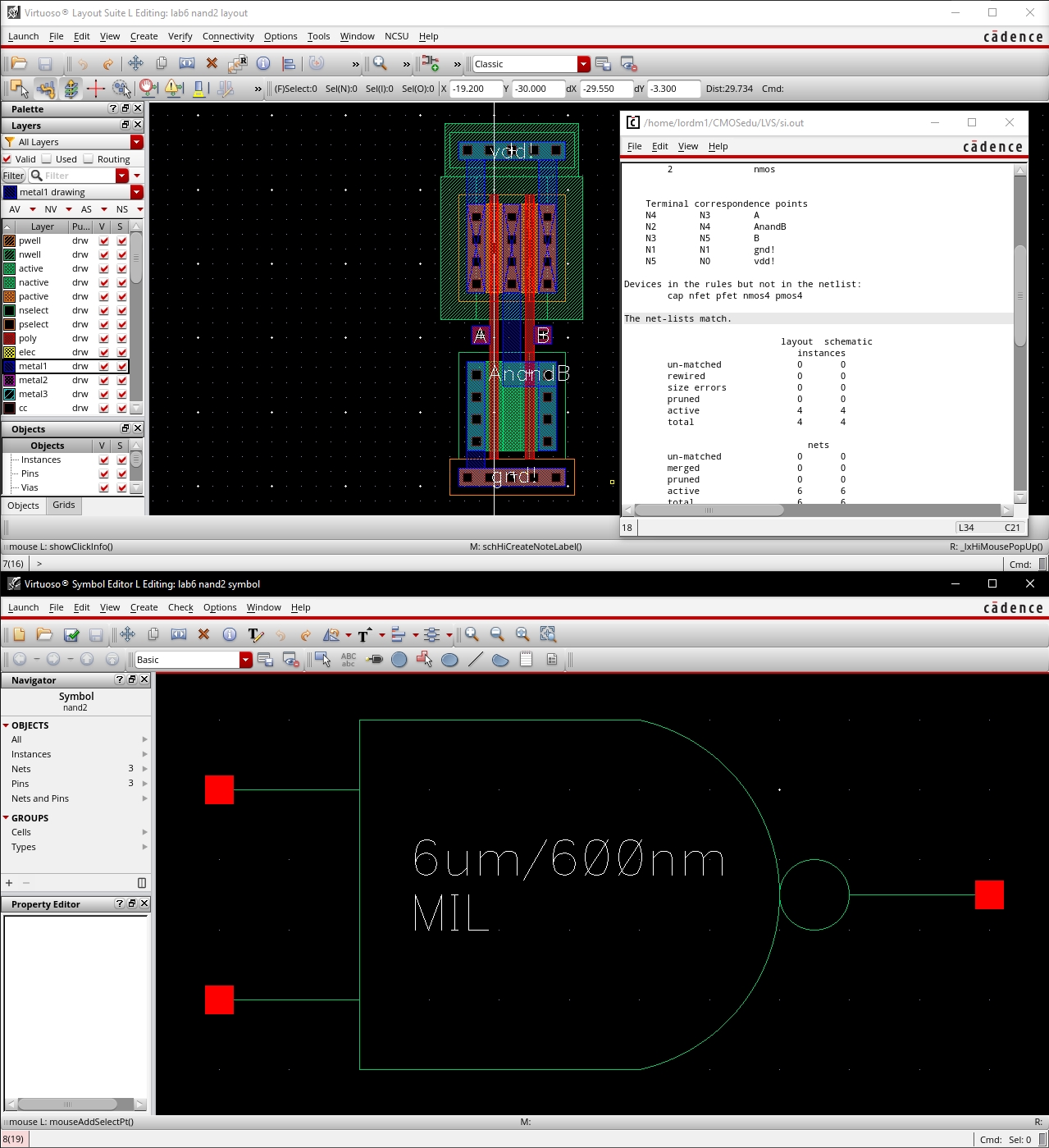
Shown
below are both the layout view of the 2-input NAND gate, consisting of two
NMOS and two PMOS, all of width 6 microns, and length 600 nm, and the symbol
view of the NAND, as well. We see that the layout
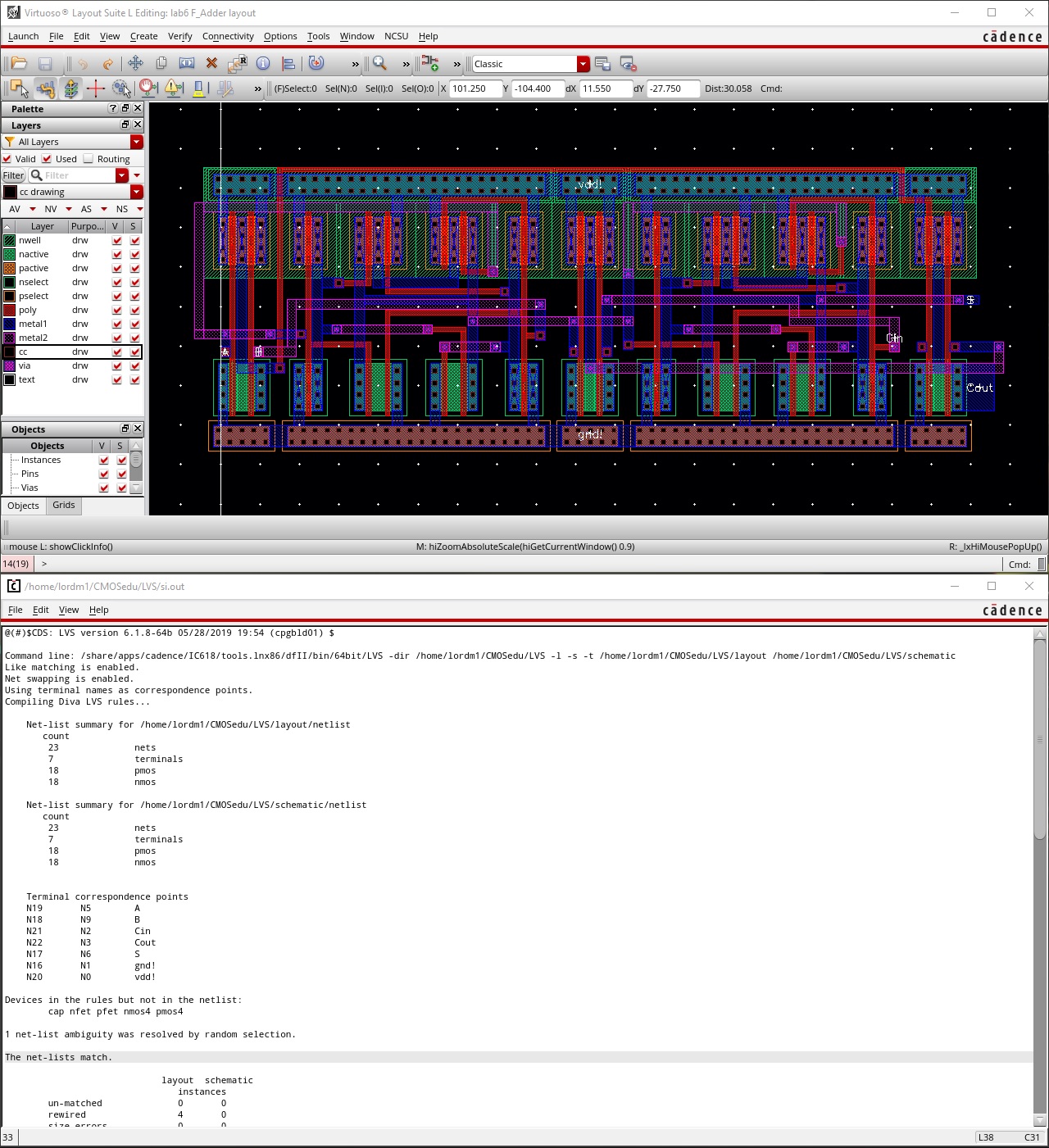
DRC is successful and the LVS shows that the net lists match.
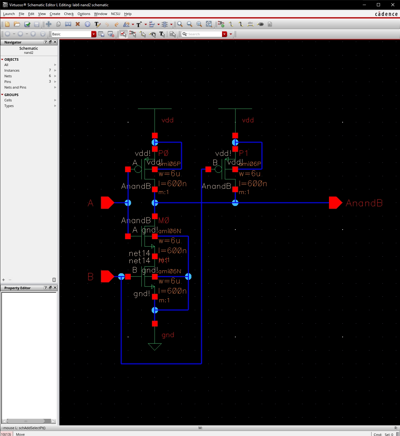
Shown here is the Schematic of the NAND gate.
NAND Gate Simulation Results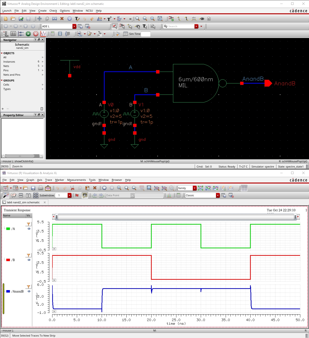
XOR Gate
Construction
Shown
below are both the layout view of the 2-input NAND gate and the symbol
view of the NAND, as well. We see that the layout
DRC is successful and the LVS shows that the net lists match.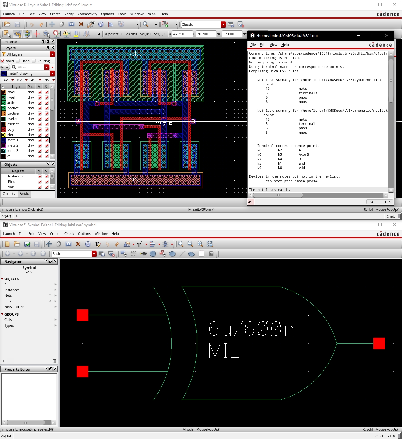
Shown here is the Schematic of the XOR gate.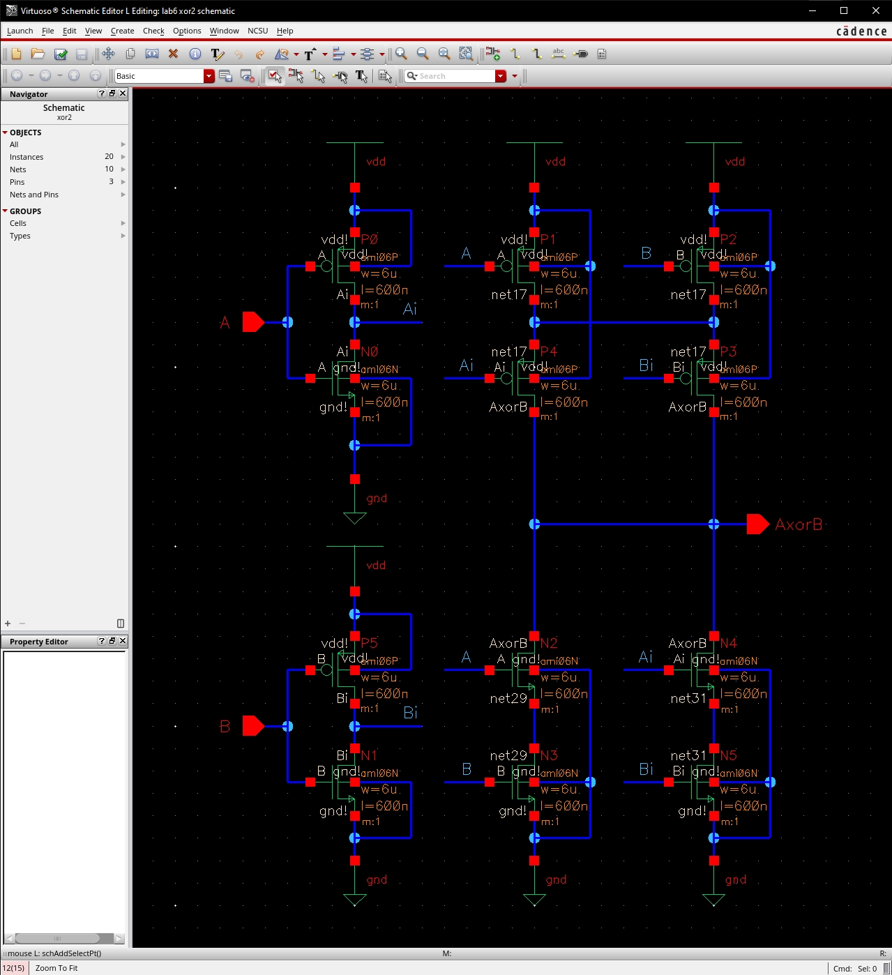
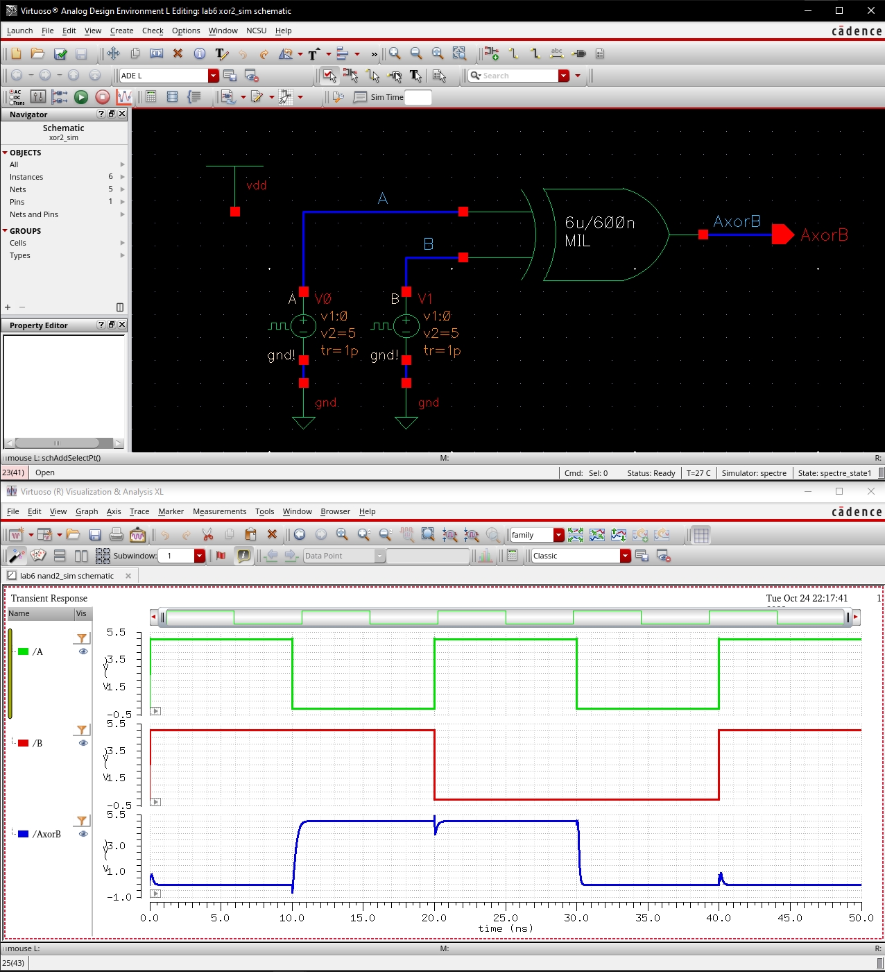
Glitches (NAND and XOR Sims) are caused by the brief rise and fall times of the input signals. The glitch is simply a time period in which the pulse is rising or falling, and the MOSFETs are neither on, nor off. If the rise/fall times could be further decreased as close to instantaneous as possible, the glitches would become smaller and smaller. An ideal rise/fall time of 0 would result in no glitch.
Full Adder
Schematic and Symbol View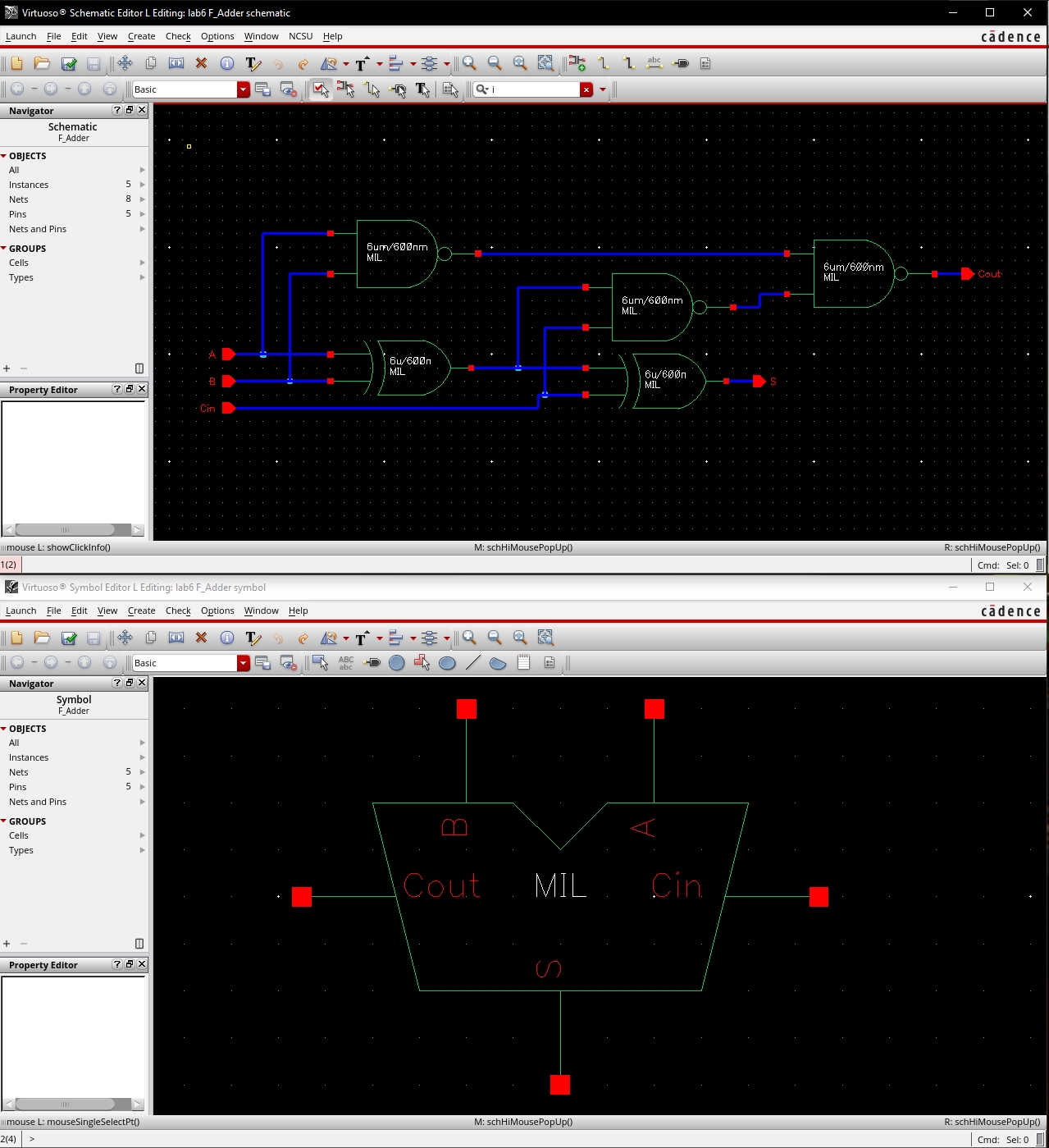
Full Adder
Simulation Results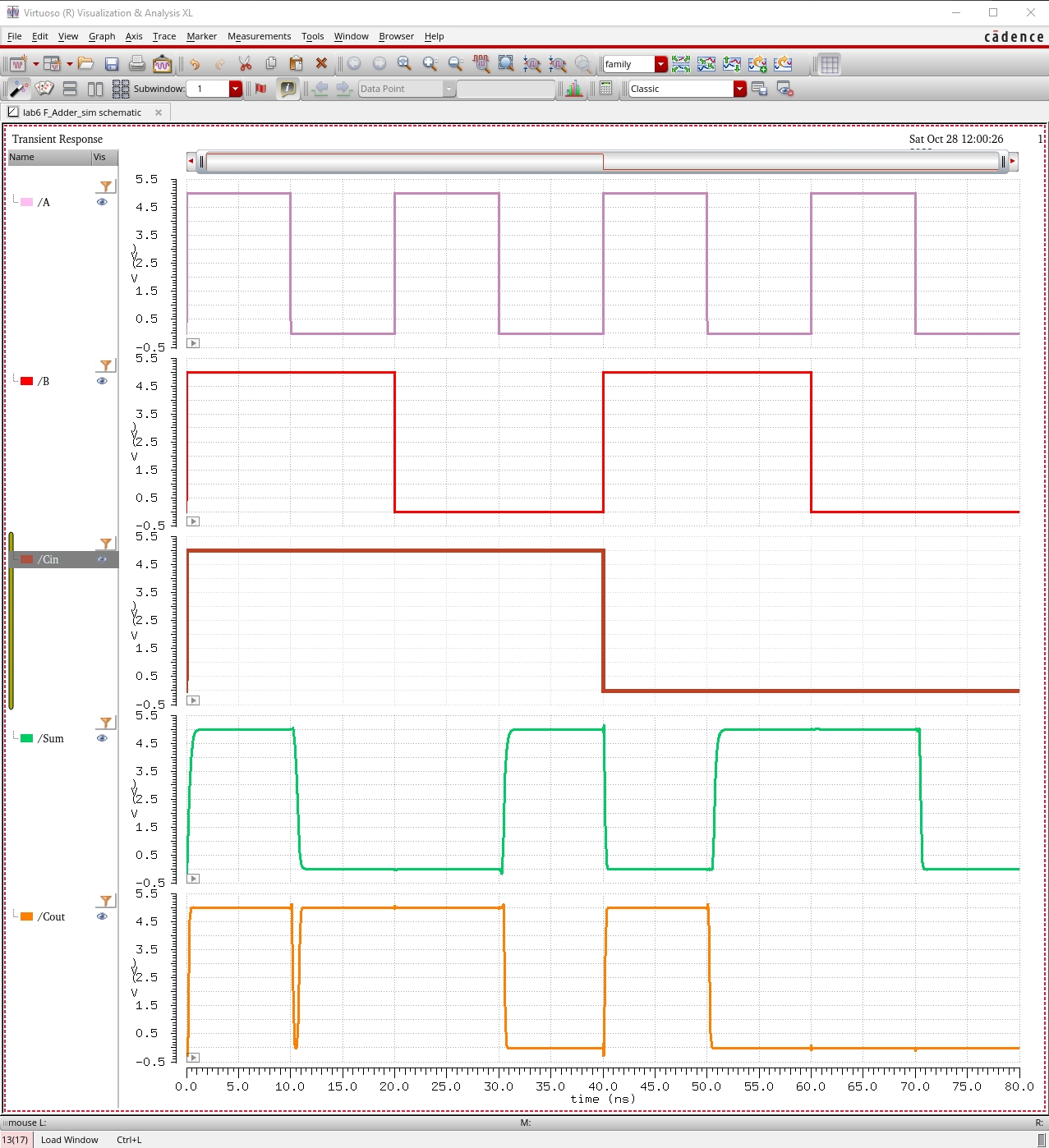
As my last step I ensured my backup to my cloud drive is completed by the green check on the folder and its subfolders incase anything ever goes wrong.
I
use a RAID 1 config on my main computer with the important files being
backed up to my cloud, along with a second computer in my livingroom
that downloads any changes to my files in the cloud, so all in
all I have 2 physical locations using RAID 1 along with my cloud
backup.