Lab 5 - ECE 421L
Prelab:
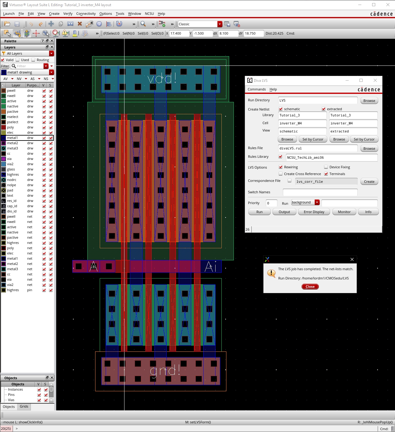
Going Through Tutorial 3
o Simulation of inverter schematic
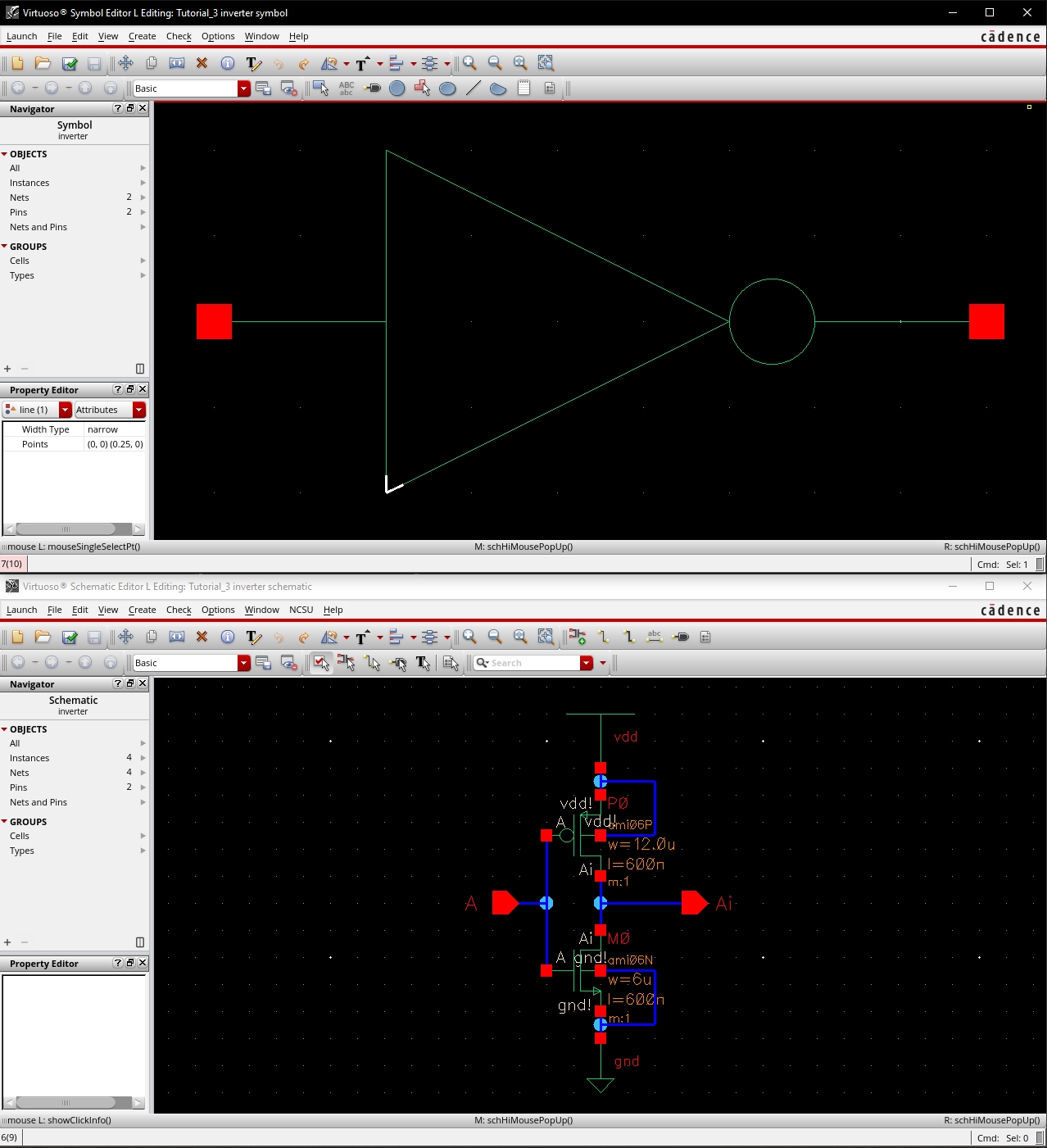
Below is my symbol and schematic for tutorial 3.
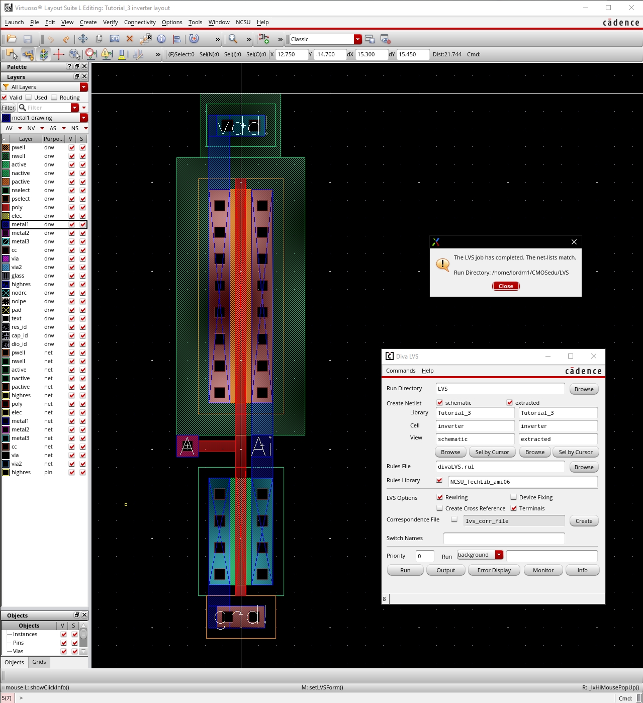
Here is my Layout showing a good LVS for tutorial 3.
Lab Report:
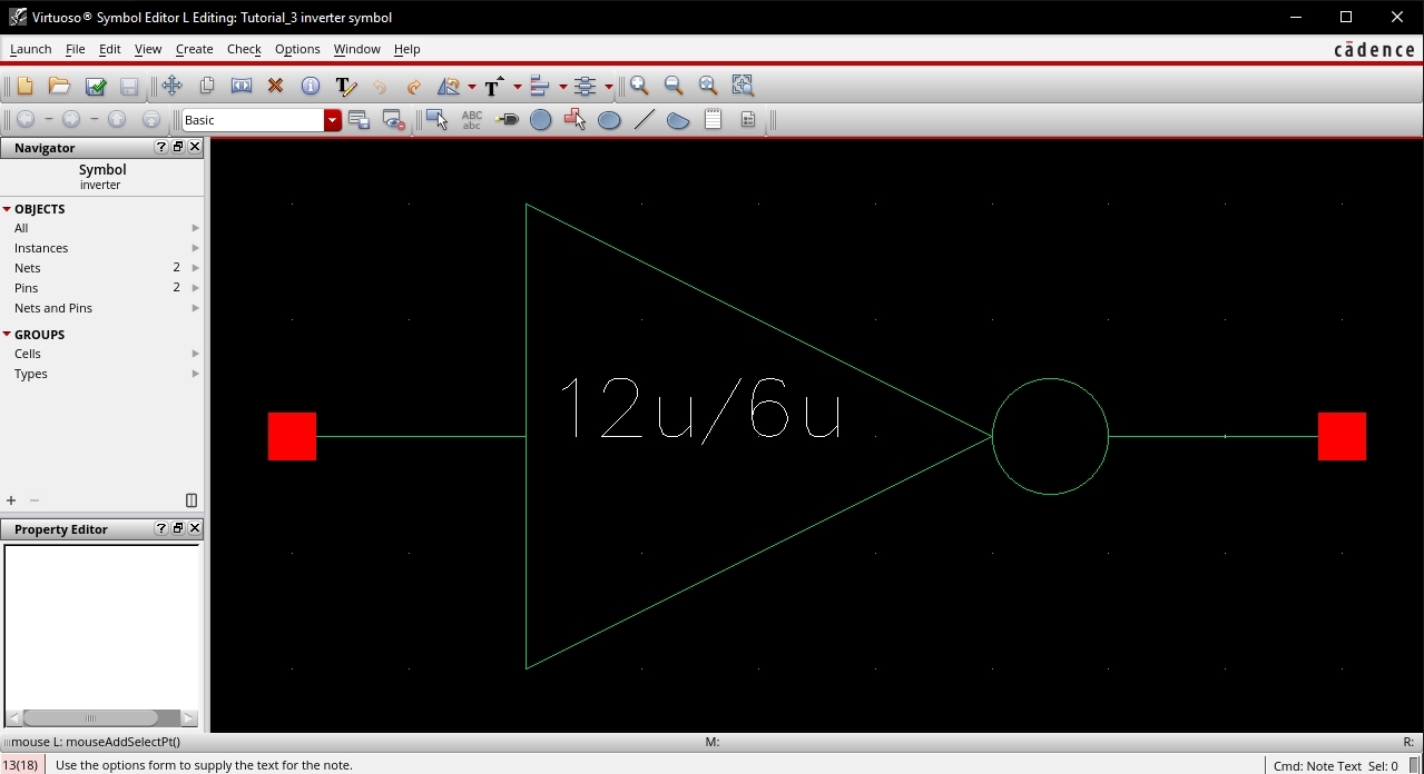
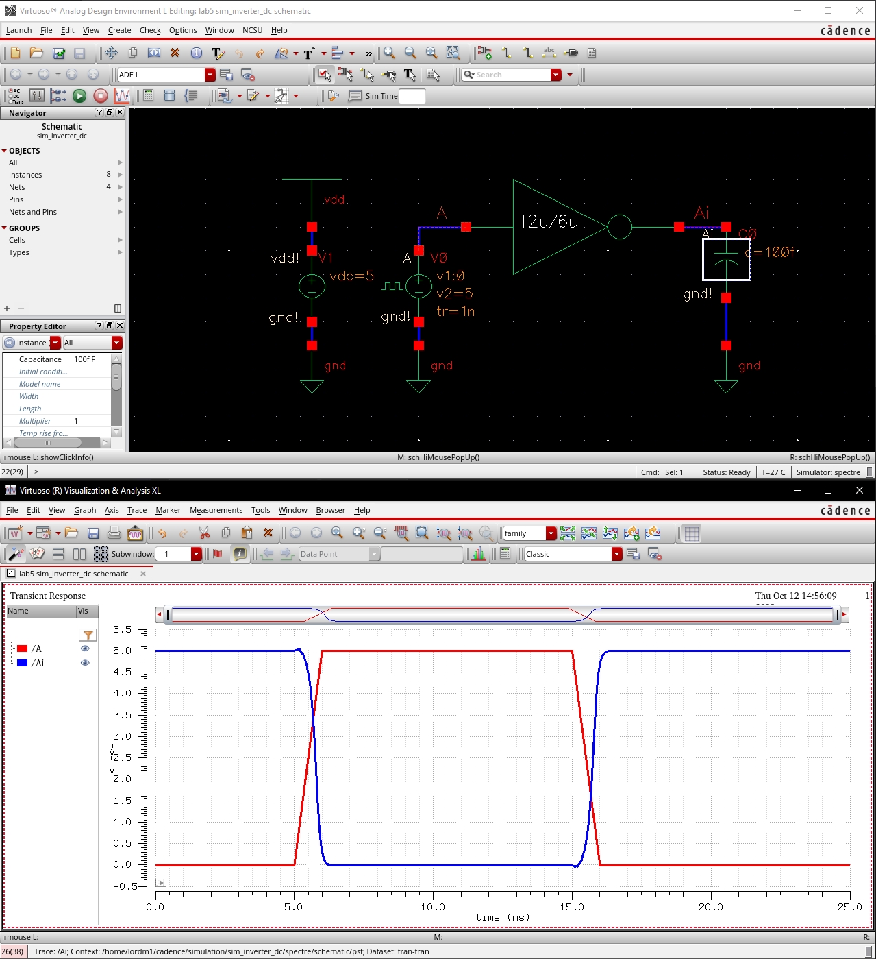
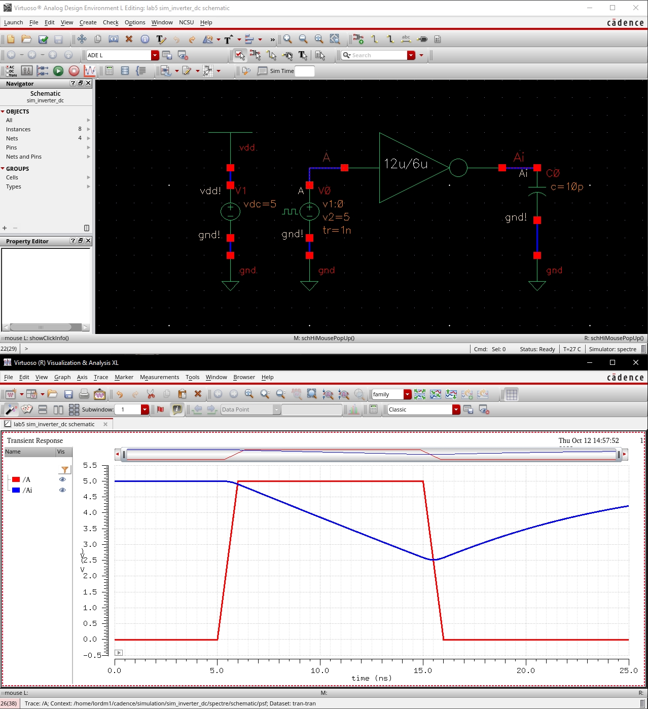
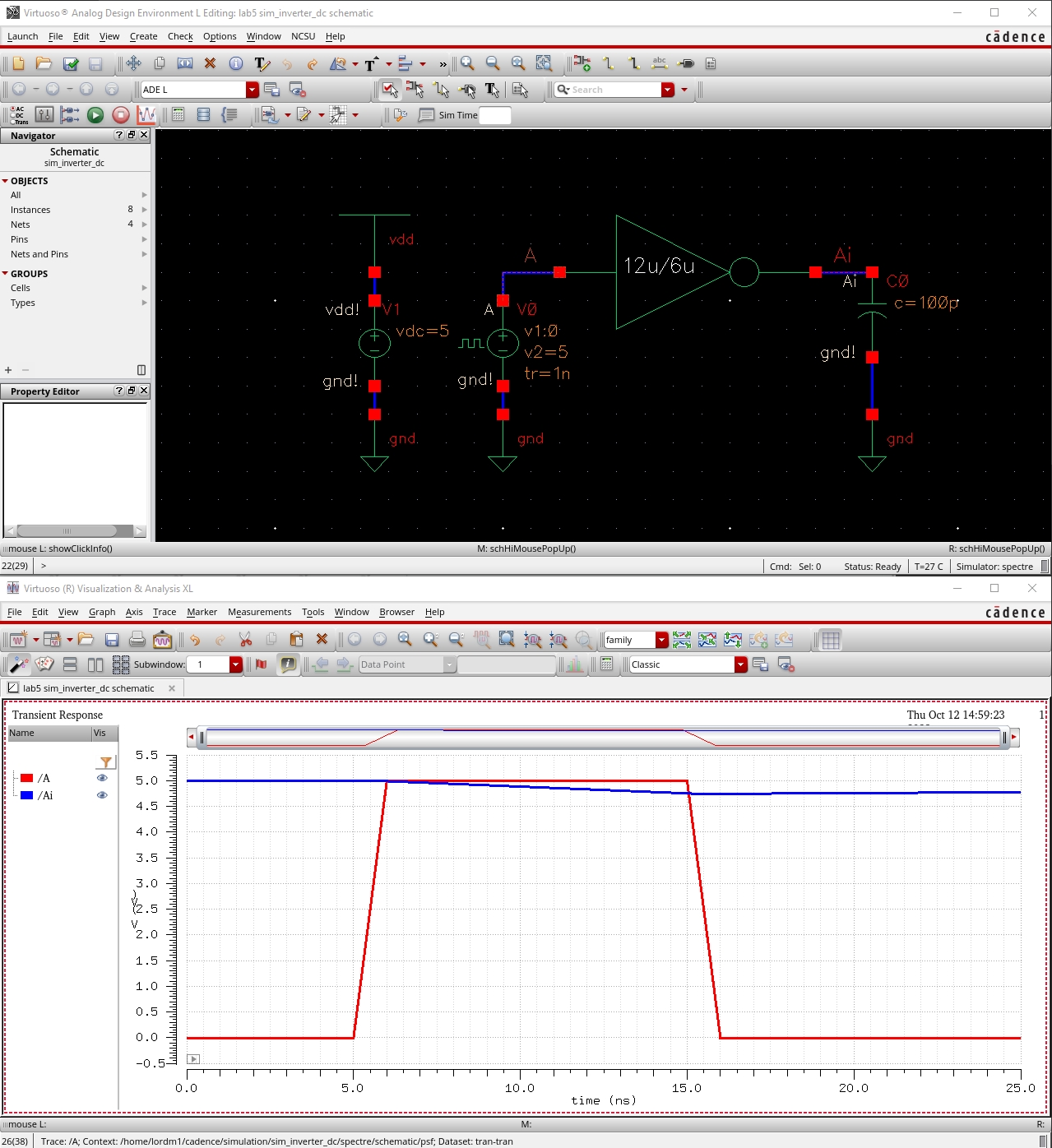
12u/6u Inverter (Width of PMOS / Width of NMOS)
Symbol for my 12u/6u inverter.
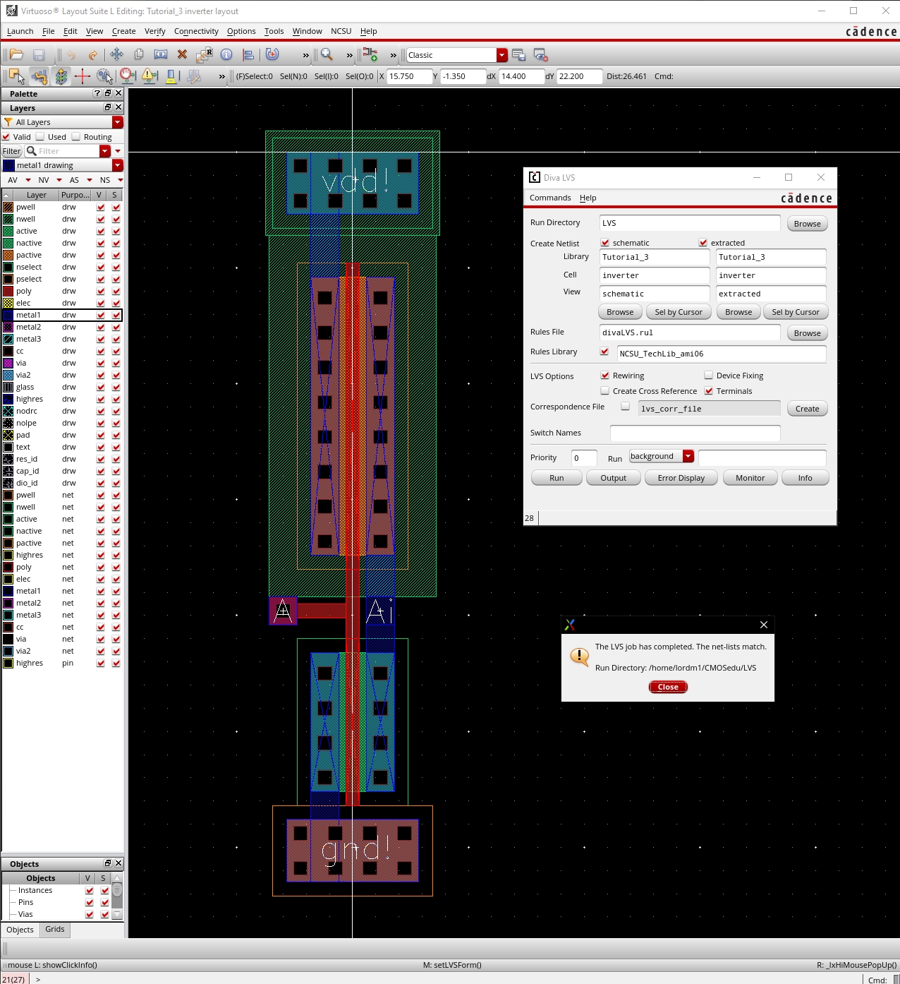
Layout showing good LVS of my 12u/6u inverter.
Simulations using Spectre.

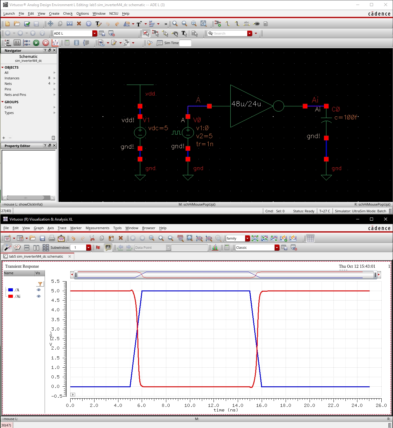
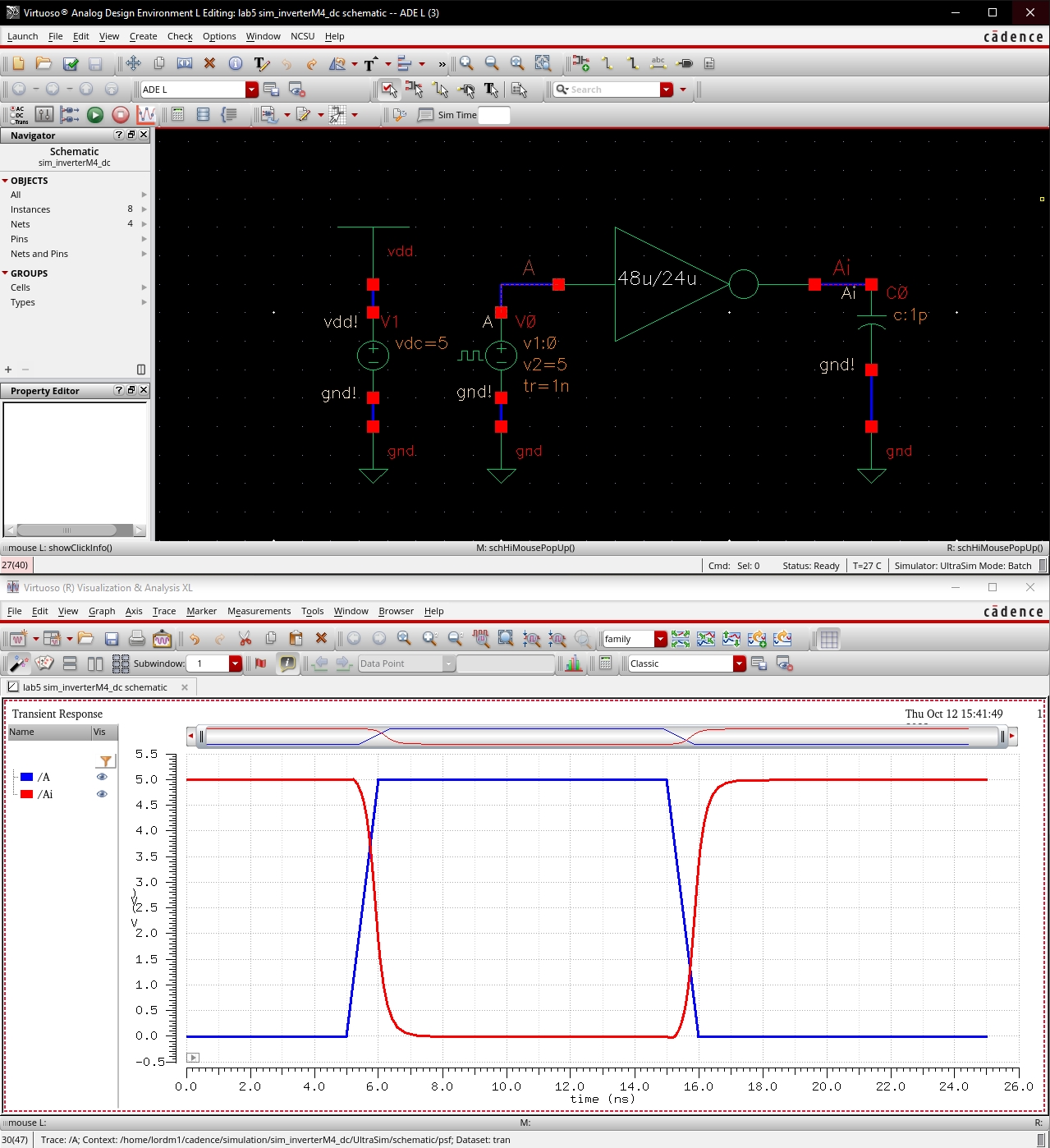
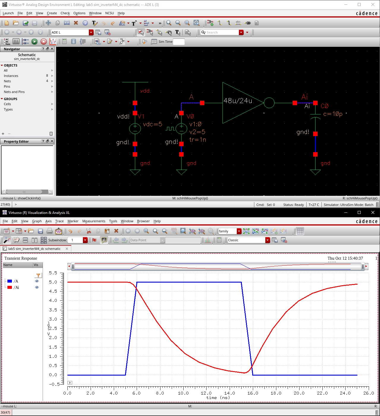
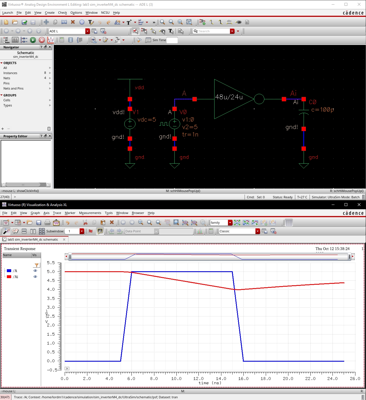
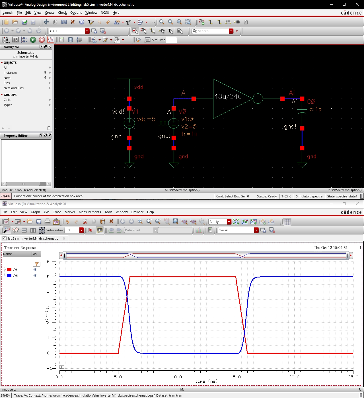
48u/24u Inverter (Width of PMOS / Width of NMOS)
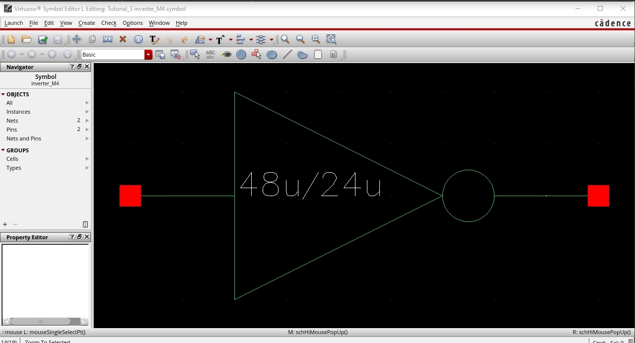
Symbol for my 48u/24u inverter.
Layout showing good LVS of my 48u/24u inverter.
Simulations using Spectre.
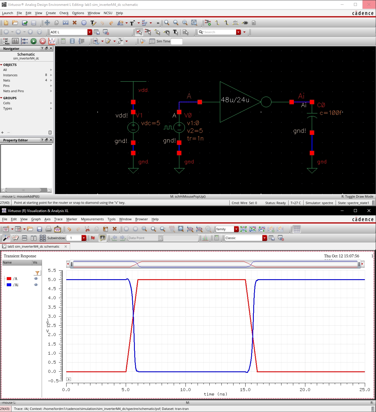
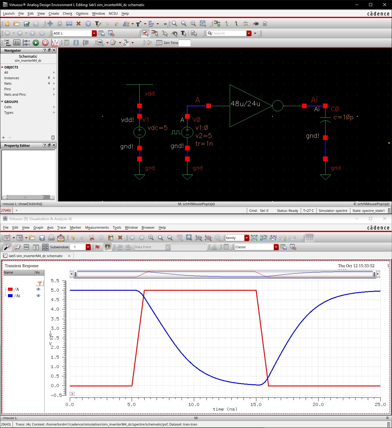
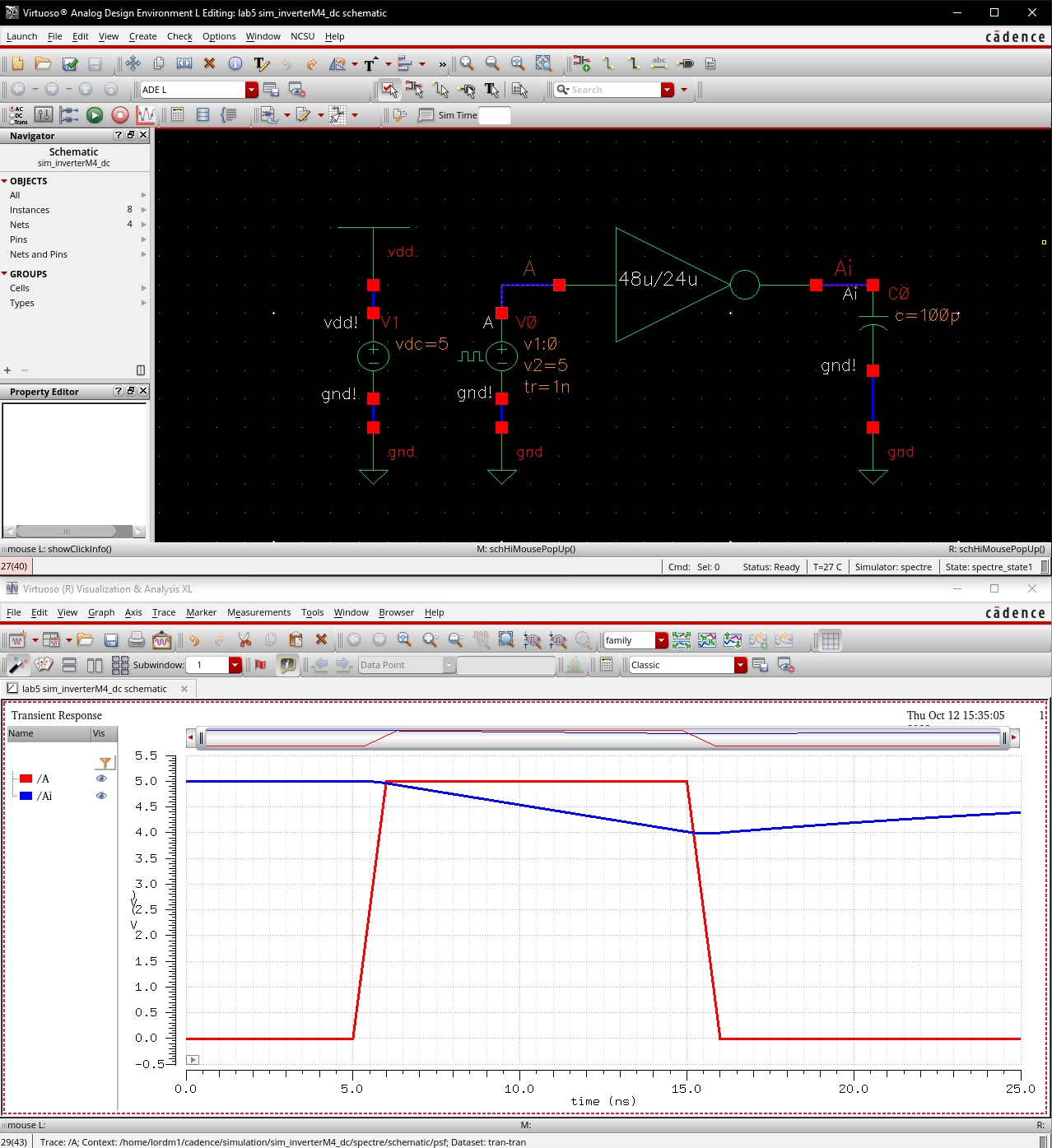
We can observe from the simulations that the four finger inverter performs better because the additional fingers or branches of the MOSFET allow the capacitor to more efficiently charge and discharge.