Lab 4 - ECE 421L
Prelab:
Before beginning
simulations, we needed
to create schematics and symbols for the transistors that we would be
using.
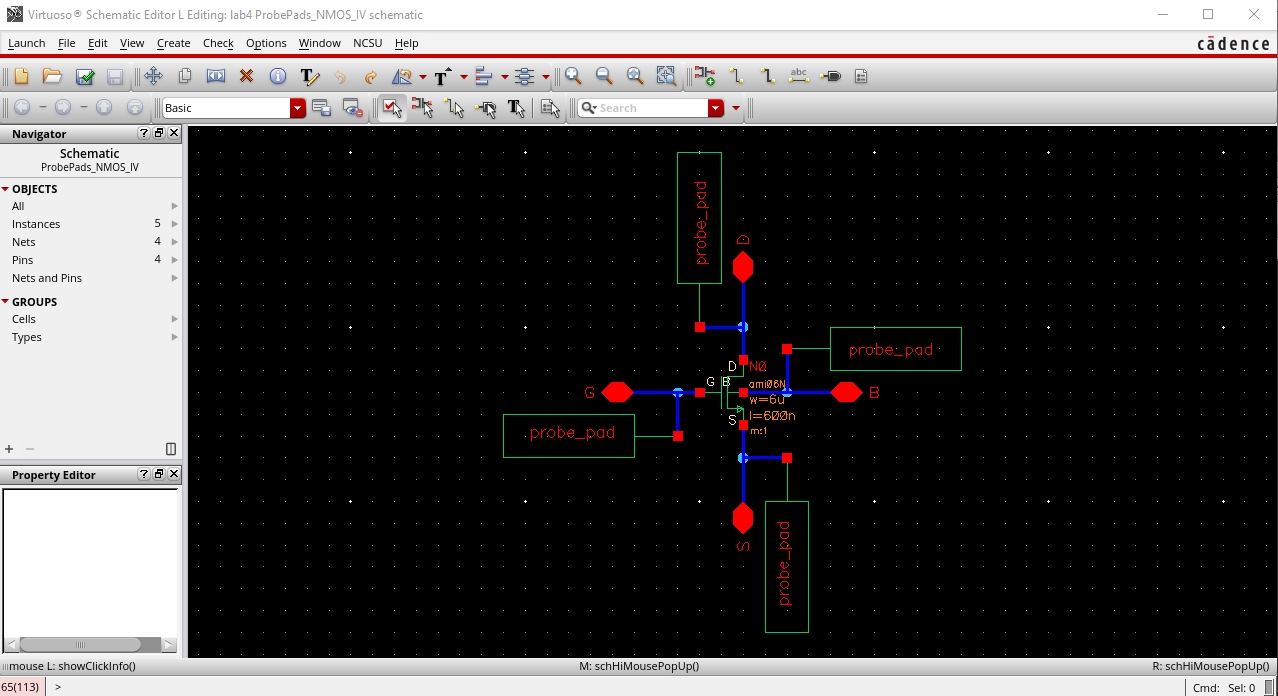
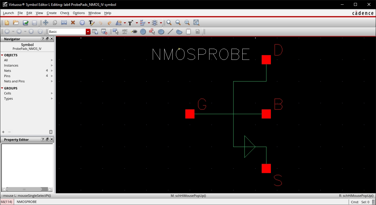
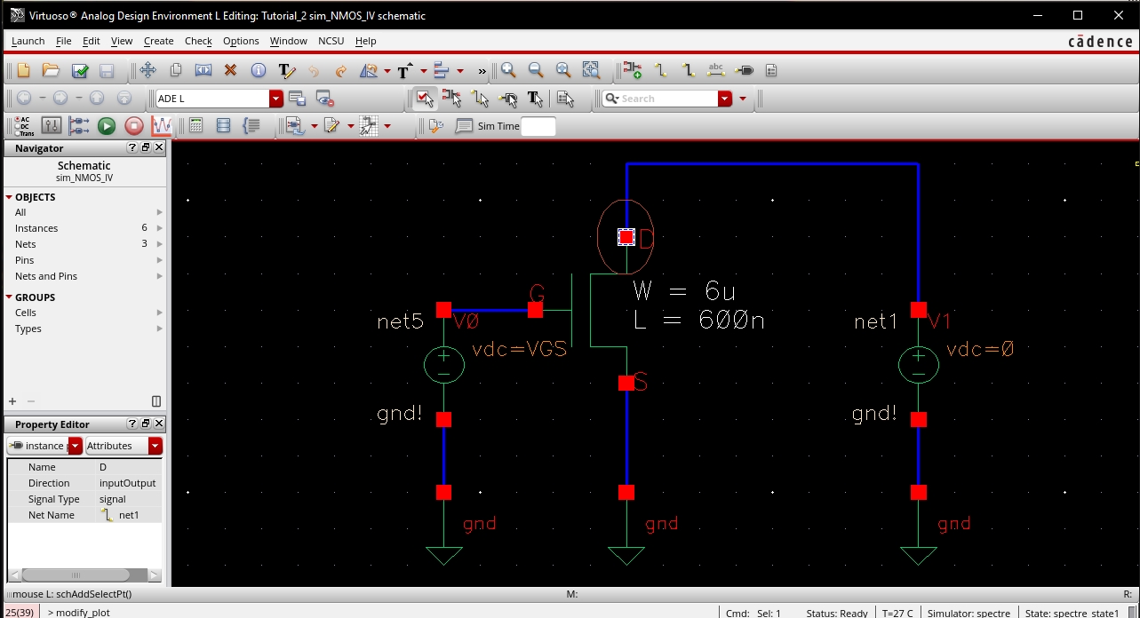
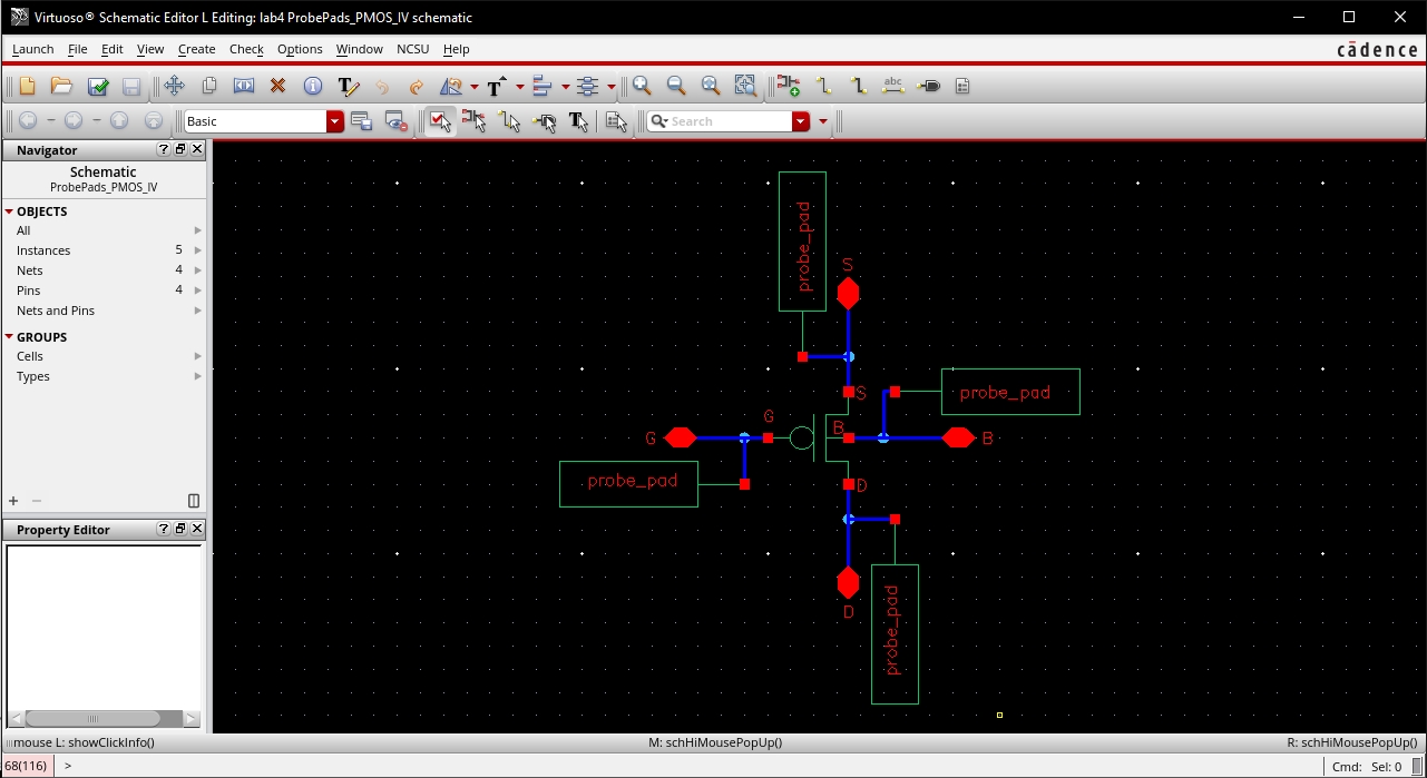
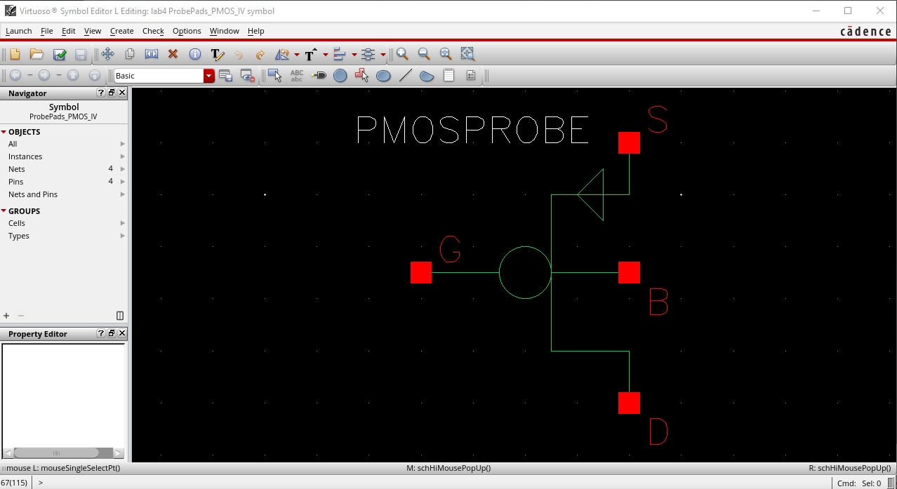
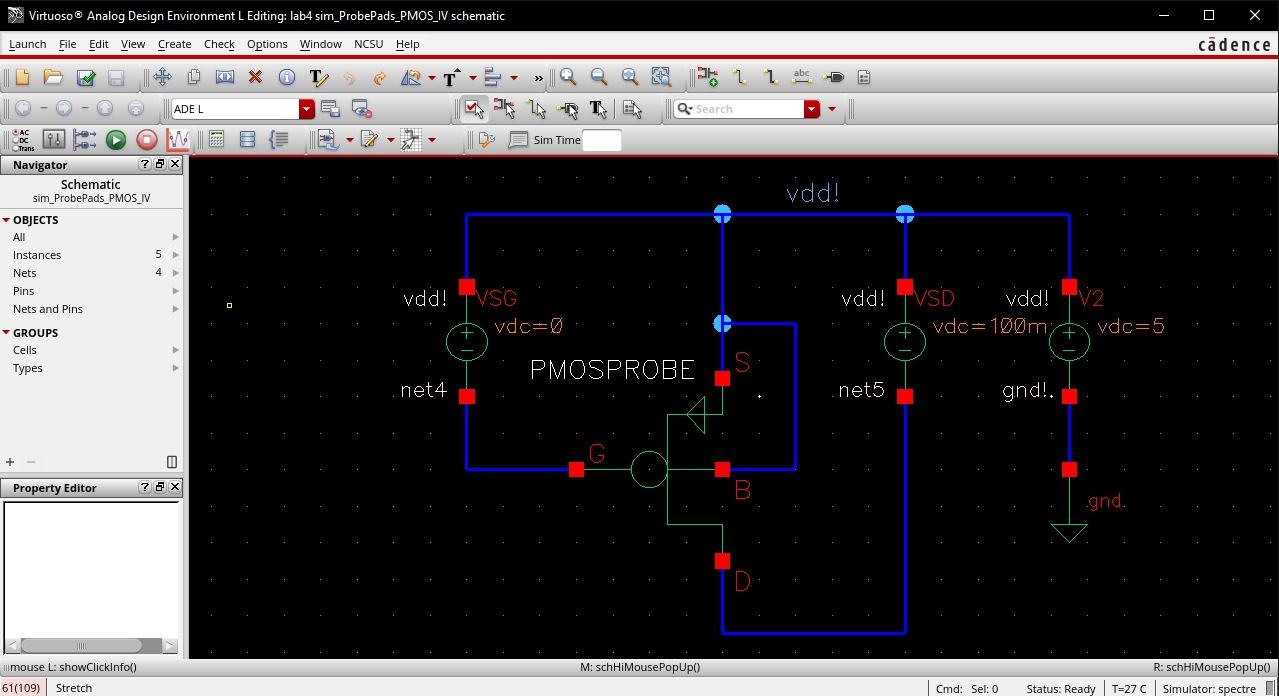
NMOS
Schematic and Symbol
·
In the first
simulation, we let VDS vary
from 0 to 5V in 1mV steps, and we sweep VGS from
0 to 5V in 1V steps.
·
We also set the
length of the NMOS to
600 nm, and the width to 6 microns.
Shown below
are the schematic and the IV curves of this NMOS with the given
parameters.
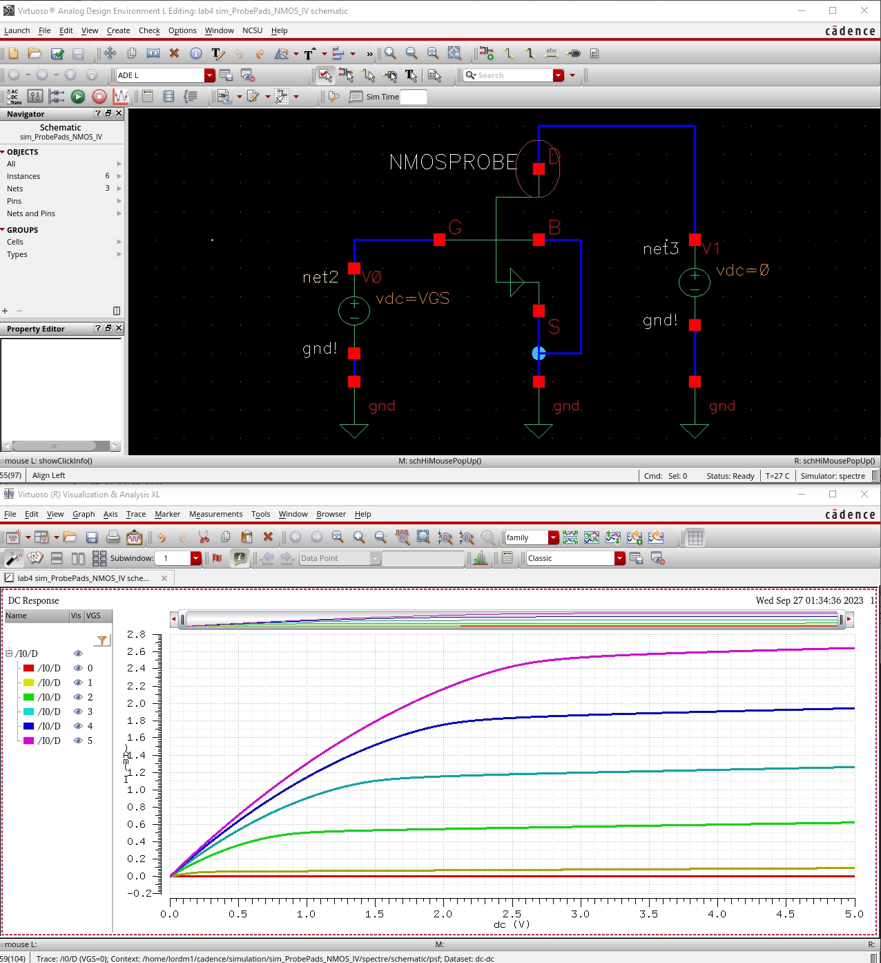
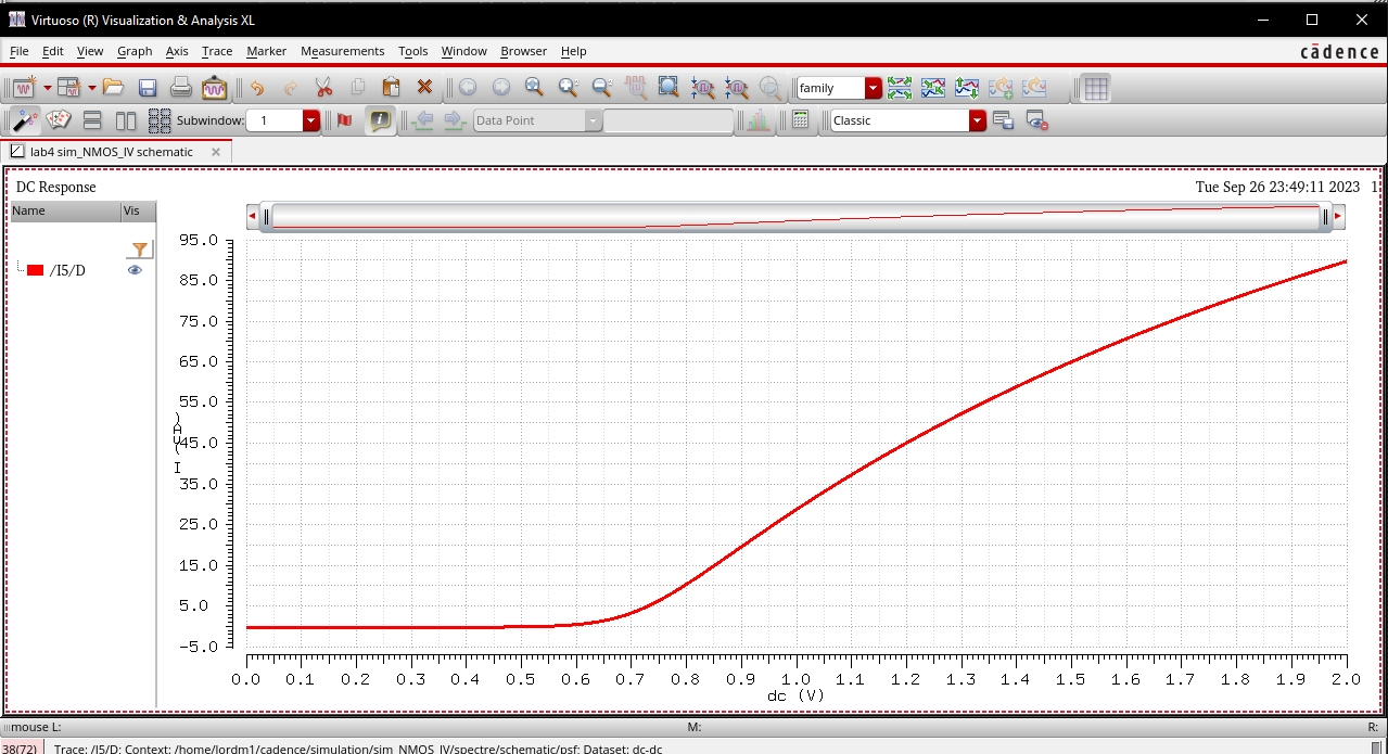
ID
v. VGS of NMOS Device
·
In the second
simulation, we set VDS at
a constant value of 100mV, and we sweep VGS from
0 to 2V in 1mV steps.
·
We keep the same
length and width of our
MOSFET, and instead of simulating ID v. VDS
as we did previously, we simulate
ID v. VGS.
The schematic and IV curves are shown below.
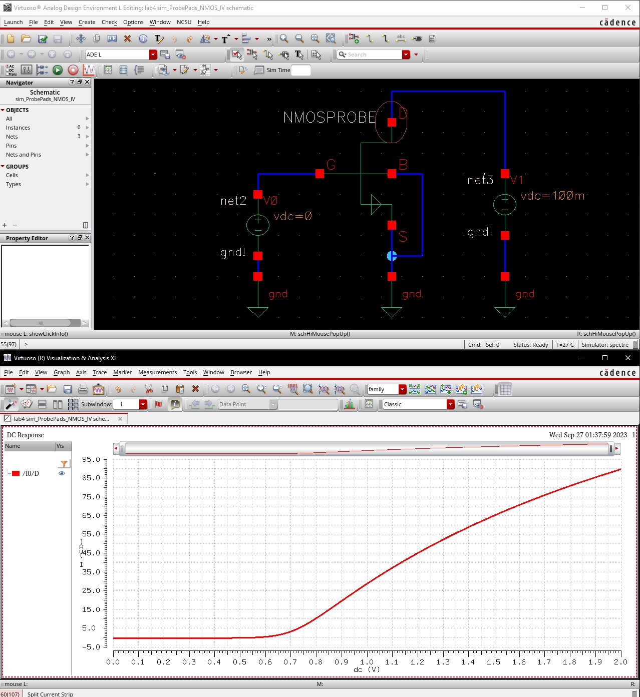
ID
v. VSG of PMOS Device
·
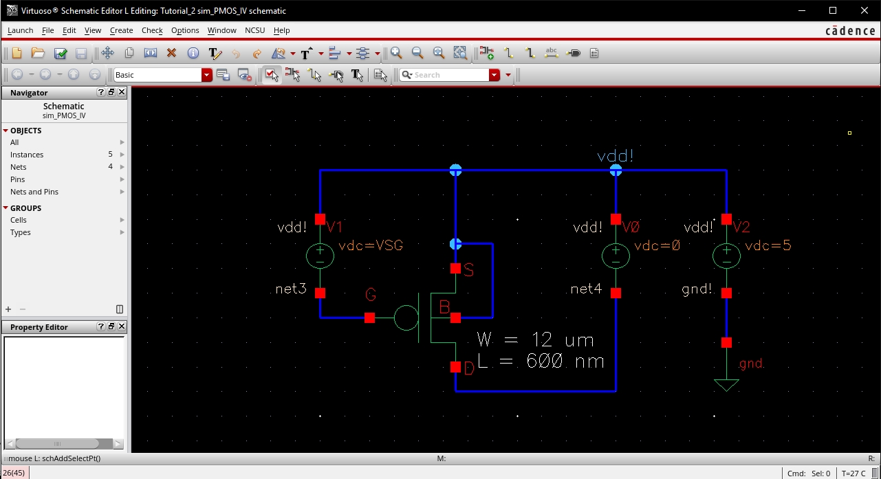
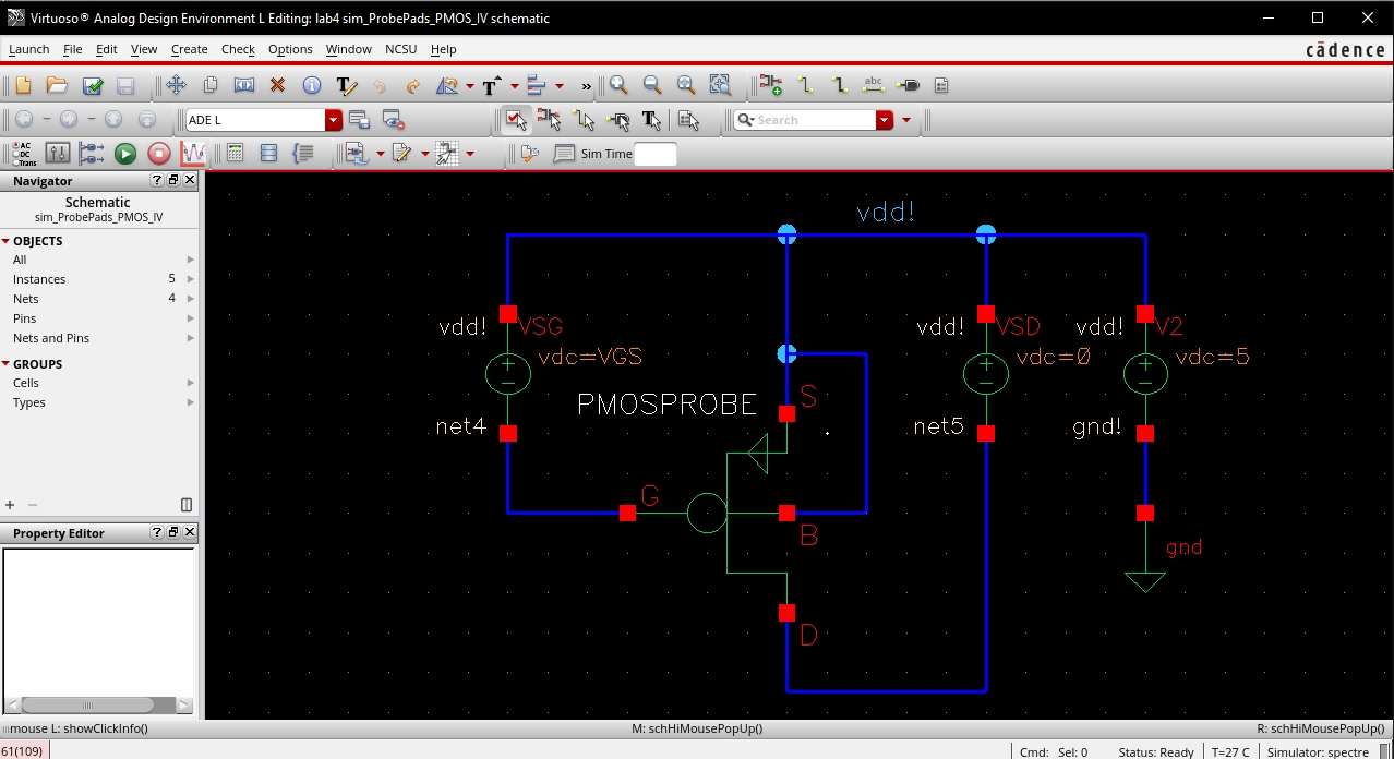
The third
simulation calls for a sweep
of VSG from 0 to 5V in 1V steps, and VSD should vary from 0 to 5V in 1
mV
steps.
·
The width of the
PMOS is changed to 12
microns, while the length is kept at 600 nm.
·
Note that the base
of the PMOS is tied
to VDD in this schematic. In the NMOS schematics, the base was tied to
ground.
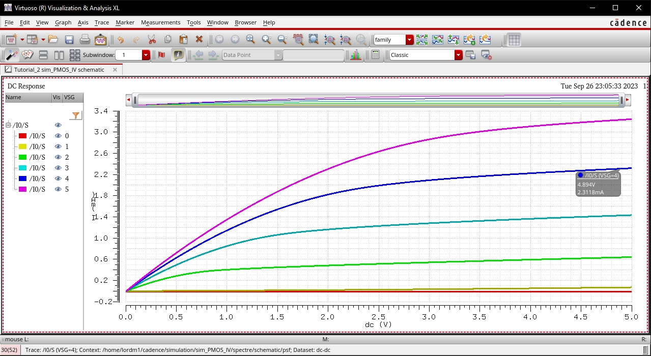
ID
v. VSG of PMOS Device
Using the
same width and length of the previous MOSFET, we observe the results
below.
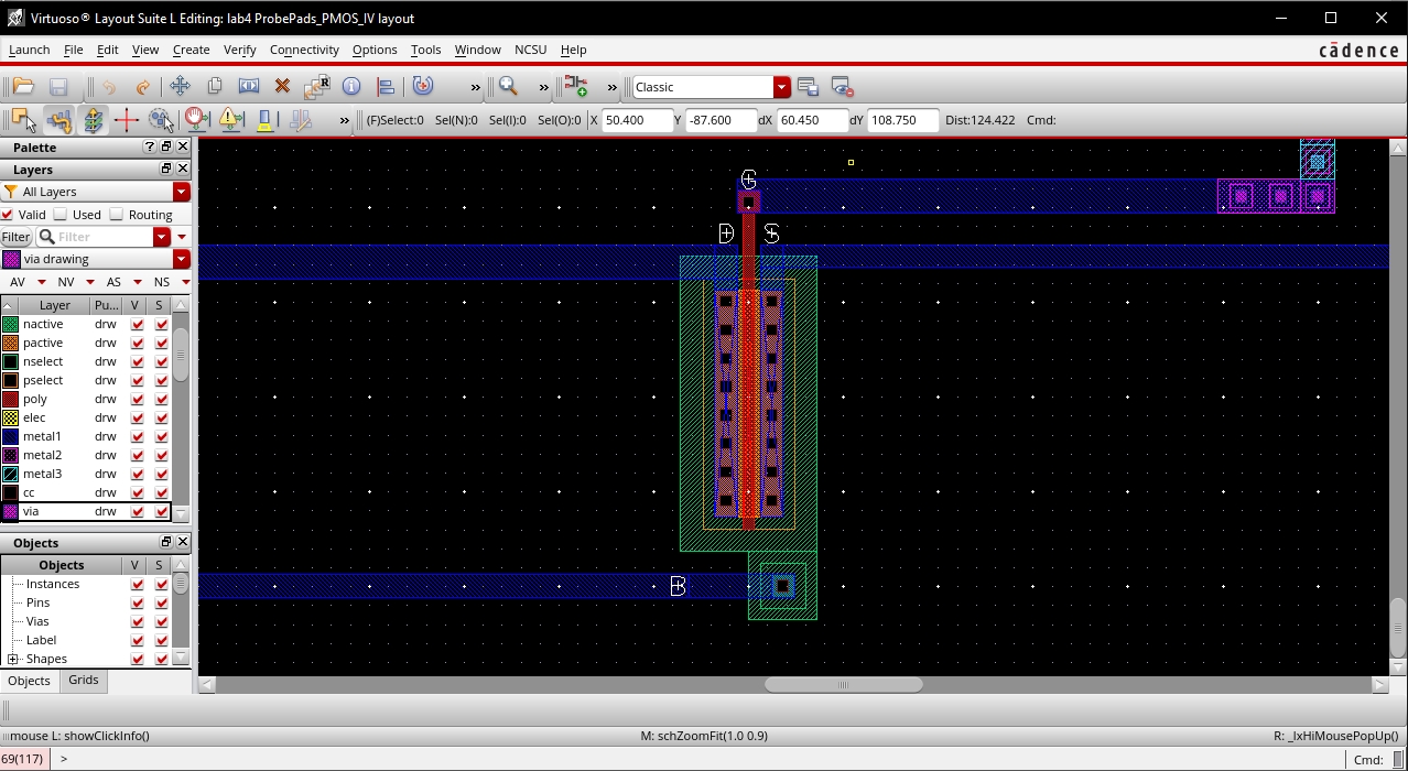
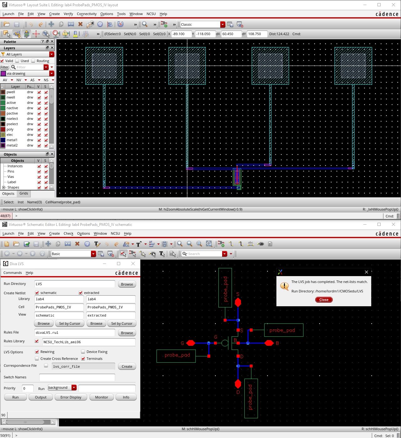
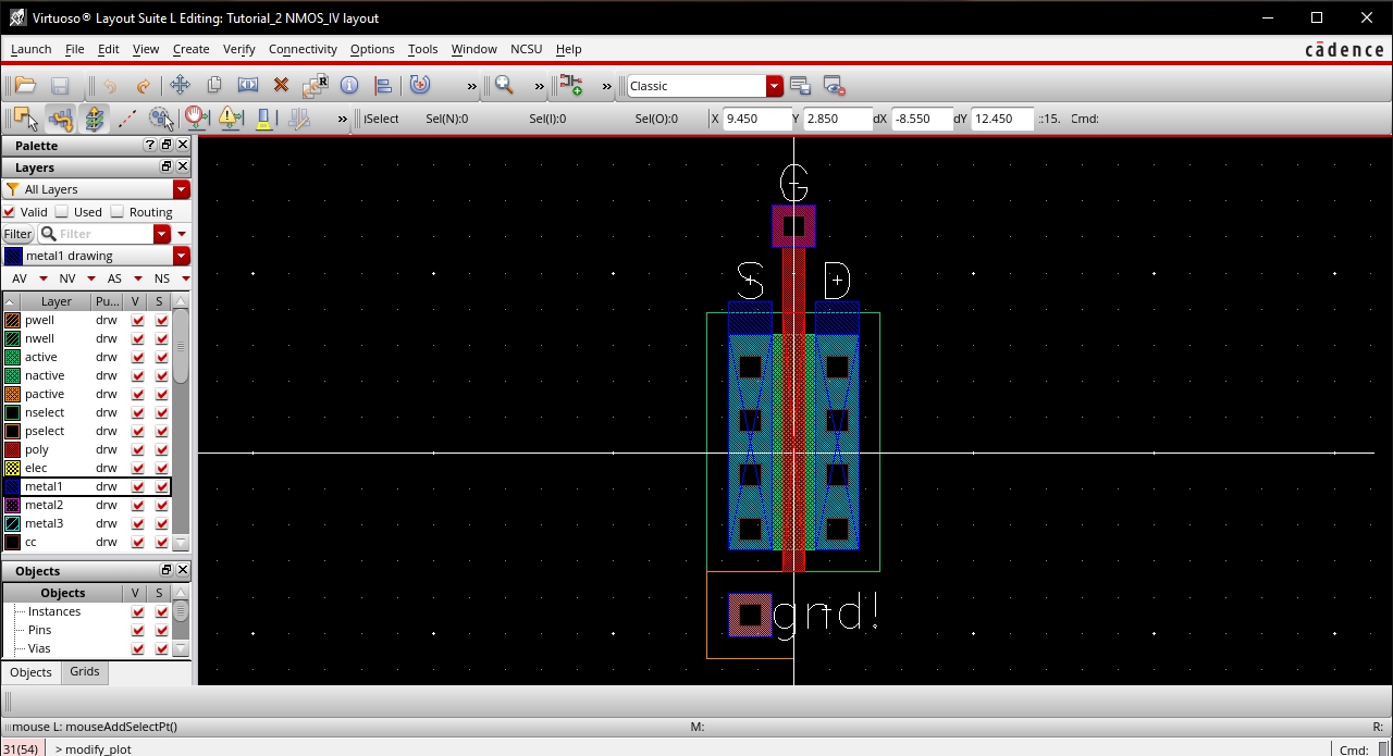
Layout
of 6.0u/0.6u NMOS Device
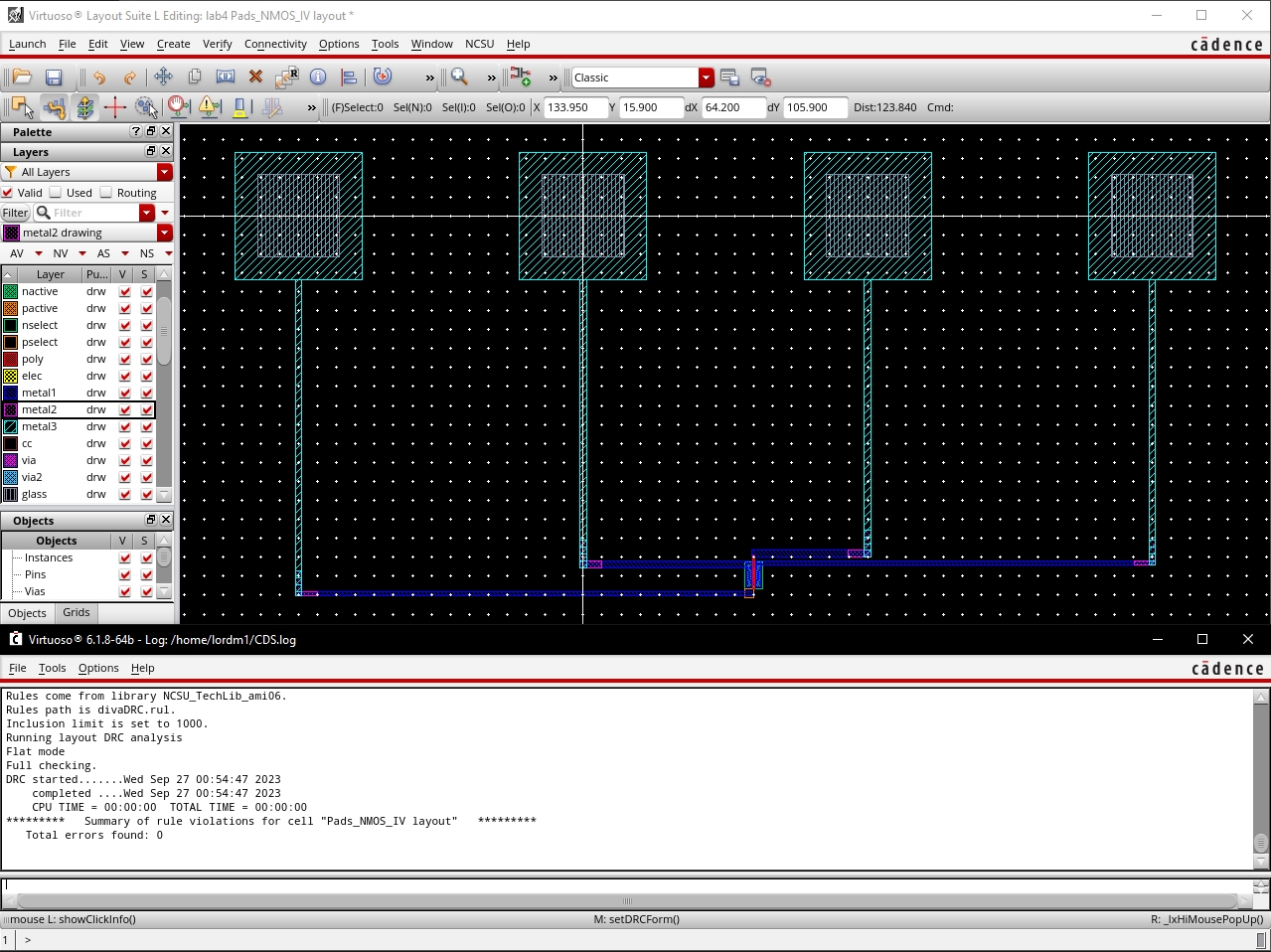
Full Layout of NMOS
Including Probe
Pads with DRC.
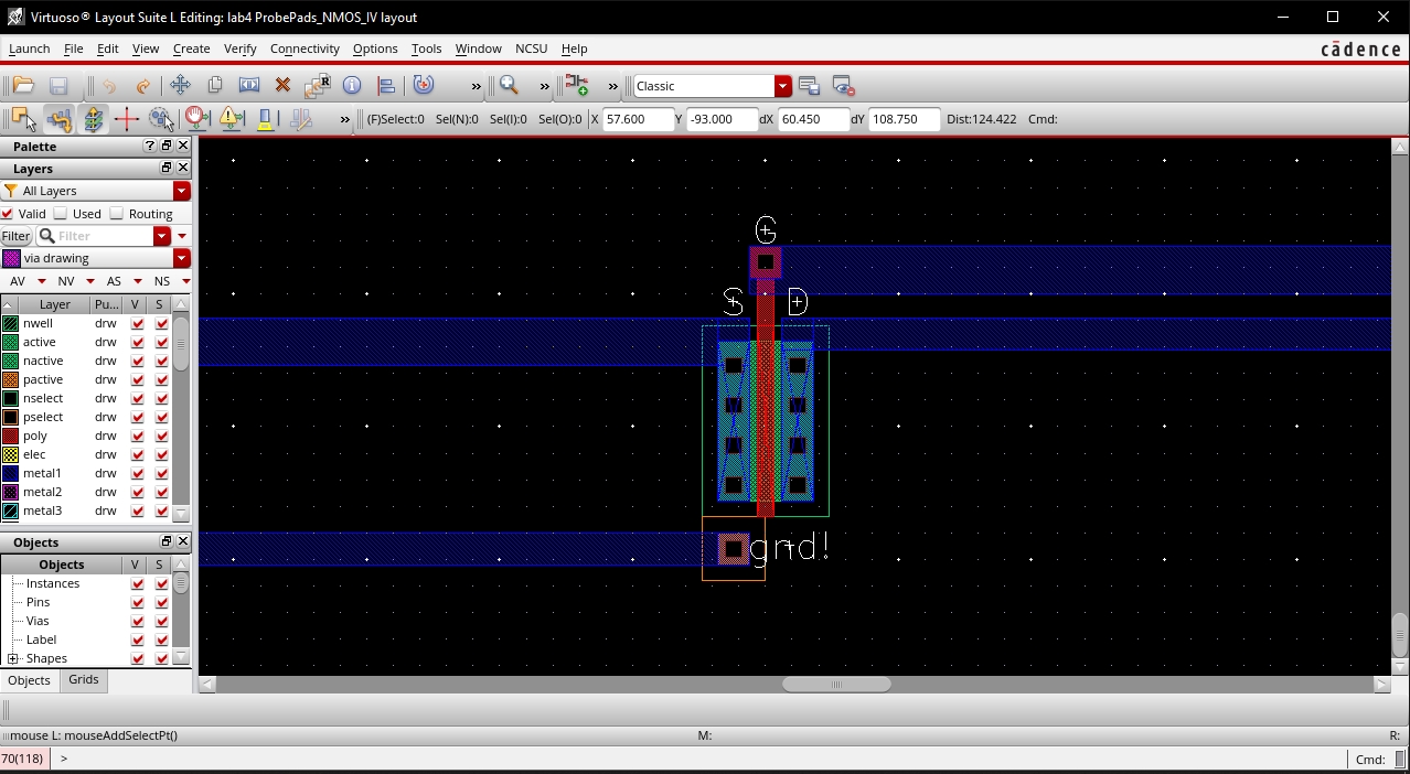
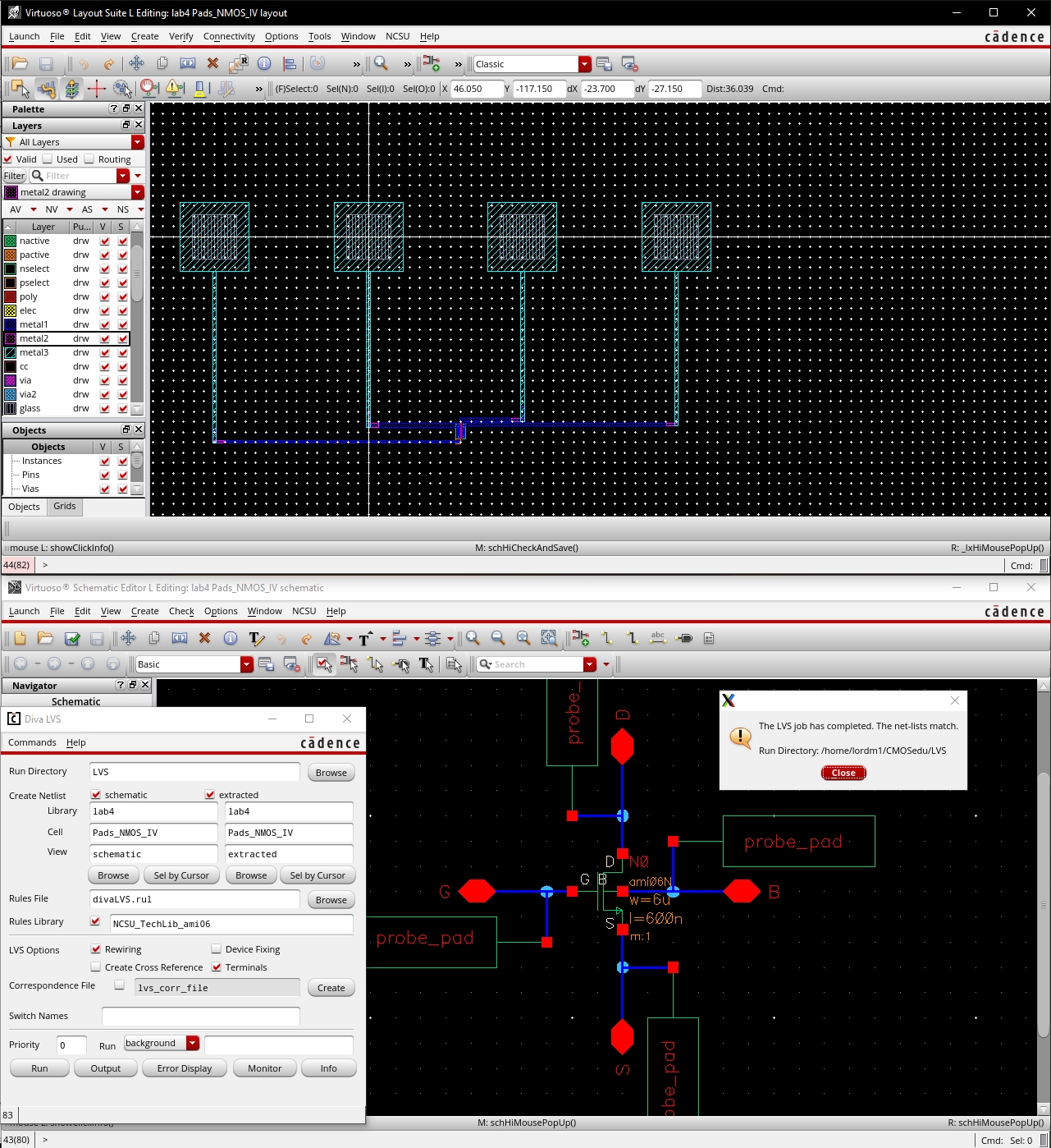
Zoomed-In View of
Layout of NMOS
Device & LVS Verification
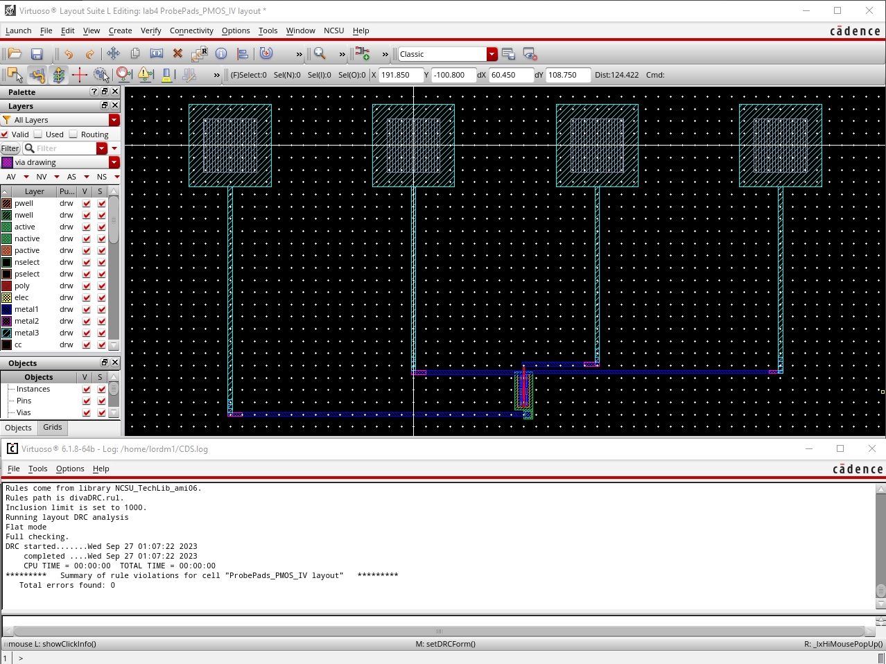
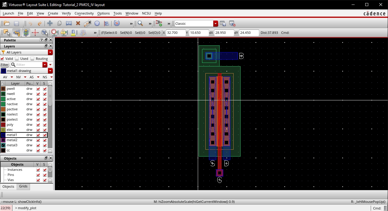
Zoomed-In View of Layout of PMOS
Device & LVS Verification