Lab 3 - ECE 421L
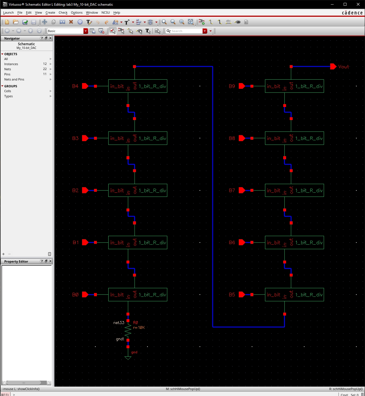
The purpose of Lab 3 is to layout the 10-bit DAC that was designed in Lab 2.
Prelab:
I use a RAID 1 config on my main computer with the important files being backed up to my cloud, along with a second computer in my livingroom that downloads any changes to my files in the cloud, so all in all I have 2 physical locations using RAID 1 along with my cloud backup.
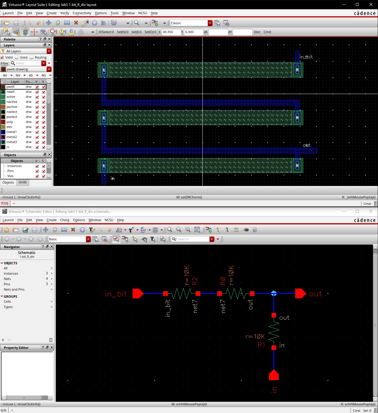
Below you can see the layout used for tutorial 1 and the DRC.
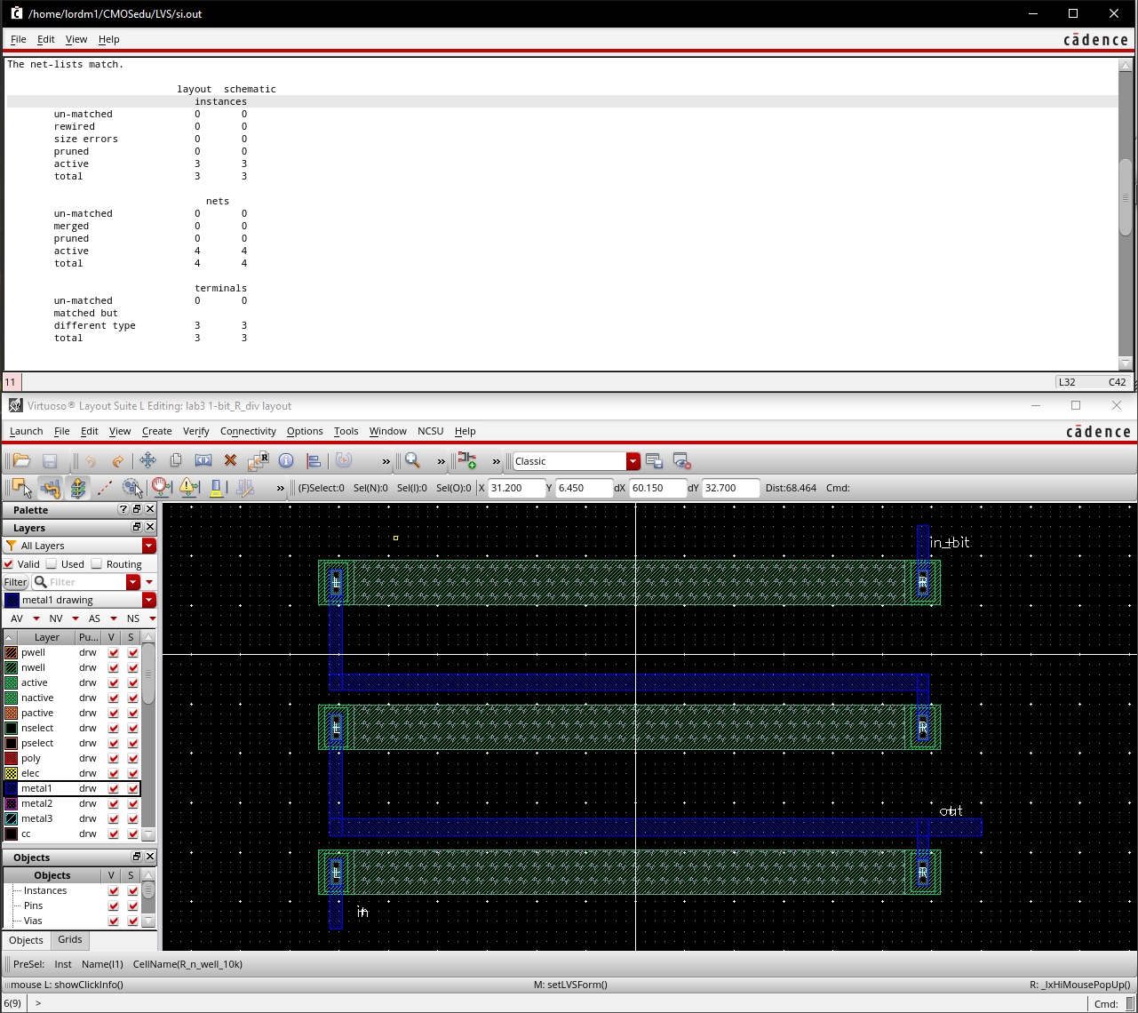
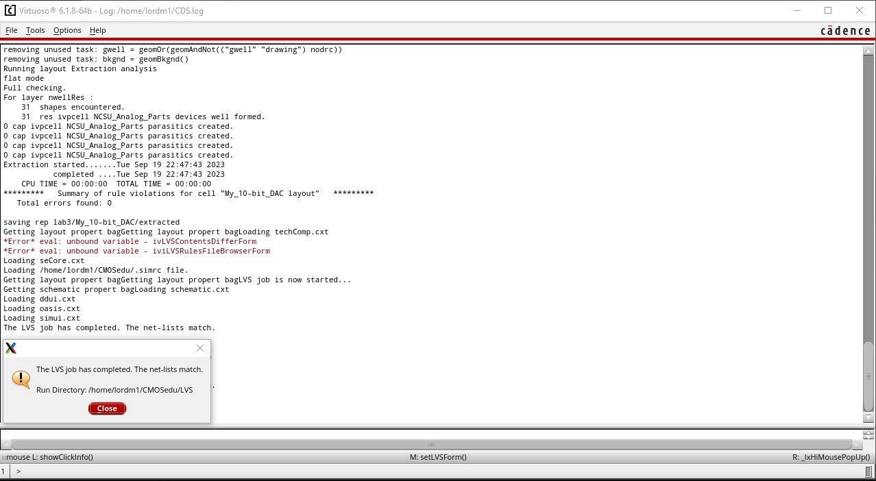
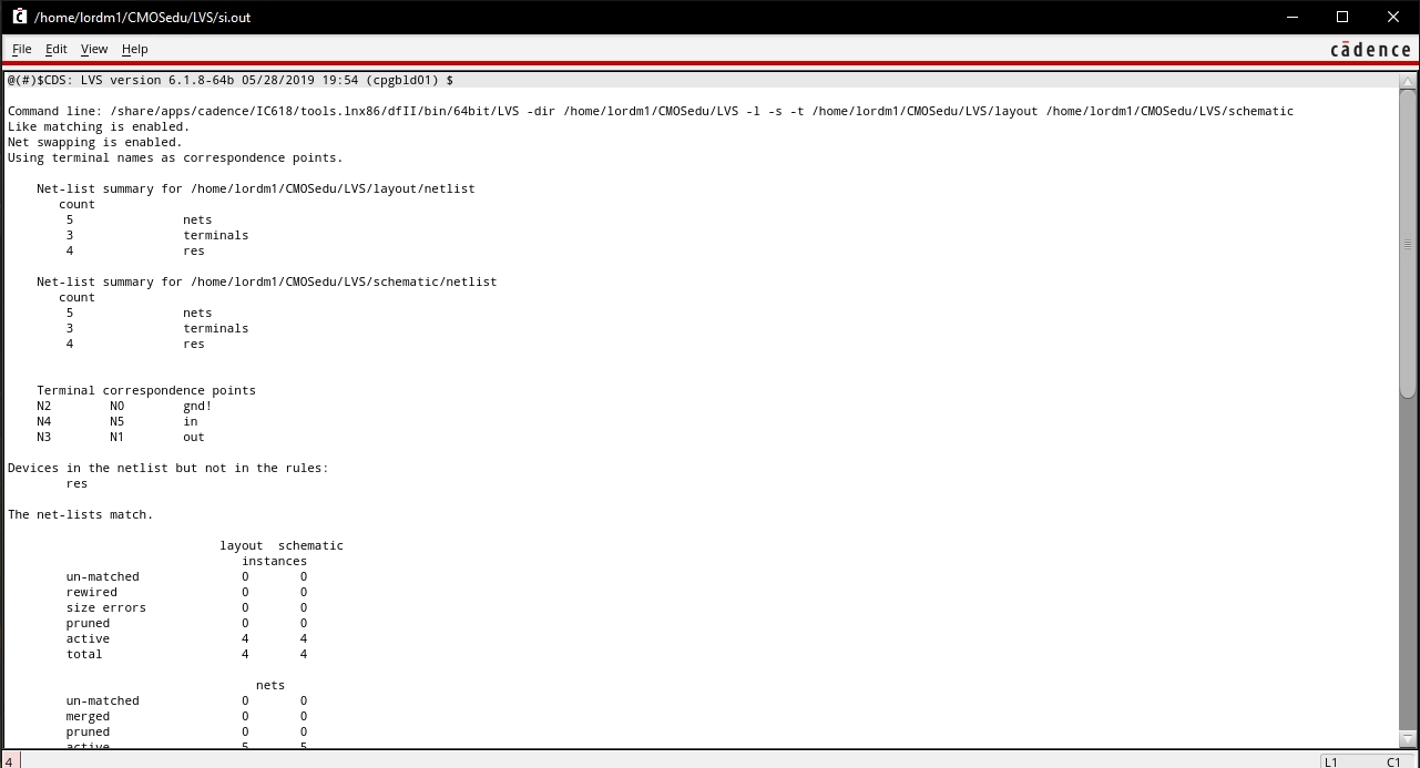
As seen below I successfully completed tutorial 1 with the netlists matching after running the LVS on my R_div.
I started this lab by copying in some of my files from lab 2 that would be used for this lab.
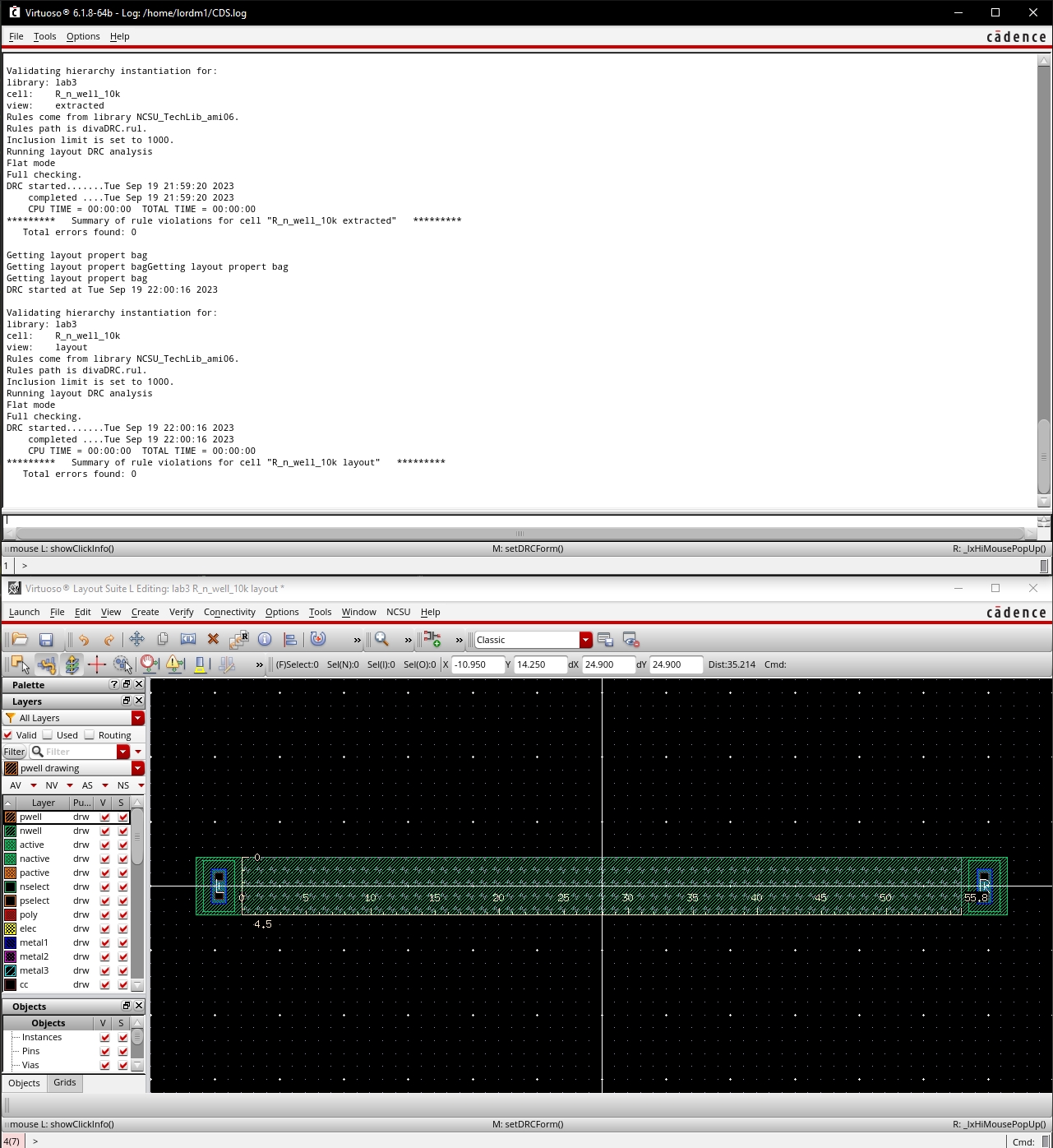
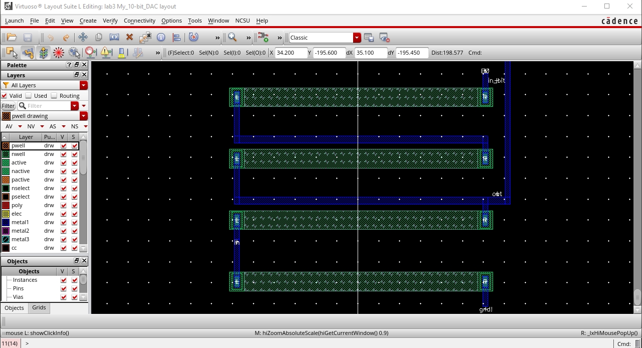
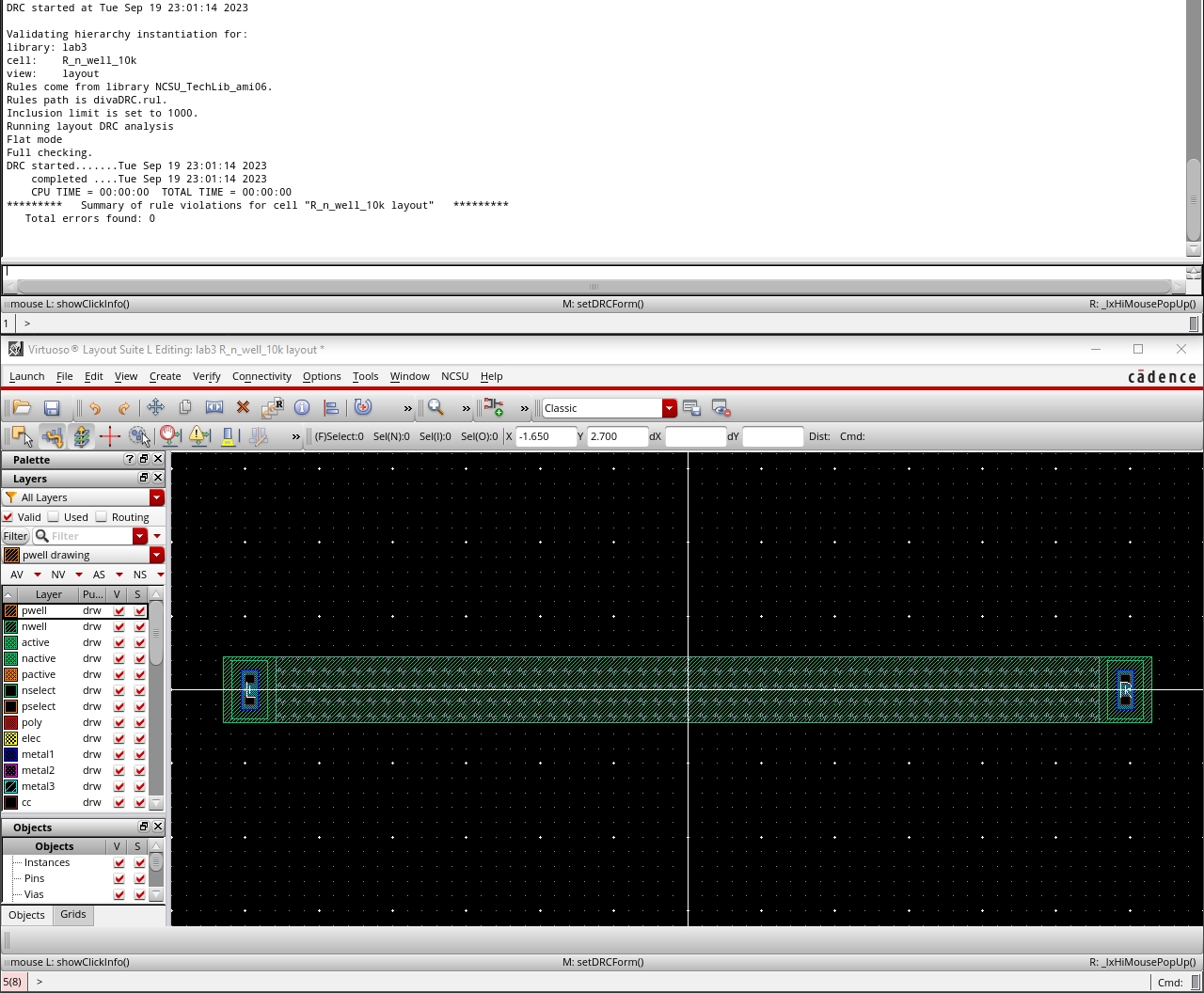
The coponent we would need to create was a 10k resistor using the equations below to find the dimensions needed.
R = Rd * (L/W)
R = 10k Ω
Rd = 800
W = 4.5 microns
10k = 800 * (L/4.5 microns)
L = 56.25 microns (due to the pins skewing the resistance the length I ended up needing was 55.8)
To accomplish the needed resistance I used 55.8 microns by 4.5 microns.
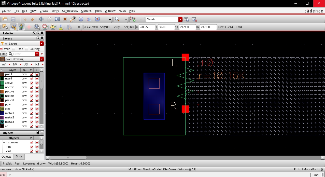
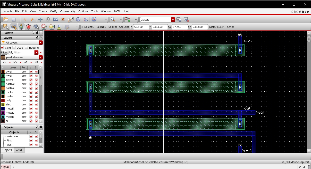
Below is a picture of the resistor with a ruler showing measurements used as well as a DRC of the layout.