Lab 2 - ECE 421L
The goal of Lab 2 is to utilize n-well resistors to create a 10-bit Digital to Analog Converter.
Prelab:
Our first step is to back-up our work, I have backups from the cloud as well as in two different physical locations.I made sure to add DEFINE lab2 $HOME/CMOSedu/lab2 into cds.lib, so I can access the lab2 files within Cadence.
After launching cadance we can see that the files were in my library manager and I was able to open sim_Ideal_ADC_DAC without any problems.
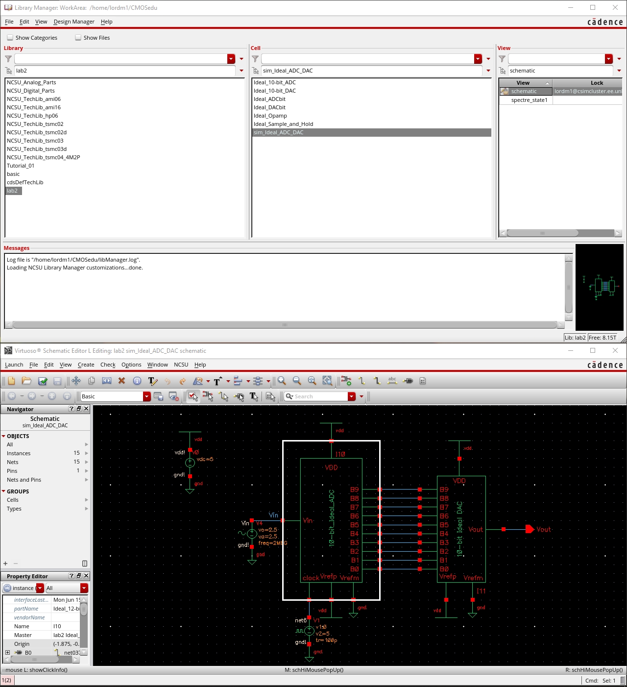
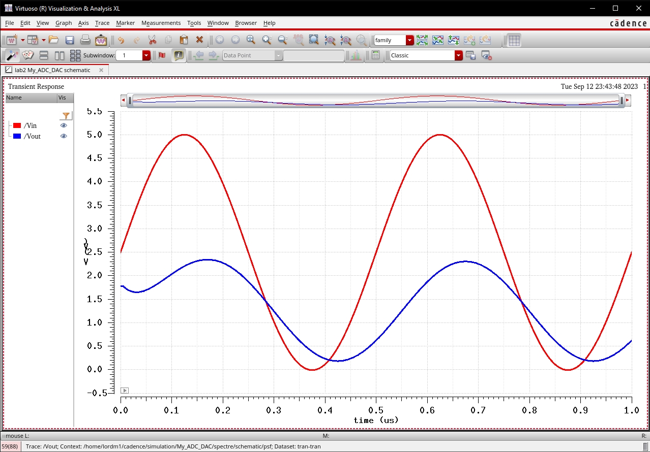
I launched the analog design environment to get a better understanding of what our circuit is doing. Once inside the ADE, the simulation went as expected without any kind of smoothing capacator on our output.
Determining the Least Significant Bit
The LSB is the minimum voltage needed for the output to be altered by the ADC for the DAC to properly read its value.
Using the below equation we can calculate the LSB.
LSB = Vdd/(2^n)
Vdd is the source input that is running into into the ADC.
n is the number of bits that are being outputted by the ADC.
Since there are 10 bits being output by the ADC, 210 will give us the number of possible binary values.
By dividing Vdd by the total amount of possible binary values, we can calculate the LSB.
Vdd = 5V
n = 10 bits
LSB = Vdd/(2n)
LSB = 5/(210)
LSB = 4.88281mV
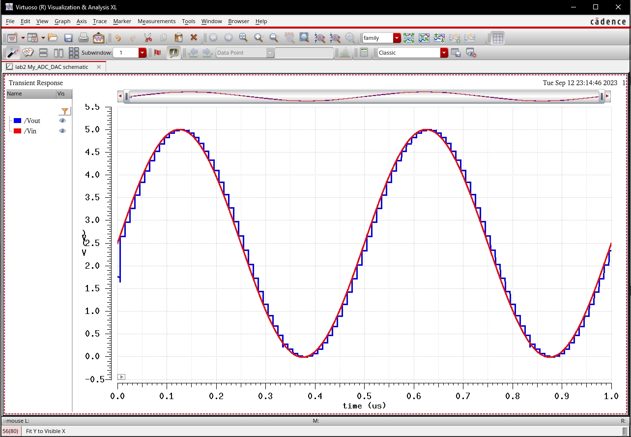
Based on the above calculations, the LSB is 4.88281mV. This means that incrementing the input of the ADC by 4.88281mV will cause the LSB of the ADC bus output to go high.
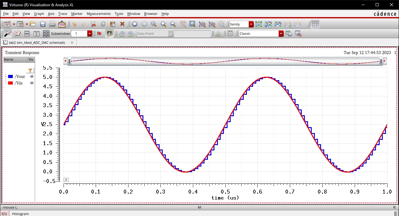
Included below is a simulation of the circuit showing the value 4.88281mV per step just as expected.
We
can see that it doesnt require Vin to actually
reach 4.88281mV as the jump occurs roughly at half of that value
2.4414mV.
Lab Report:
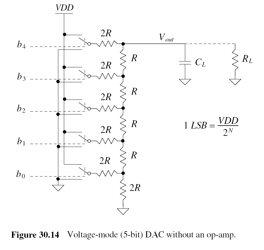
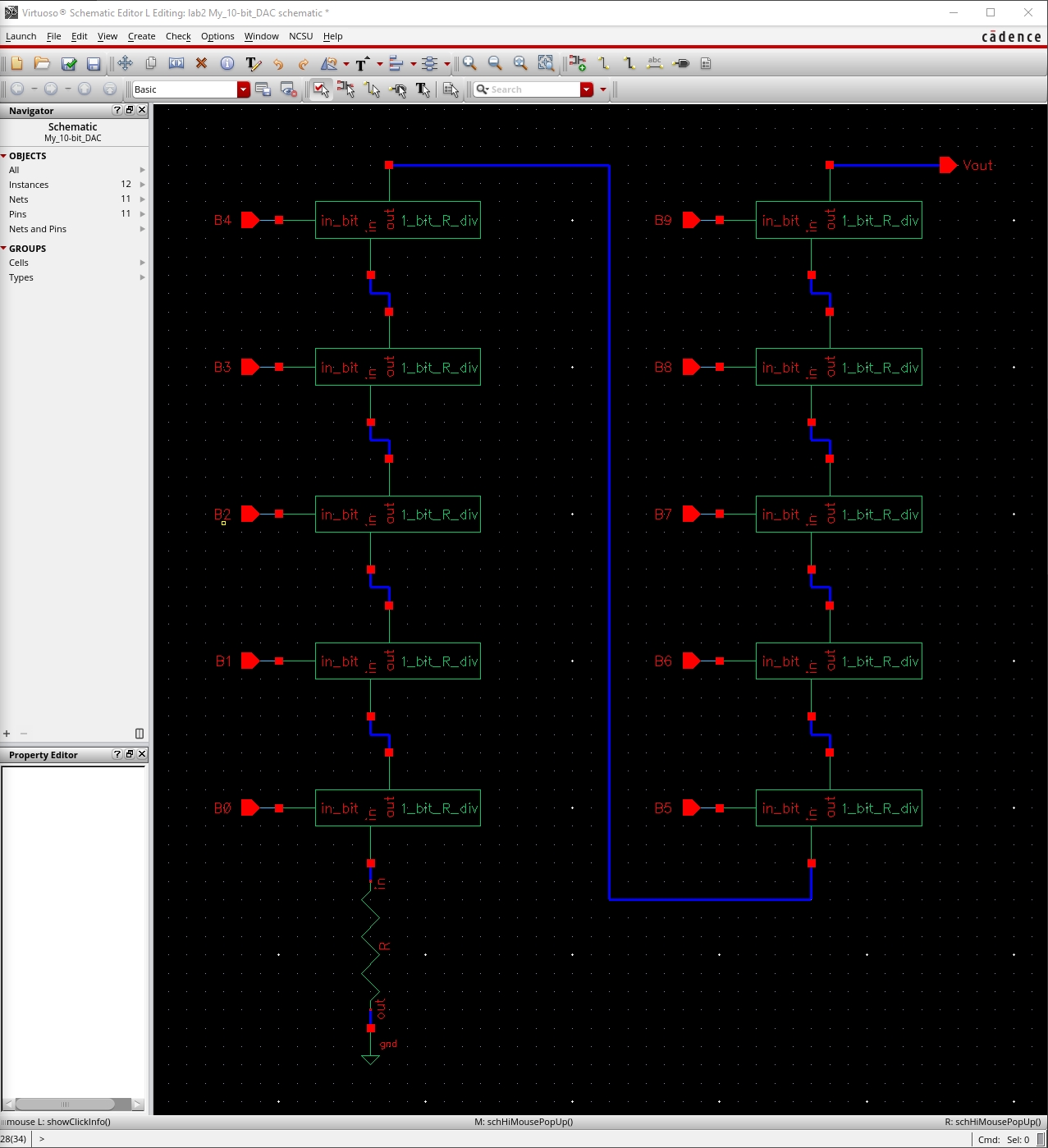
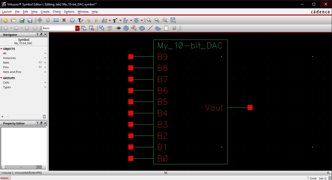
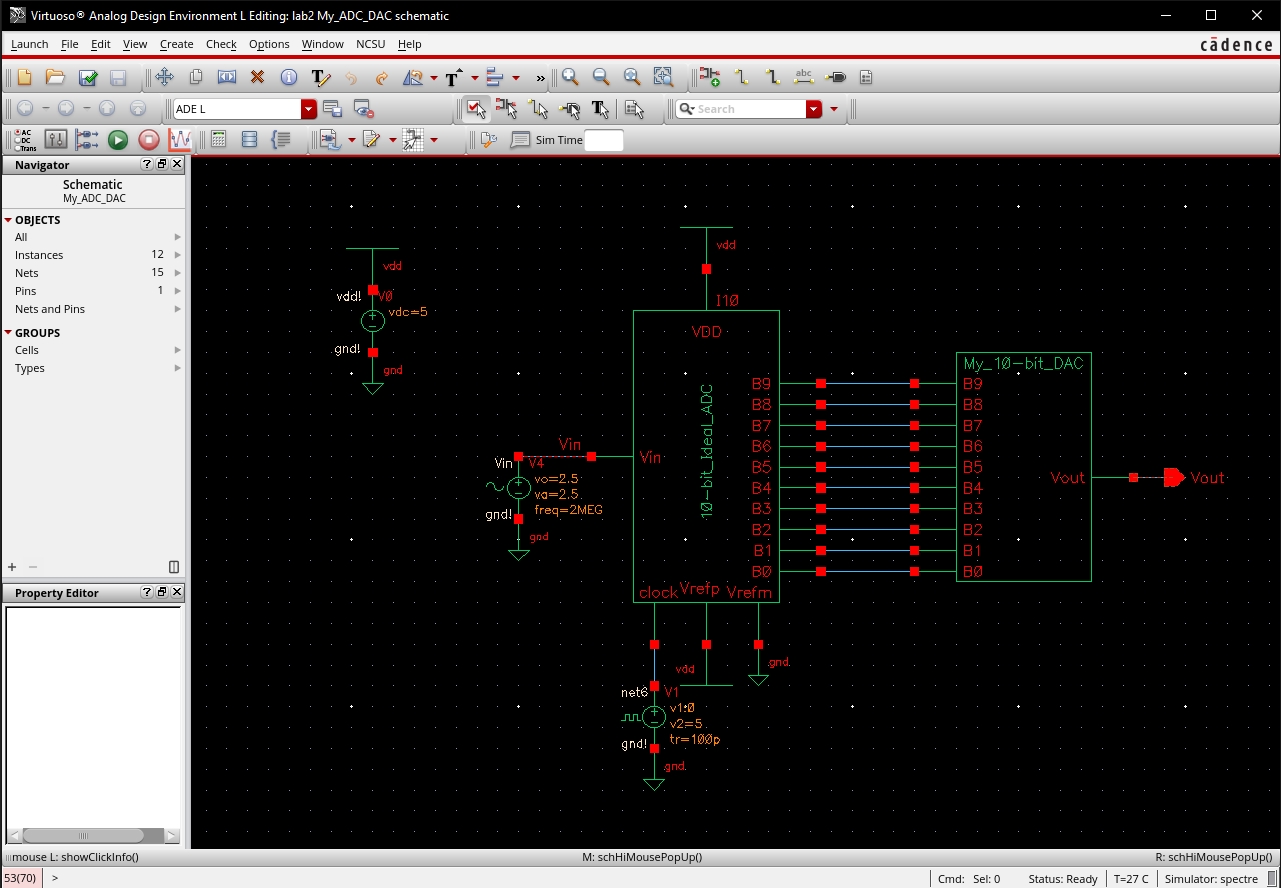
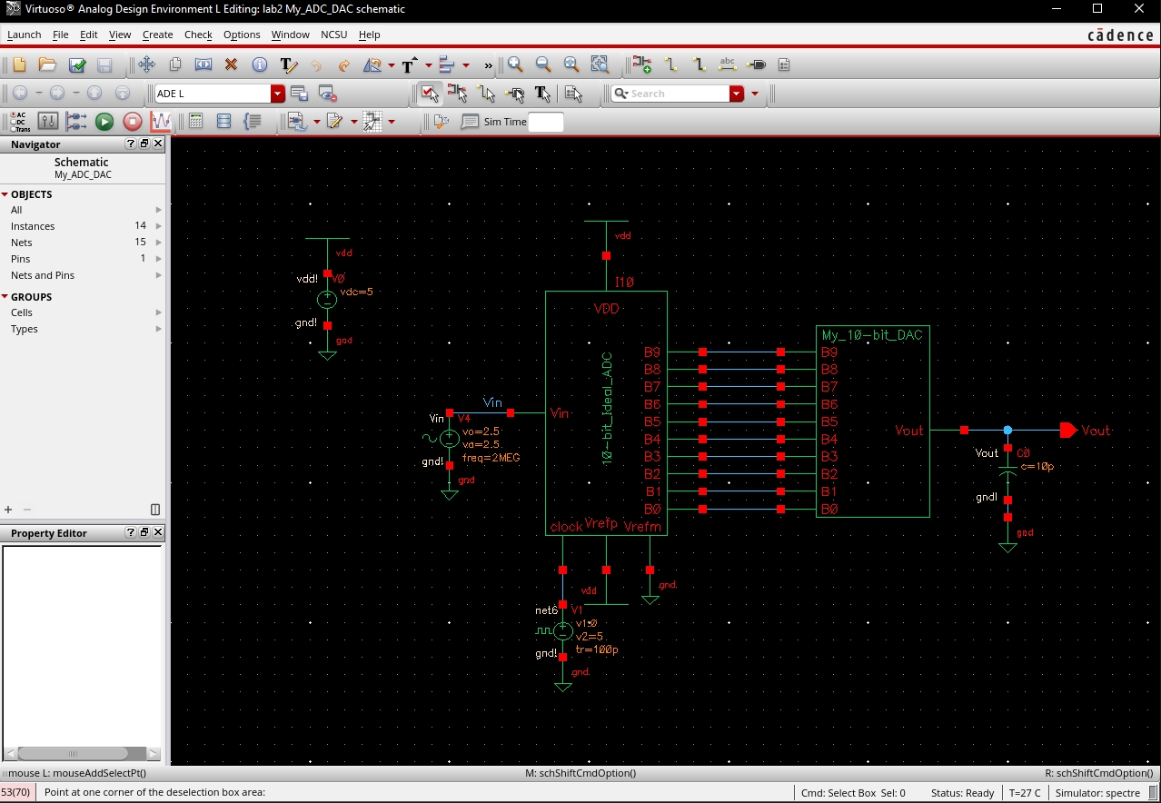
For this lab were going to be using the below figure as a guide for creating our own 10-bit DAC.
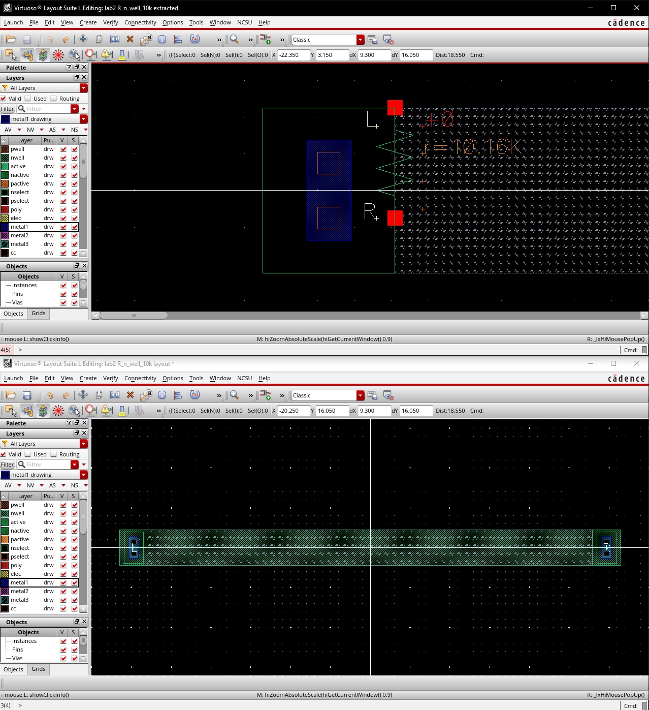
The first step is to create the voltage divider for a single bit, starting off with our layout for a 10K resistor.
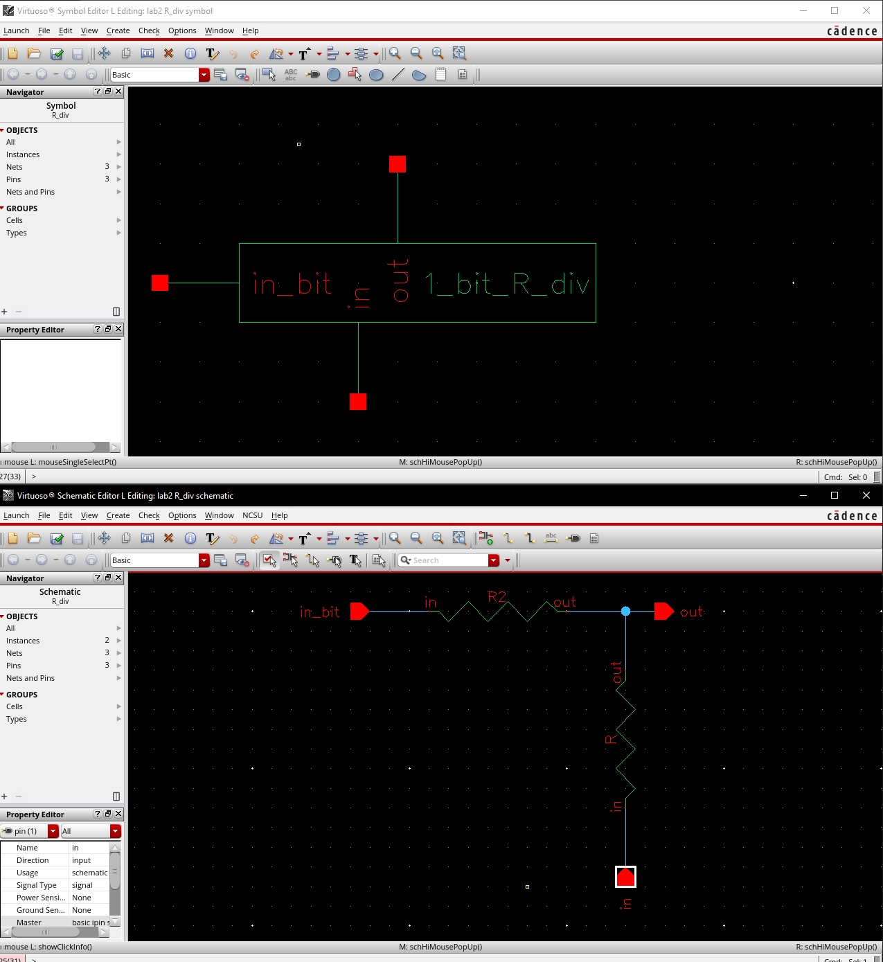
After this I created the schematic for the voltage divider we'd be using for our single bit input as well as a symbol to simplify its use later on.
Determining Output Resistance of DAC
Below are the steps I took in order to find the output resistance of the DAC.
First, I saw that 20k and 20k were in parallel which meant that the resulting resistance was 10k.
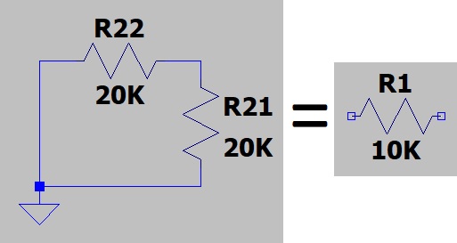
After noticing that the resistor was 10k, I realized that the 10k resistor above was in series meaning we get a 20k resistor going to ground again.
This means that we can work our way up all the way to B9 1-bit divider and figure out the resistance of the DAC is 10K ohms.
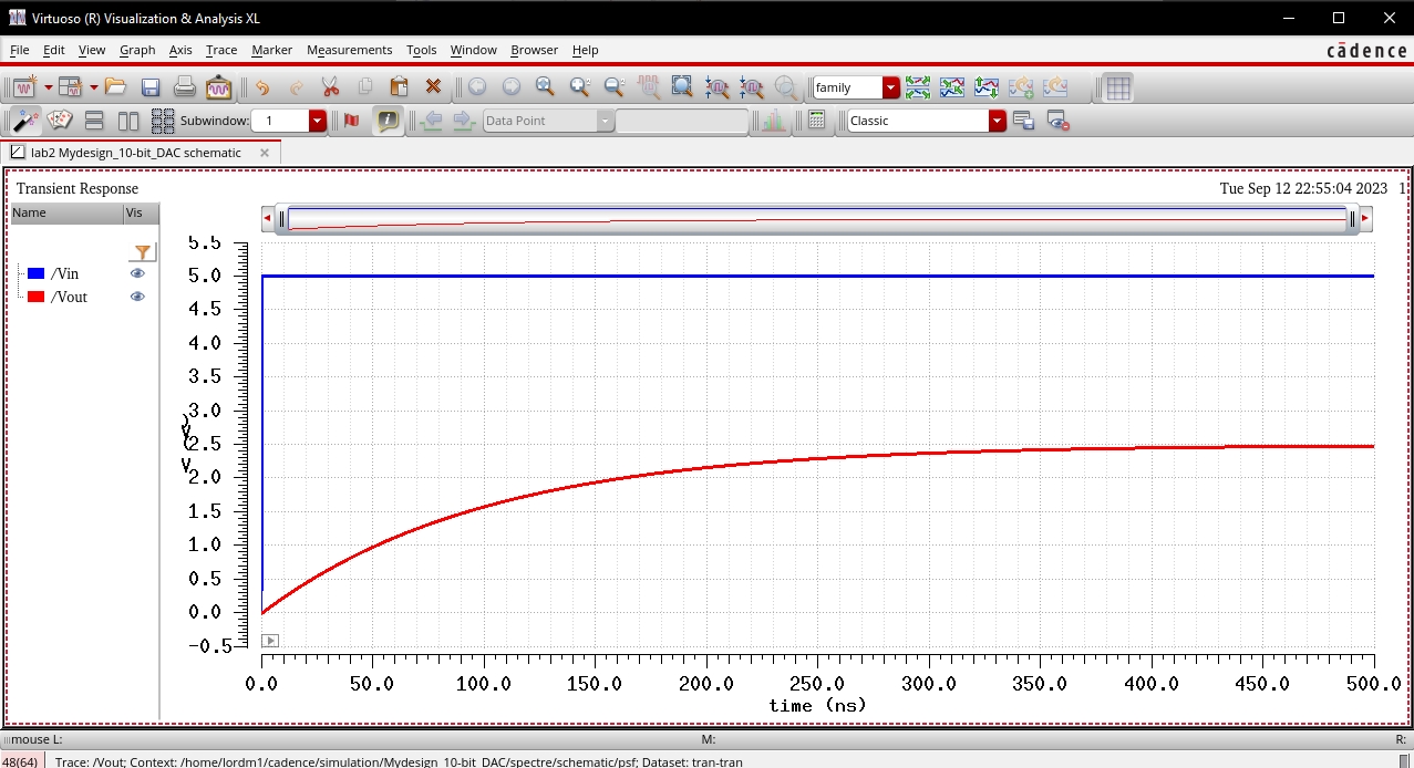
Determining Delay
Using the below equation we will solve for the time delay.
delay = 0.7RC
delay = 0.7(10k)(10p)
delay = 70ns
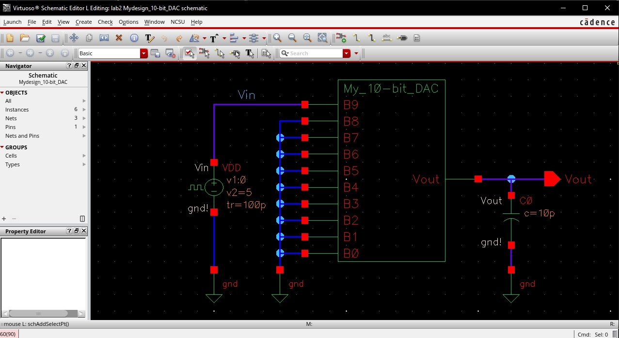
I grounded all bits of the DAC besides B9 and connected a pulse source to B9 in order to find the delay. In addition, a 10pF capacitor was introduced as the load.
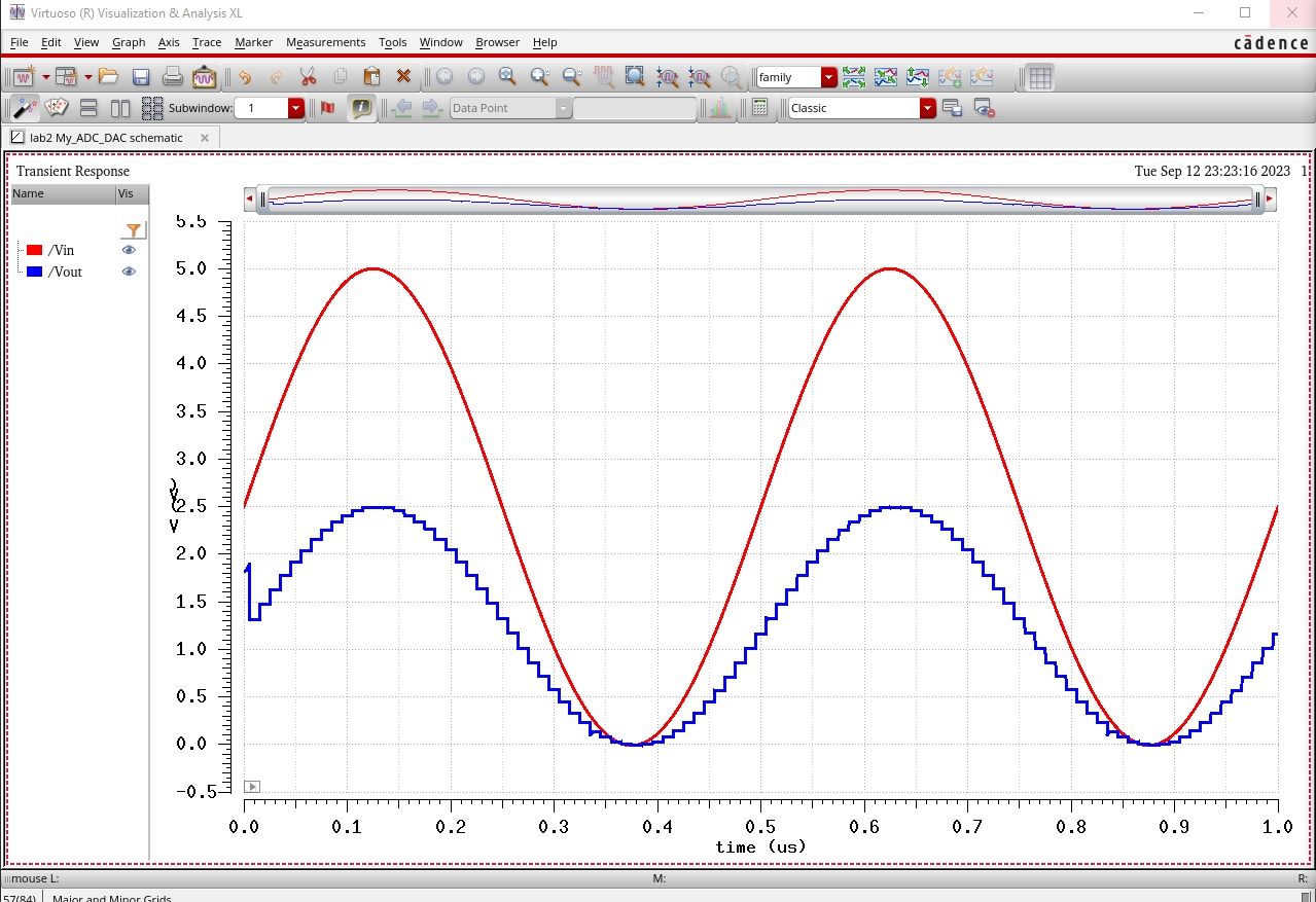
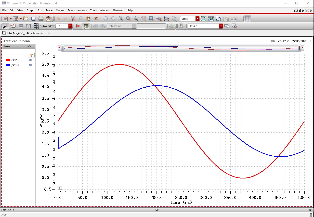
Verifying the validity of the Design
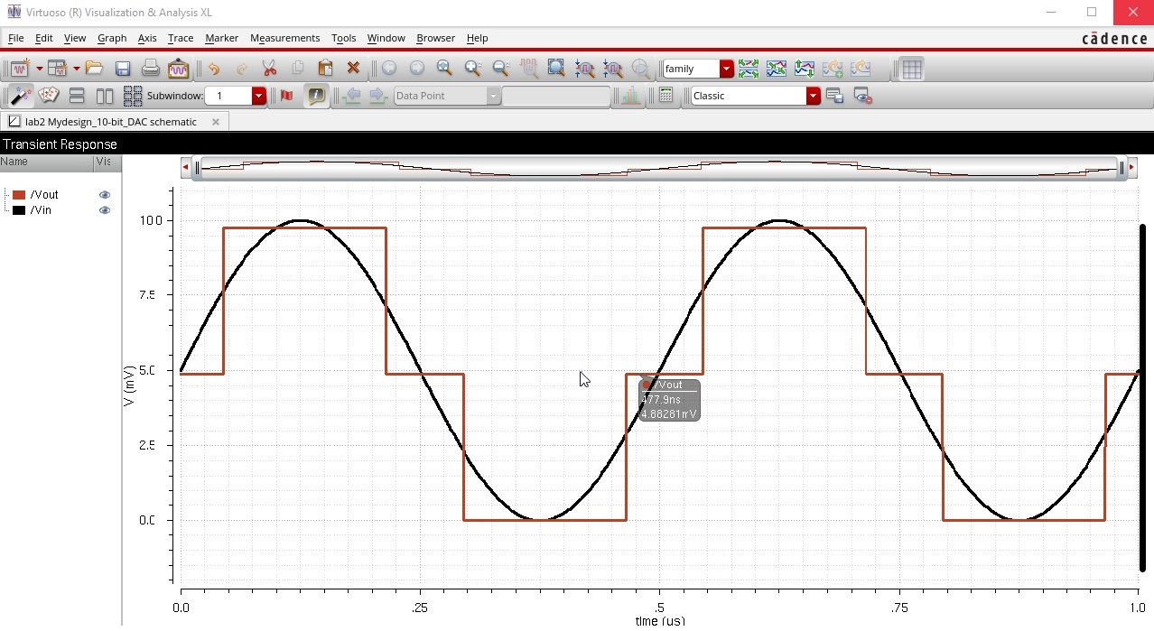
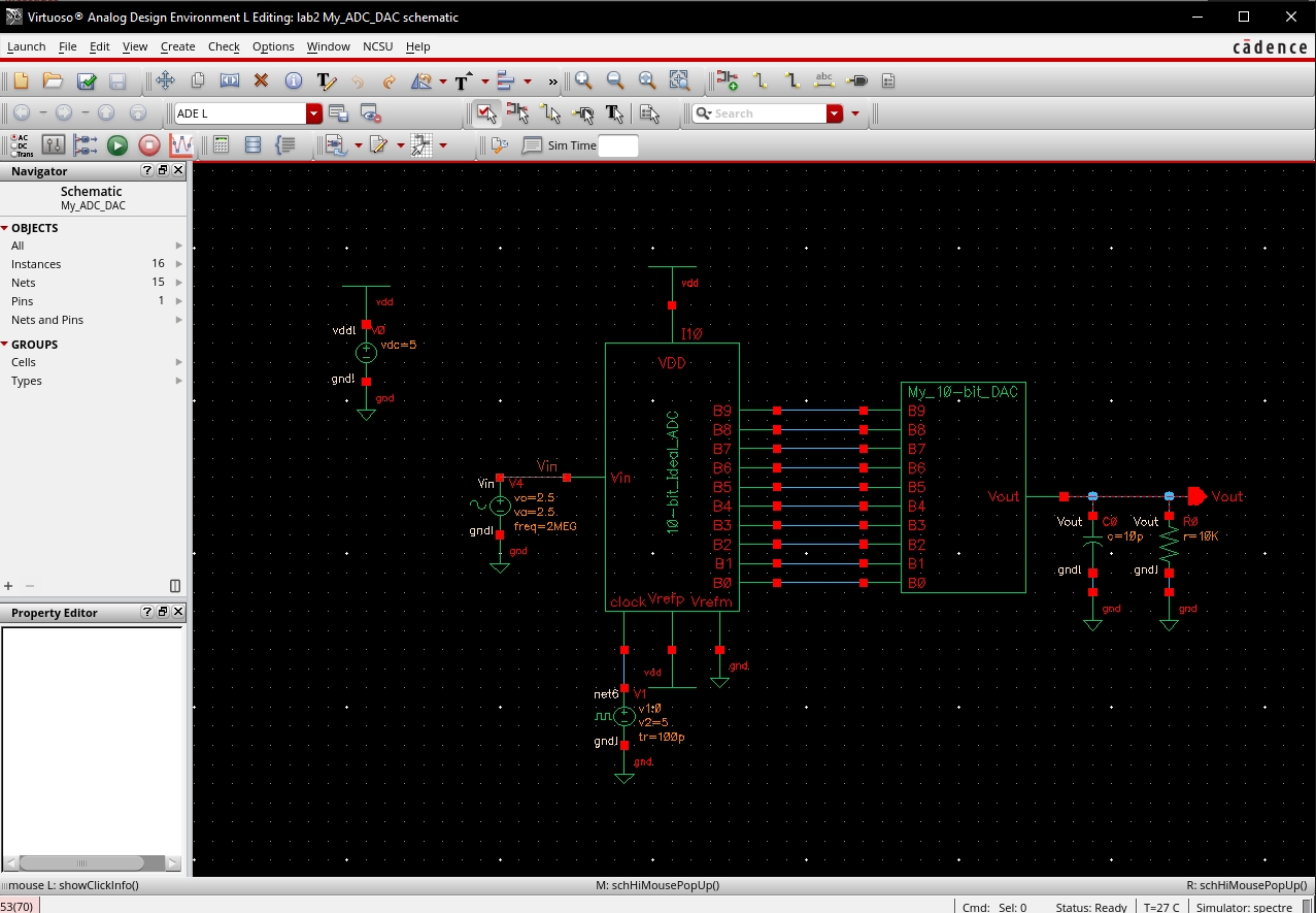
For us to verify our created DAC is working correctly we will be swapping out the ideal 10-bit DAC for the one modeled off of Figure 30.14.
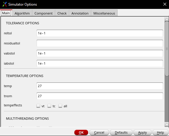
I did have issues with convergence errors so I ended up having to change the tolerance options in the ADE by clicking Simulation -> Options -> Analog and cchanging the values to those in the picture below.
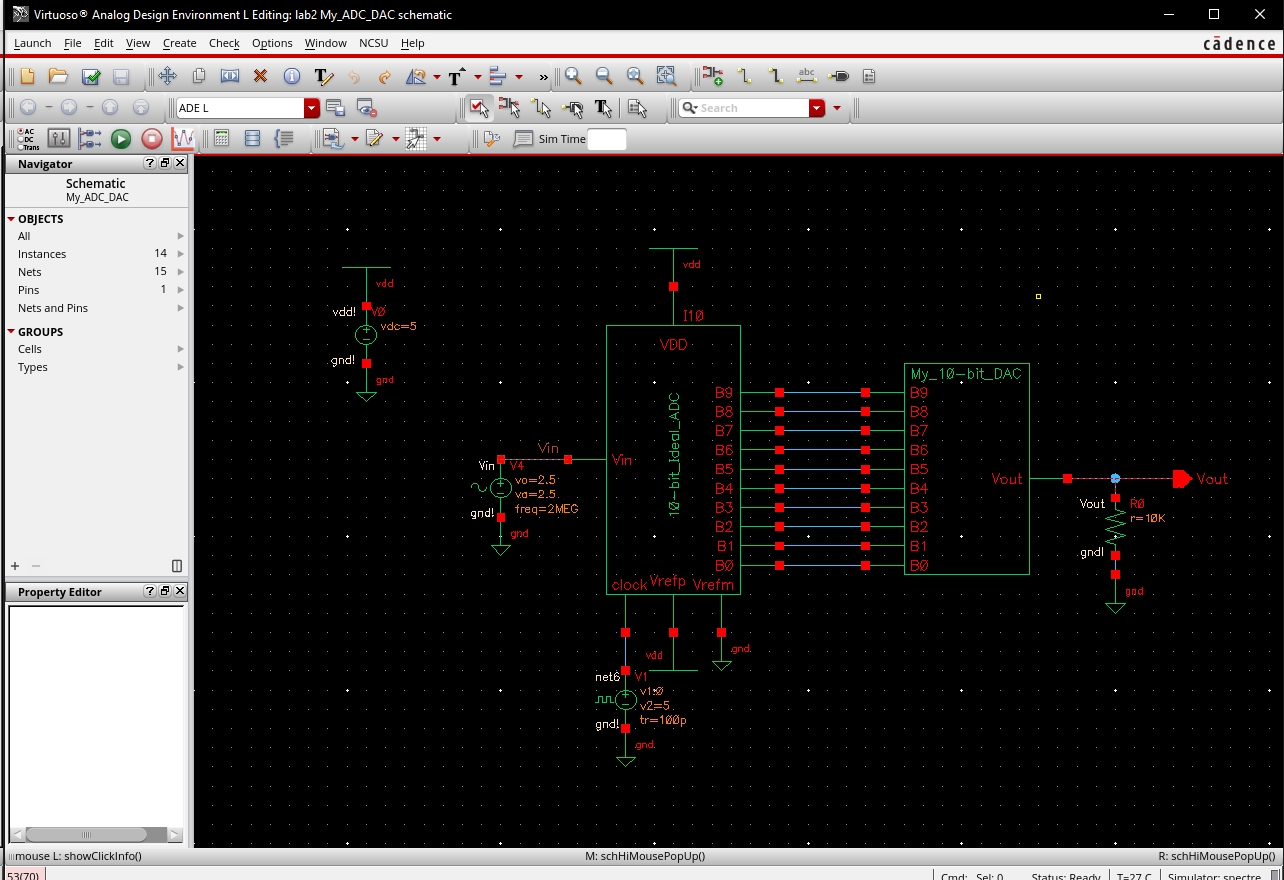
Introducing a Load to the DAC
First, I added a simulated load of with a 10k ohm resistor, cauing Vout to be halved.
With the output resistance of the DAC being 10k as well this is to be expected.
MOSFET Discussion
In an analog-to-digital converter (ADC) circuit, the switches that connect or disconnect various circuit elements are often implemented using transistors like MOSFETs. The resistance of these switches, often referred to as the "on-resistance" when the switch is in the closed (on) state, can have significant implications on the performance of the ADC if it is not small compared to the resistance of other elements in the circuit. Below are some of the theoretical consequences:
If the on-resistance is significant compared to , then it forms a voltage divider with . This can distort the analog signal being sampled, affecting the accuracy of the ADC.
High switch resistance combined with parasitic capacitances in the circuit could increase the RC time constant. This means that the signal would take longer to settle, potentially requiring a slower sampling rate for accurate conversions.
Higher resistance usually translates to higher thermal noise, which can degrade the signal-to-noise ratio (SNR) of the ADC.
Although this is usually a minor concern, higher resistance will consume more power, which might be a crucial factor in low-power applications.
The variable switch resistance could introduce nonlinearities in the ADC conversion process, making it difficult to achieve a linear response.
An elevated switch resistance could reduce the effective dynamic range of the ADC, as the signal might be attenuated before it reaches the sampling circuit.
Given these issues, careful design and selection of the transistors used as switches are crucial for ADC performance. In some cases, calibration or compensation techniques may be employed to mitigate the effects of significant switch resistance.