Lab 7 - EE 421L
Authored
by Anthony Lopez
Email: lopeza78@unlv.nevada.edu
Due Date: November 8, 2023
Lab Description:
- Main objectives
- Develop the layout and schematic for a ring oscilator.
- Develop the schematic and symbol for a 4 bit word inverter.
- Develop schematics and symbols for an 8-bit input/output array of: NAND, NOR, AND, inverter, and OR gates.
- Develop the schematic and symbol for a 2 to 1 DEMUX/MUX and an 8 bit wide word 2 to 1 DEMUX/MUX.
- Develop a schematic and symbol for a full adder to then be used for an 8-bit adder schematic and symbol.
- Simulate our designs in a example circuits.
Pre-Lab:
- Back-up all of your previous work from the lab and the course.
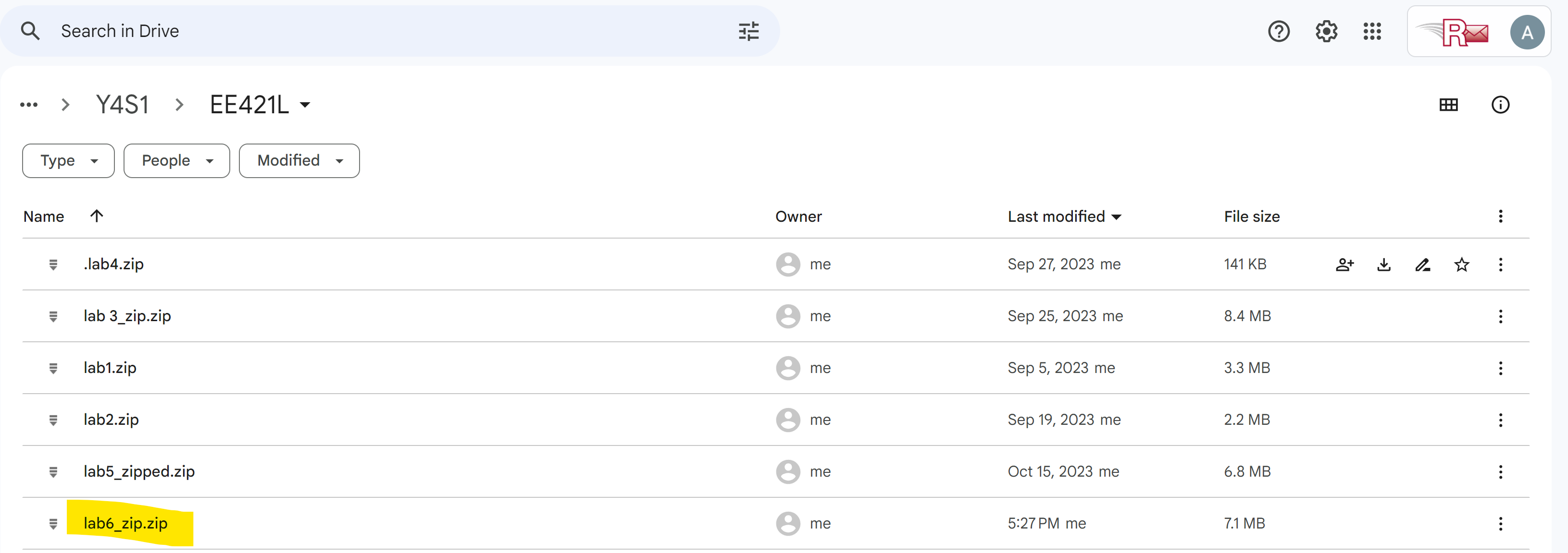
- The following shows my zipped lab 6 file in my drive.
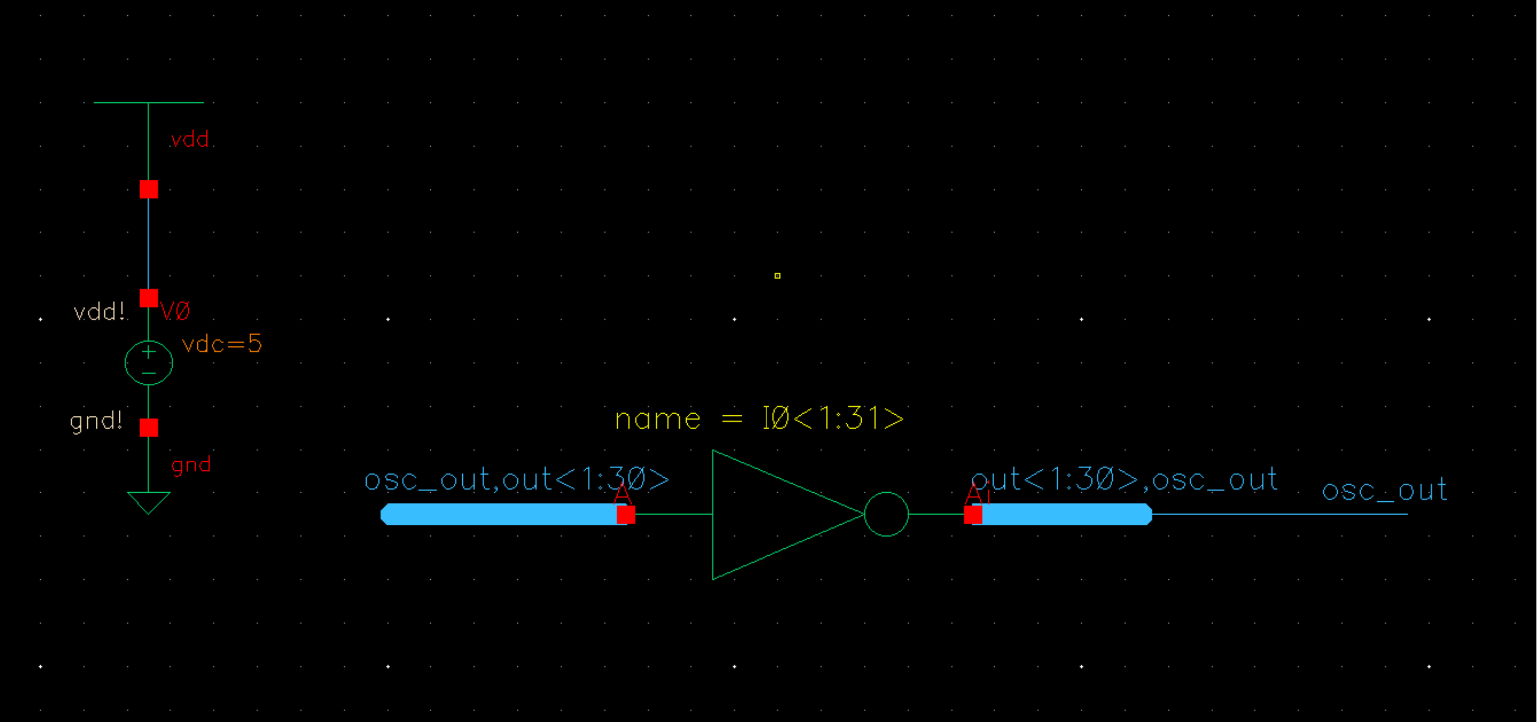
- The following is my initial developed schematic for the ring oscillator.
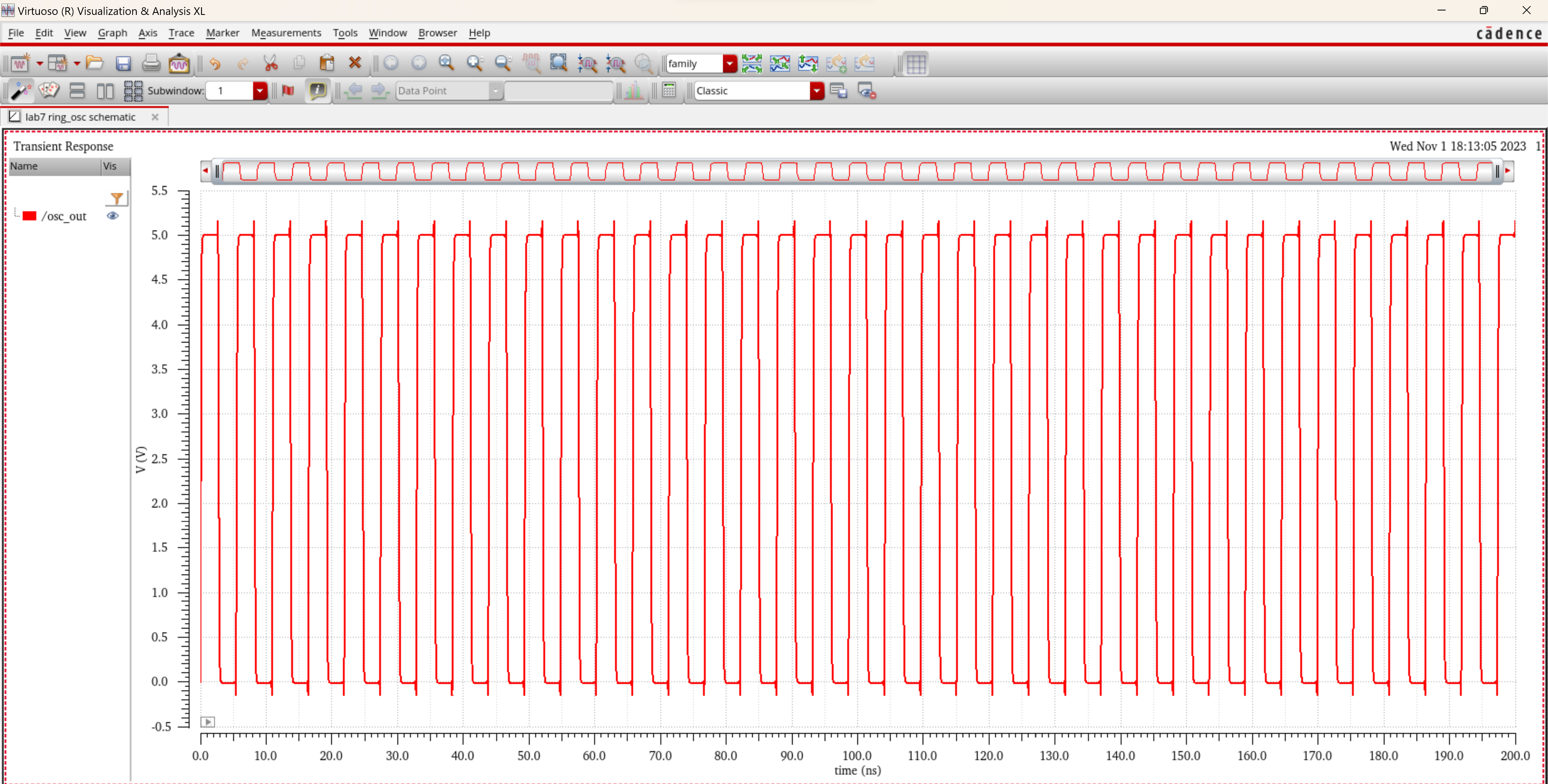
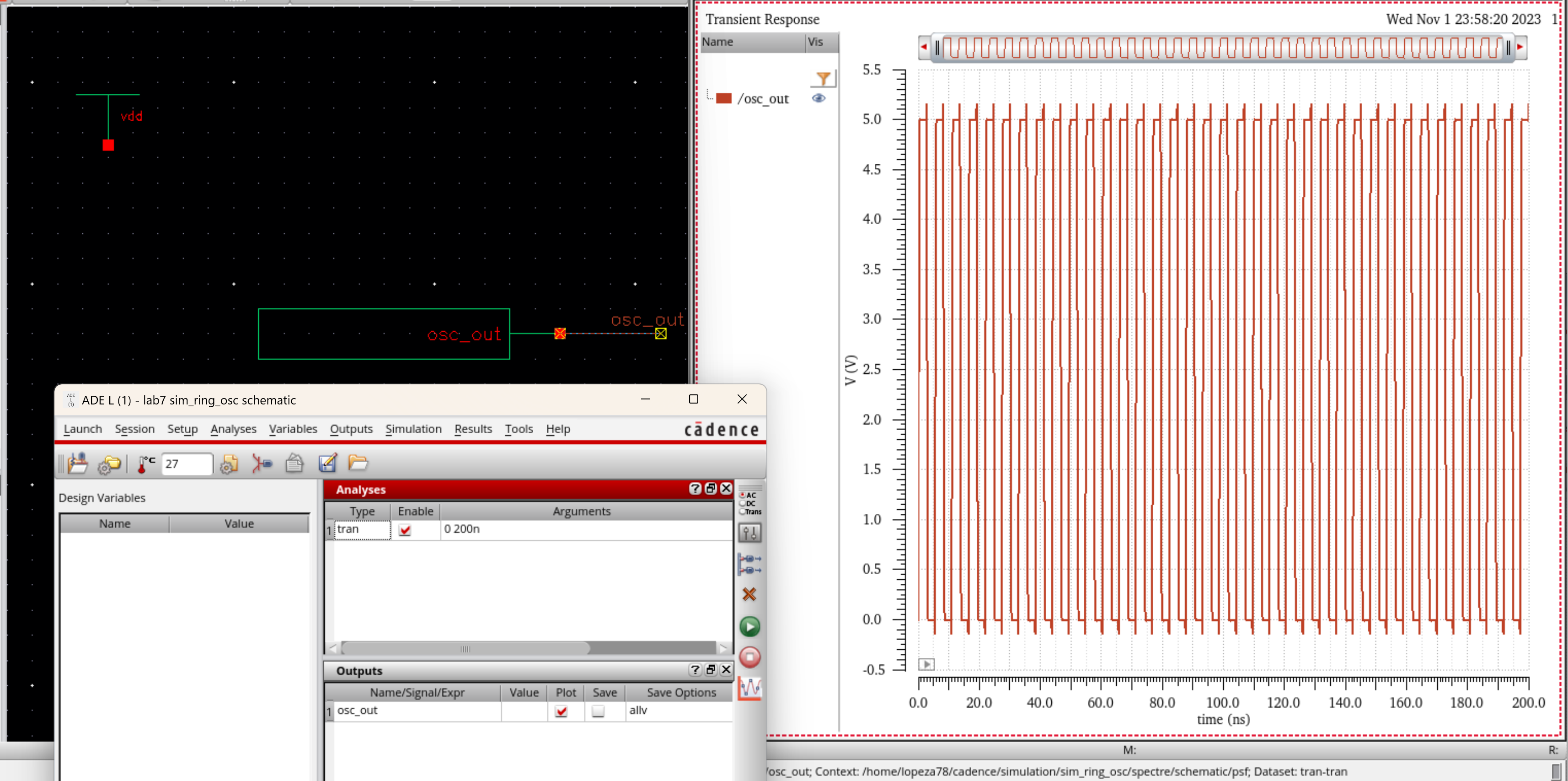
- Now we simulate and observe the output node of osc_out.
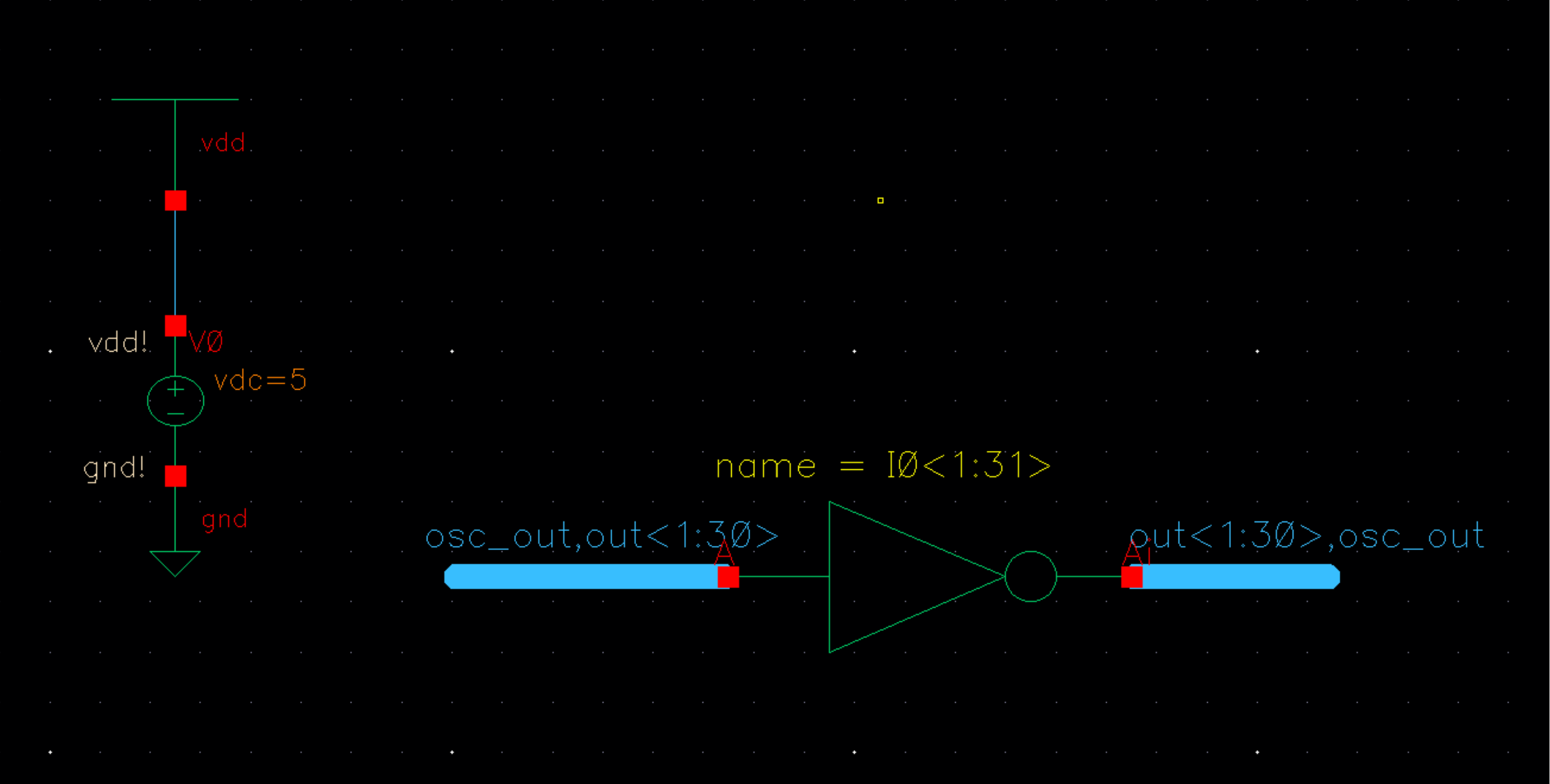
- Continuing
the tutorial we will now develop a proper schematic using arrays and
buses. There is no need to resimulate since it is the same schematic
just more compact and neat.
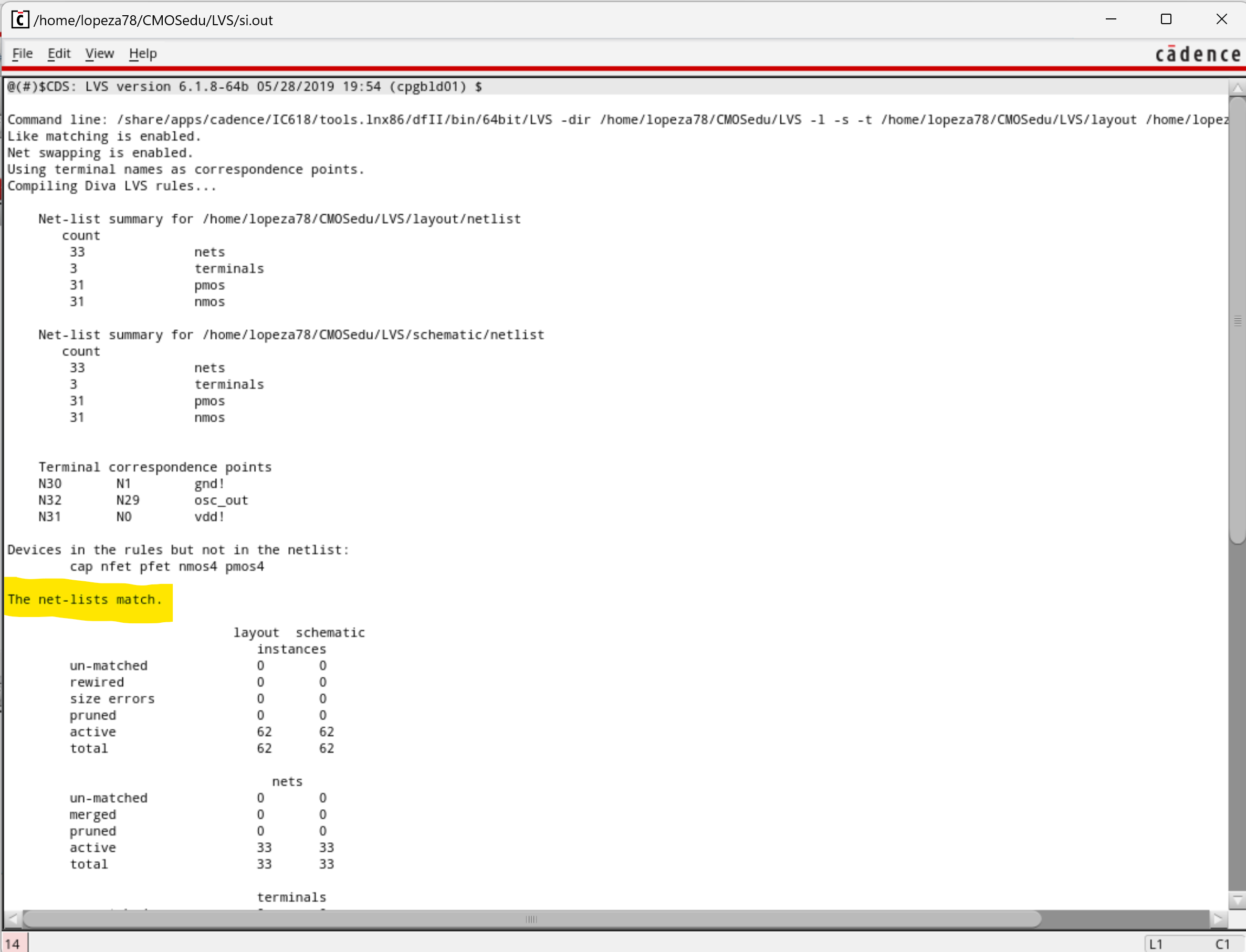
- Now
the following is the LVS compared to the schematic previously shown.
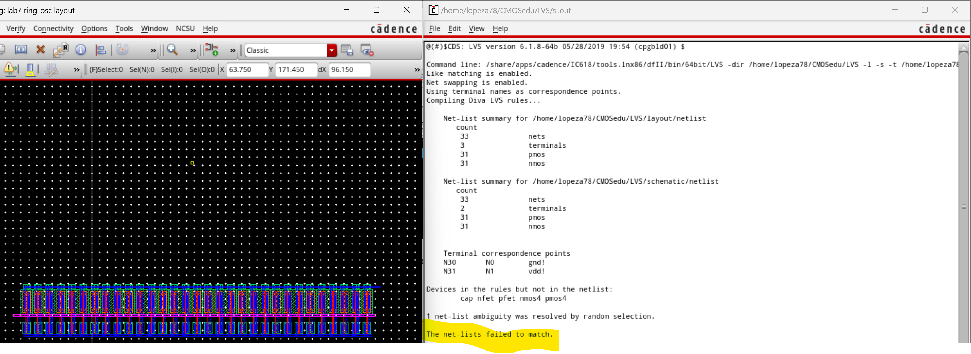
- However
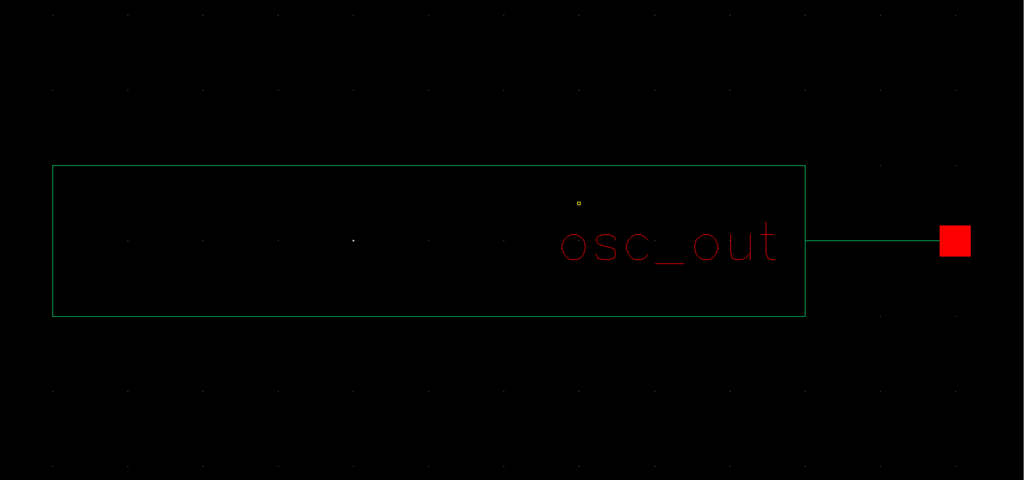
this LVS fails due to our schematic thus we make the following changes
and LVS again. (First image is the new schematic then the LVS results.)
- Now we develop a symbol and sim schematic with its results.
-This concludes our prelab.
Lab Tasks:
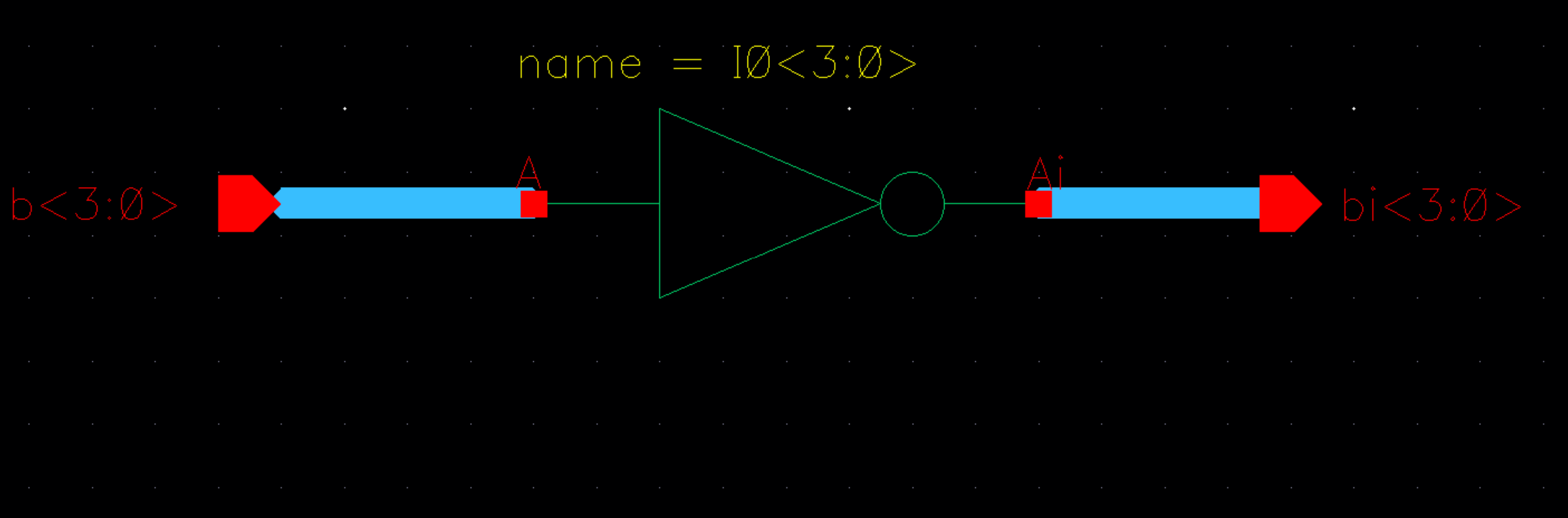
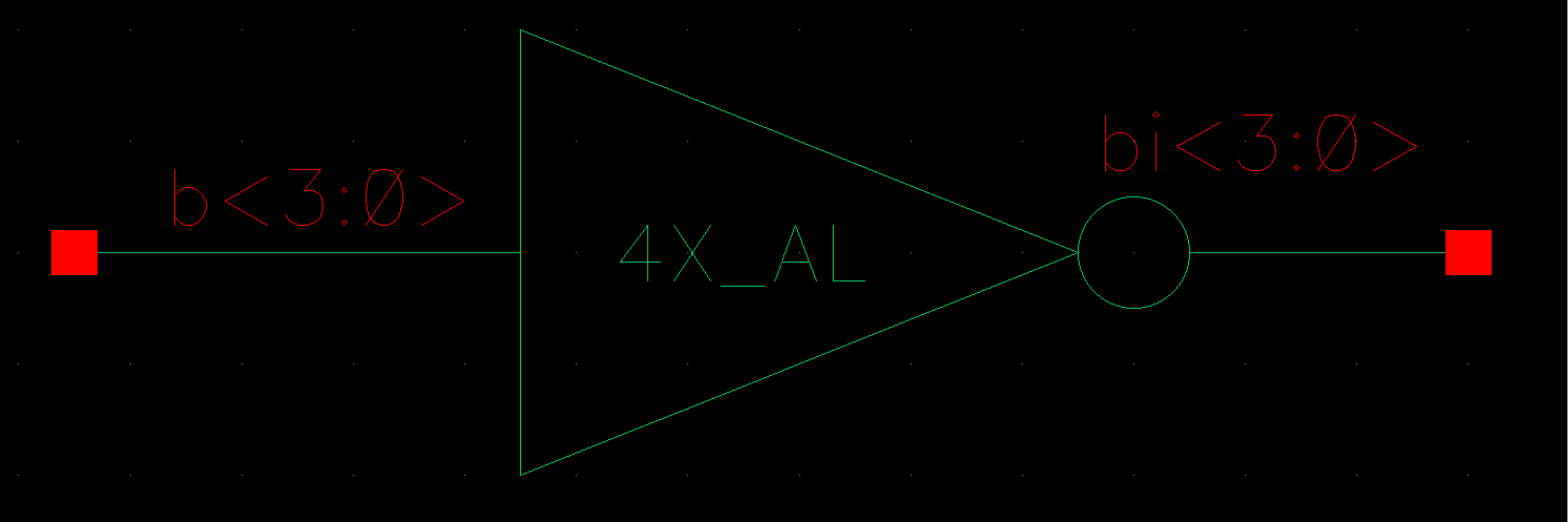
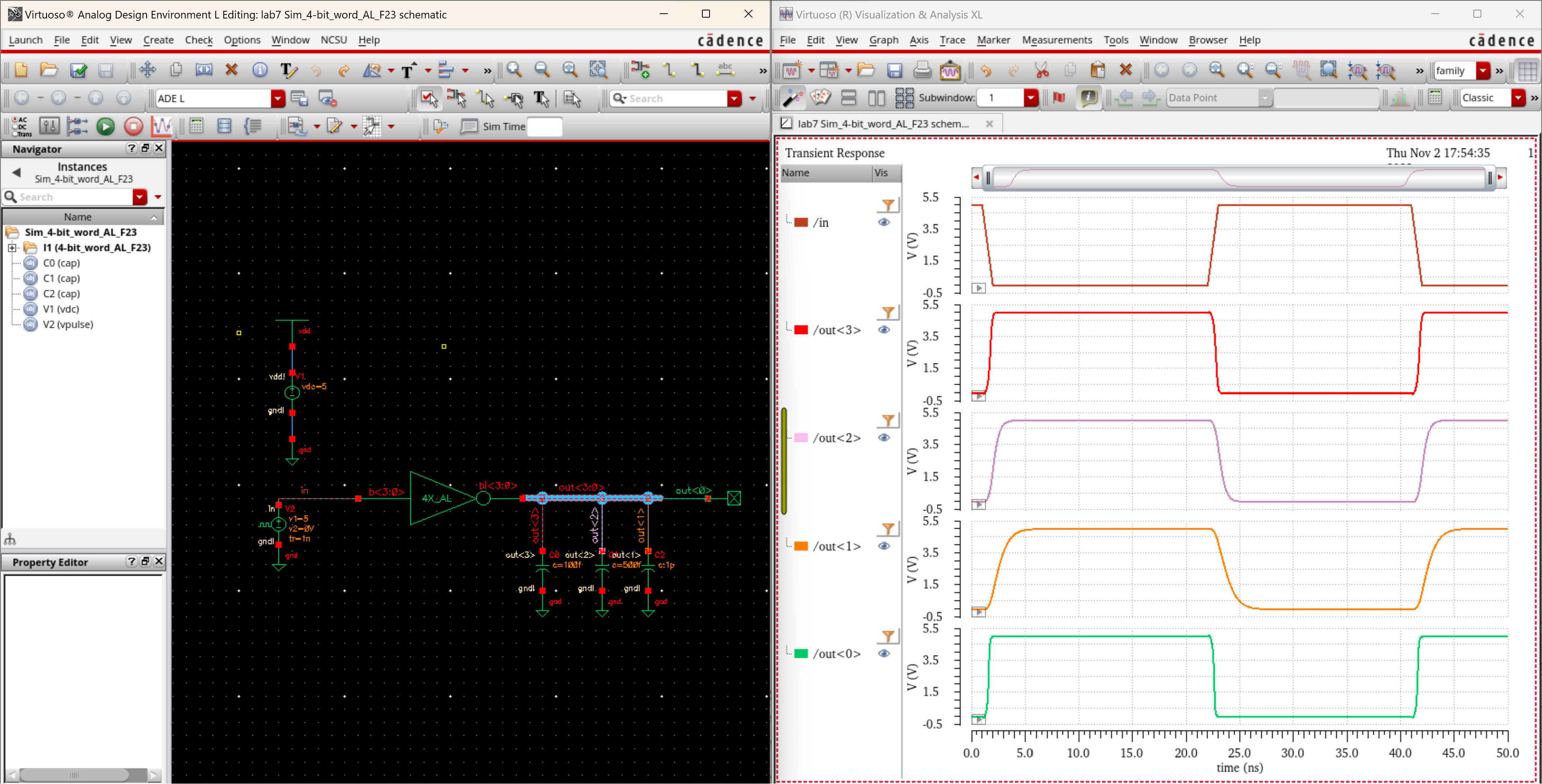
- The schematic, symbol, and simulation for a 4 bit word inverter.
- Simulation
schematic and results. From these results you can see that the higher
the capacitive load the smoother the rise and fall times. Not only this
but much less of a delay.
- Develop schematics and symbols for an 8-bit input/output array of: NAND, NOR, AND, inverter, and OR gates.
- Note all of my gate instances that build these new 8-bit arrays come from lab 6 and 5.
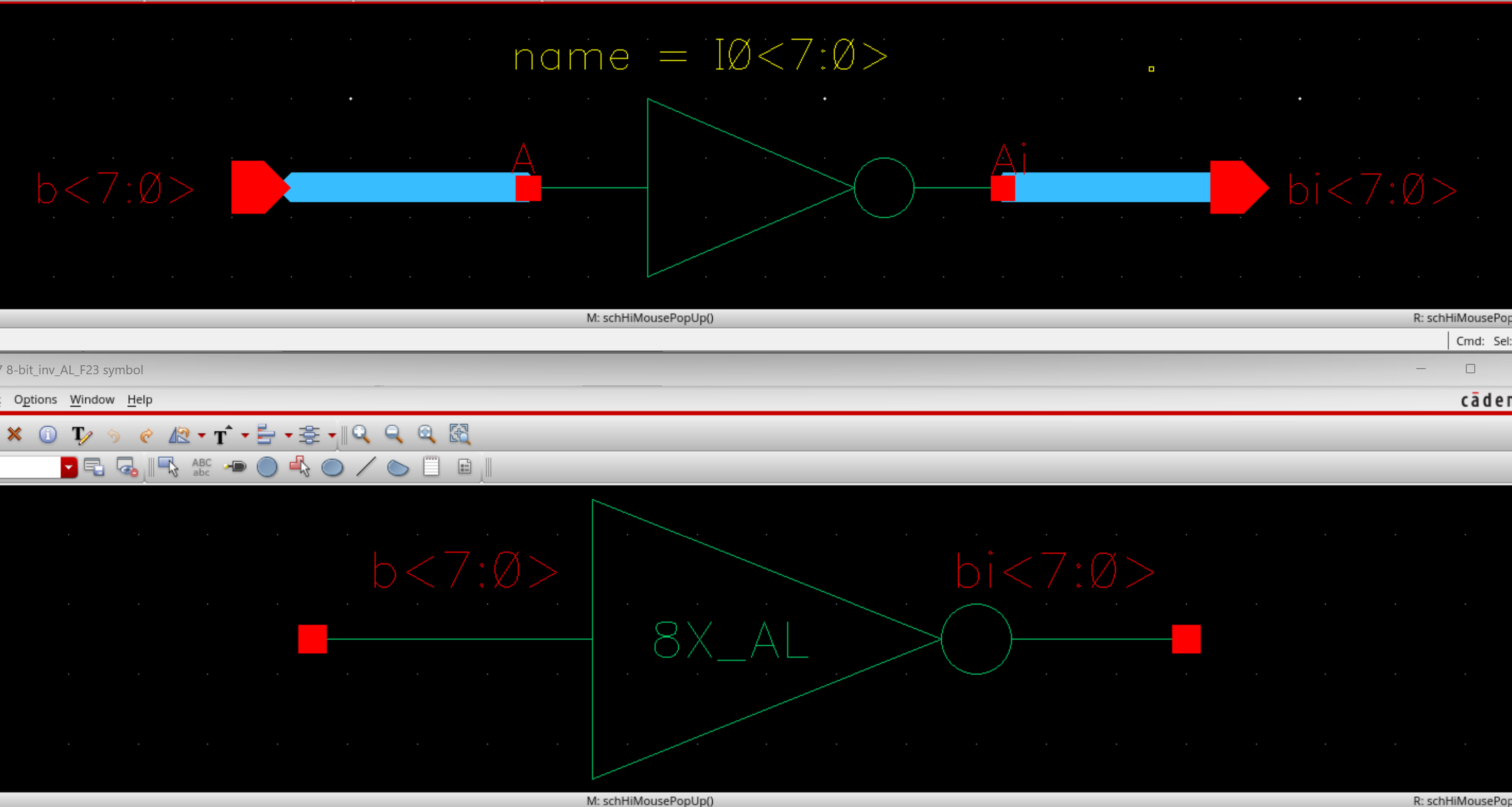
- The schematic and symbol for the 8-bit inverter.
- The schematic and symbol for the 8-bit NAND.
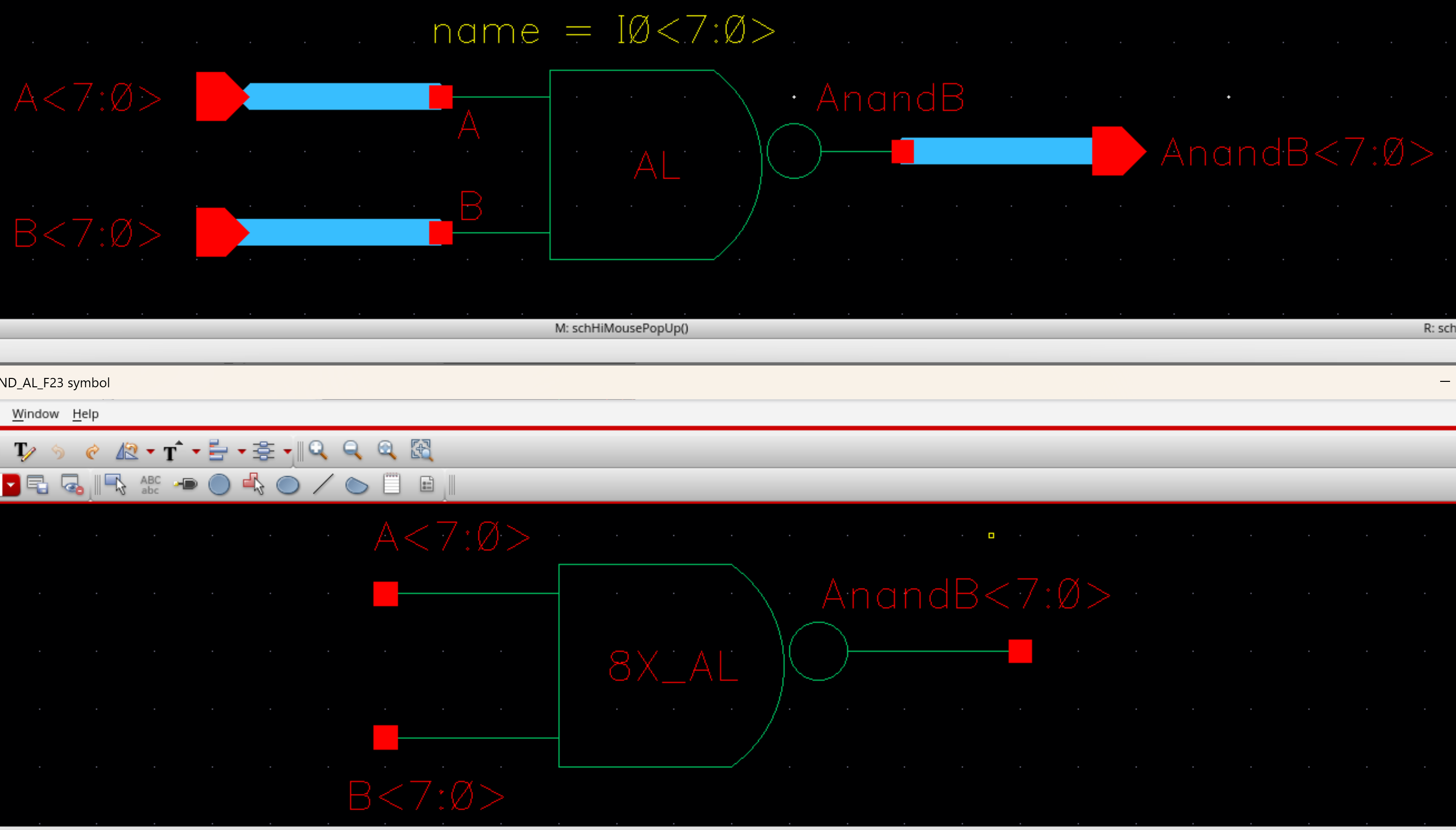
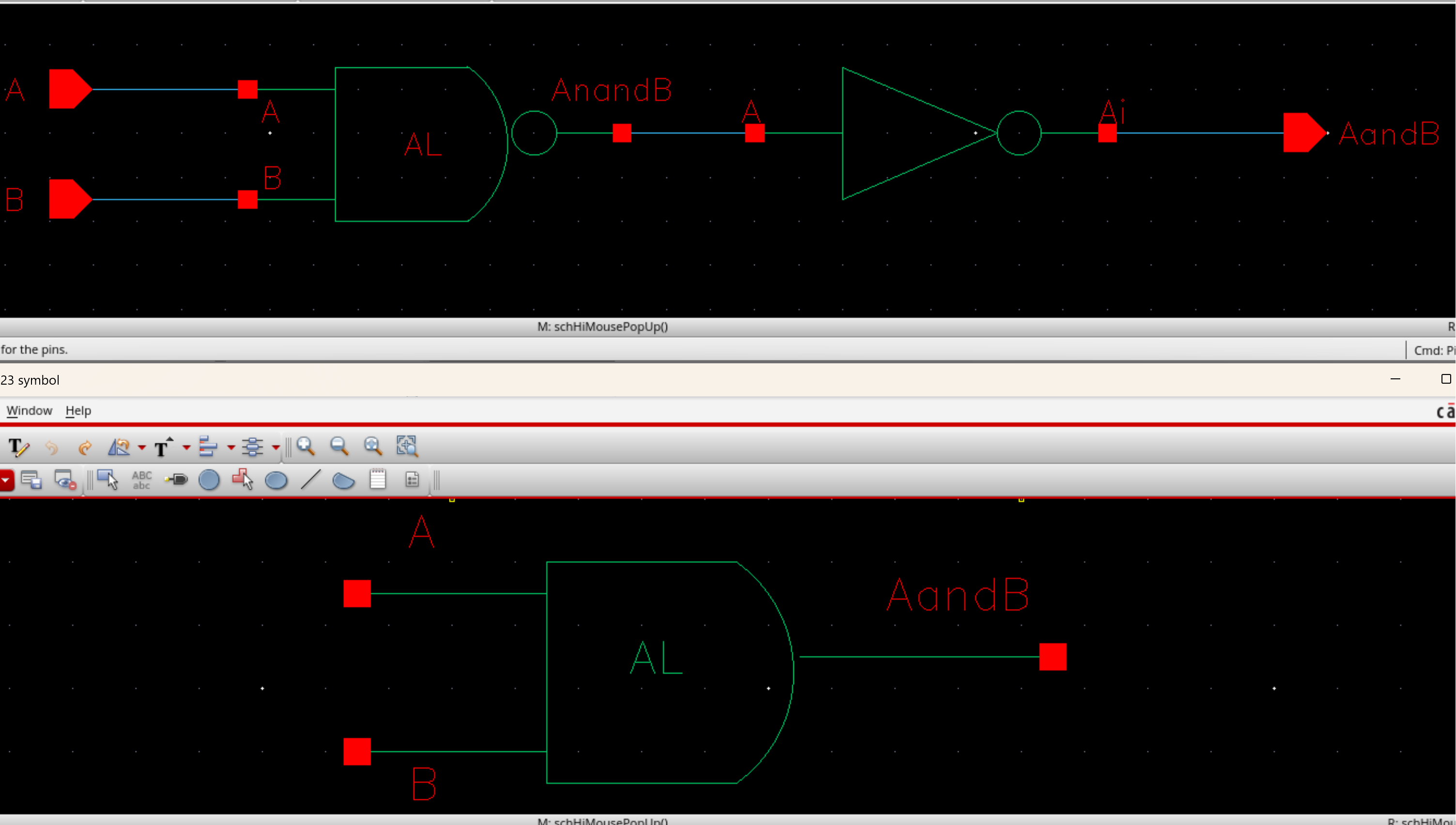
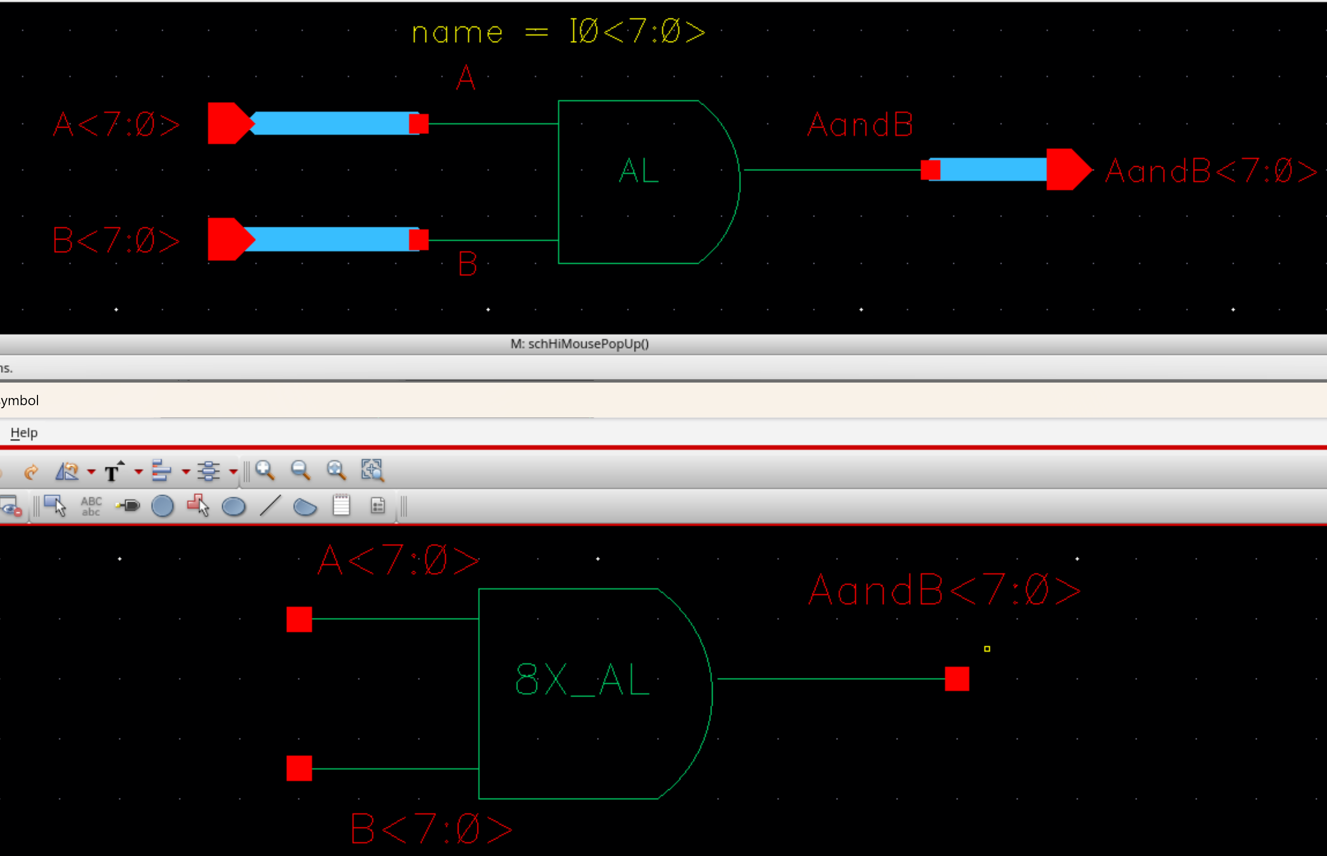
- The
schematic and symbol for the 8-bit AND. Since I do not have a
developed one bit AND gate, the first image is the schematic and symbol
for a one bit AND gate.
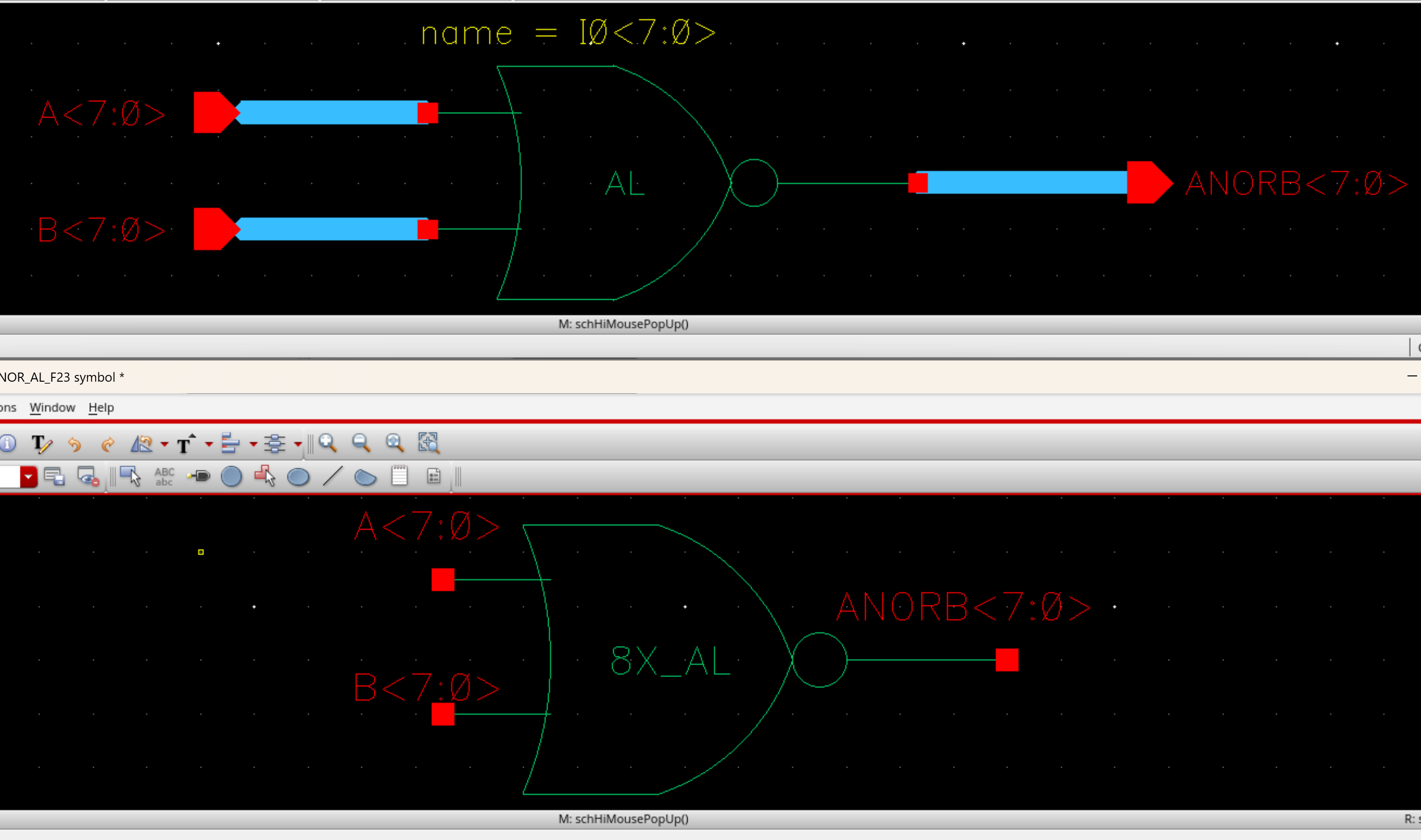
- The schematic and symbol for the 8-bit NOR.
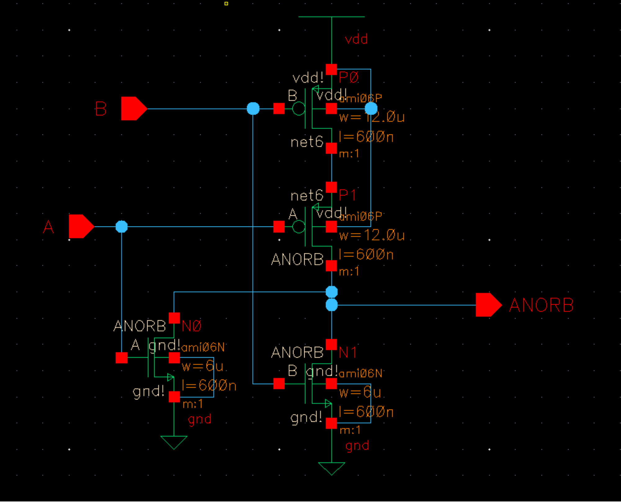
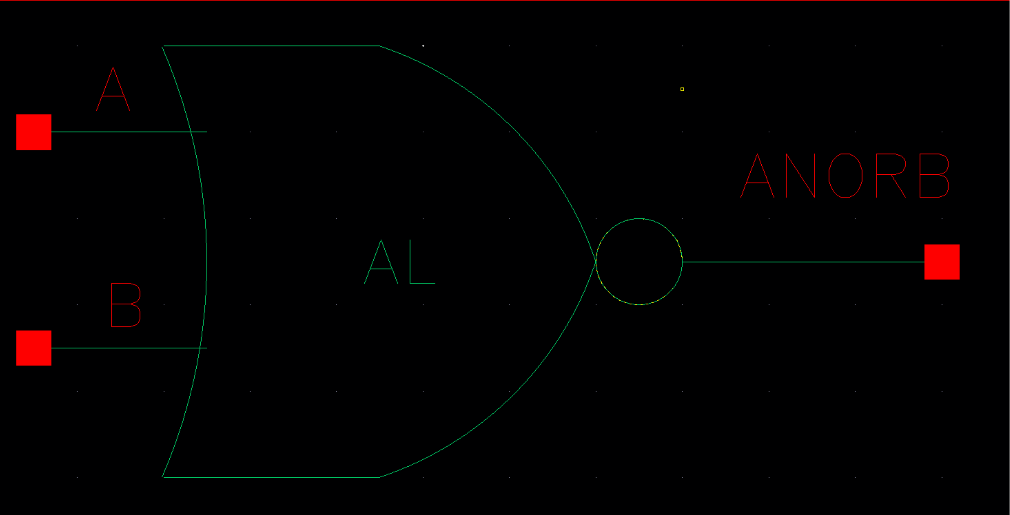
- First I must develop from stratch a Nor gate. Thus, the follwoing is the schematic and symbol for a simple Nor gate.
- Here we now have our 8-bit NOR schematic and symbol
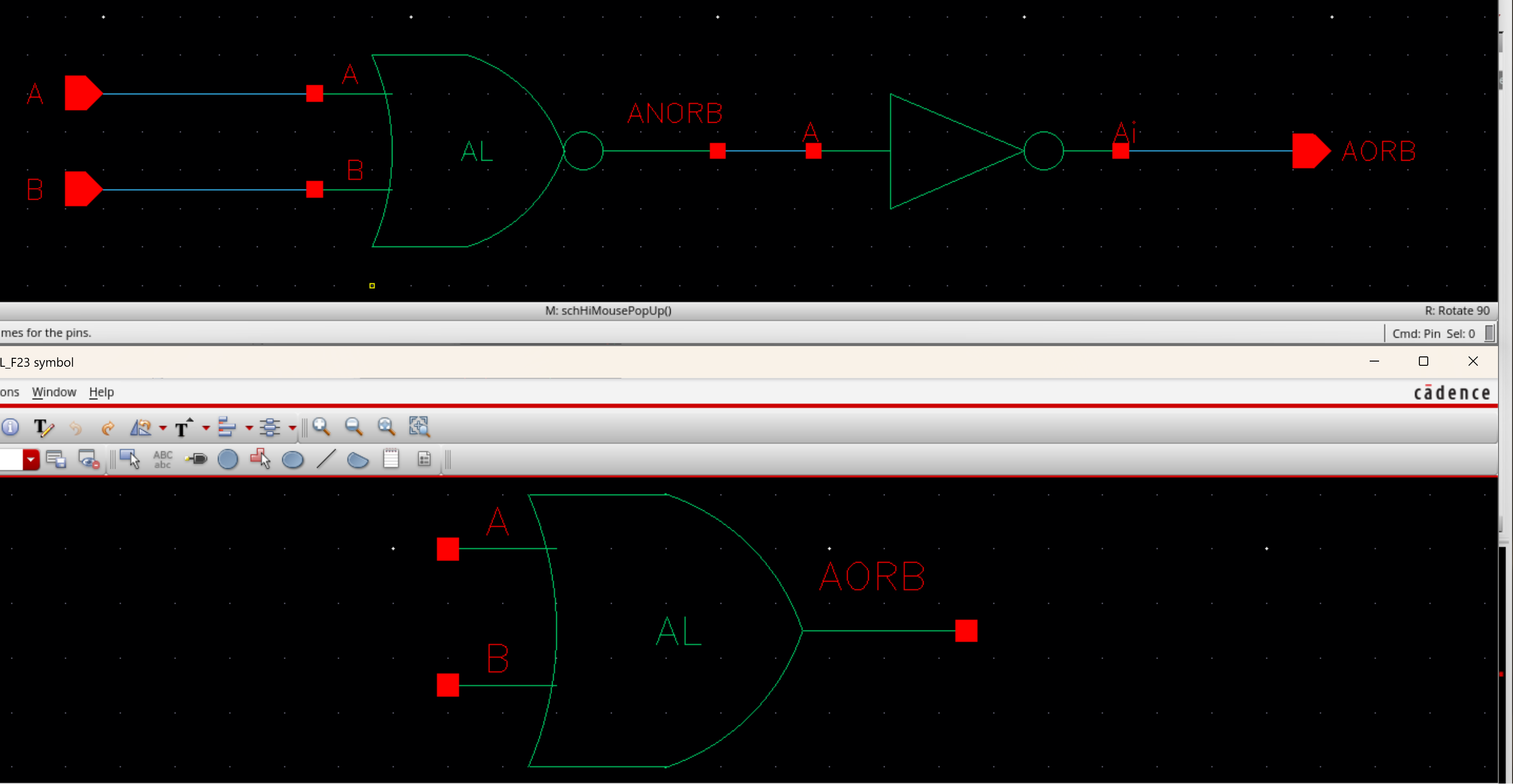
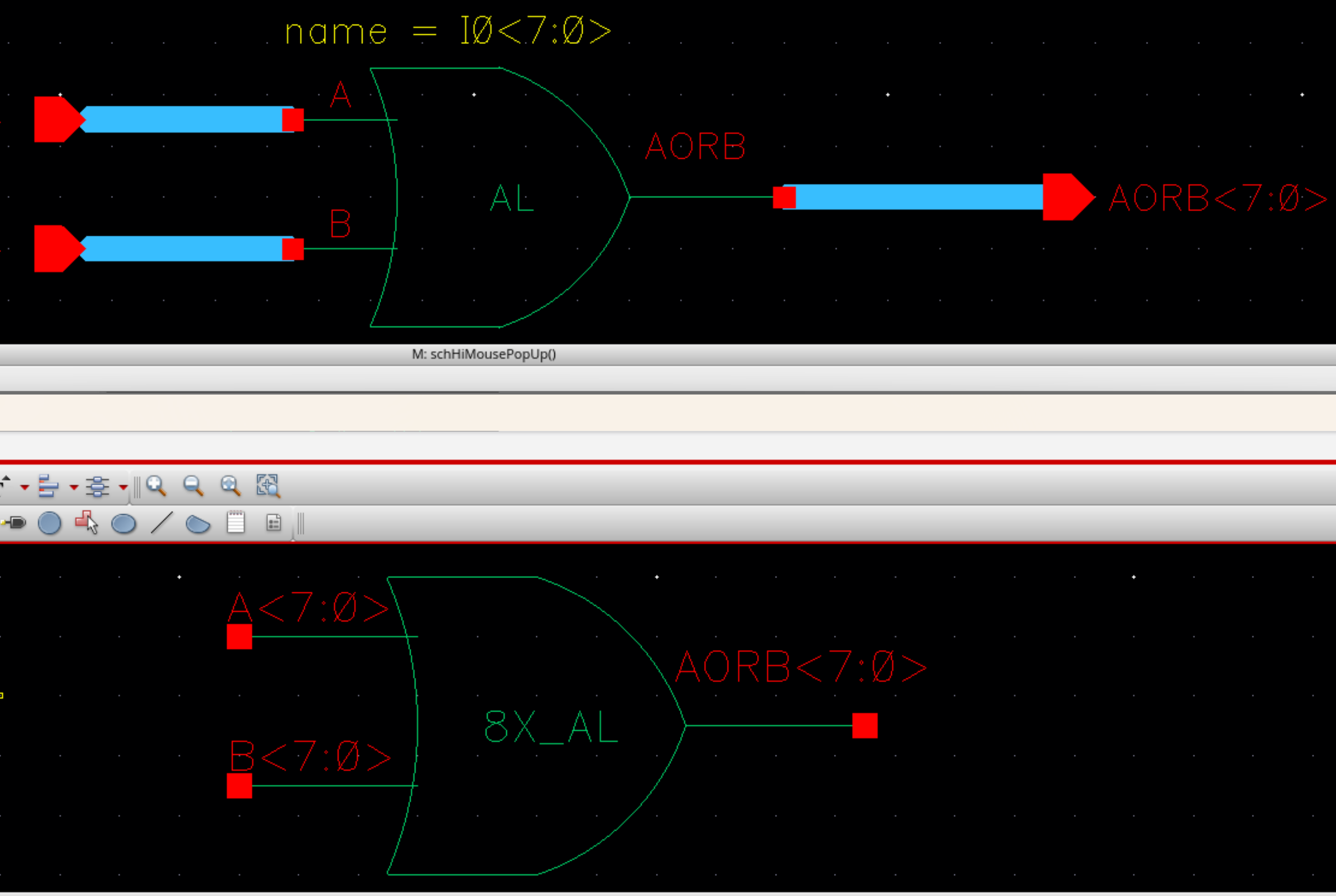
- The schematic and symbol for the one bit OR gate and 8-bit OR gate respectively.
- This section is a simulation of all of our 8 bit gates. In one simulation we display the 8 bit output of each gate.
- Develop the schematic and symbol for a 2 to 1 DEMUX/MUX and an 8 bit wide word 2 to 1 DEMUX/MUX.
- Develop a schematic and symbol for a full adder to then be used for an 8-bit adder schematic and symbol.
Return