Lab 6 - EE 421L
Authored
by Anthony Lopez
Email: lopeza78@unlv.nevada.edu
Due Date: October 25, 2023
Lab Description:
- Main objectives
- Develop 2 input NAND and XOR gate. Drafting its schematic, symbol and layout.
- Develop a full adder. Drafting a schematic, symbol and layout.
- Simulate our designs in a example circuits.
Pre-Lab:
- Back-up all of your previous work from the lab and the course.
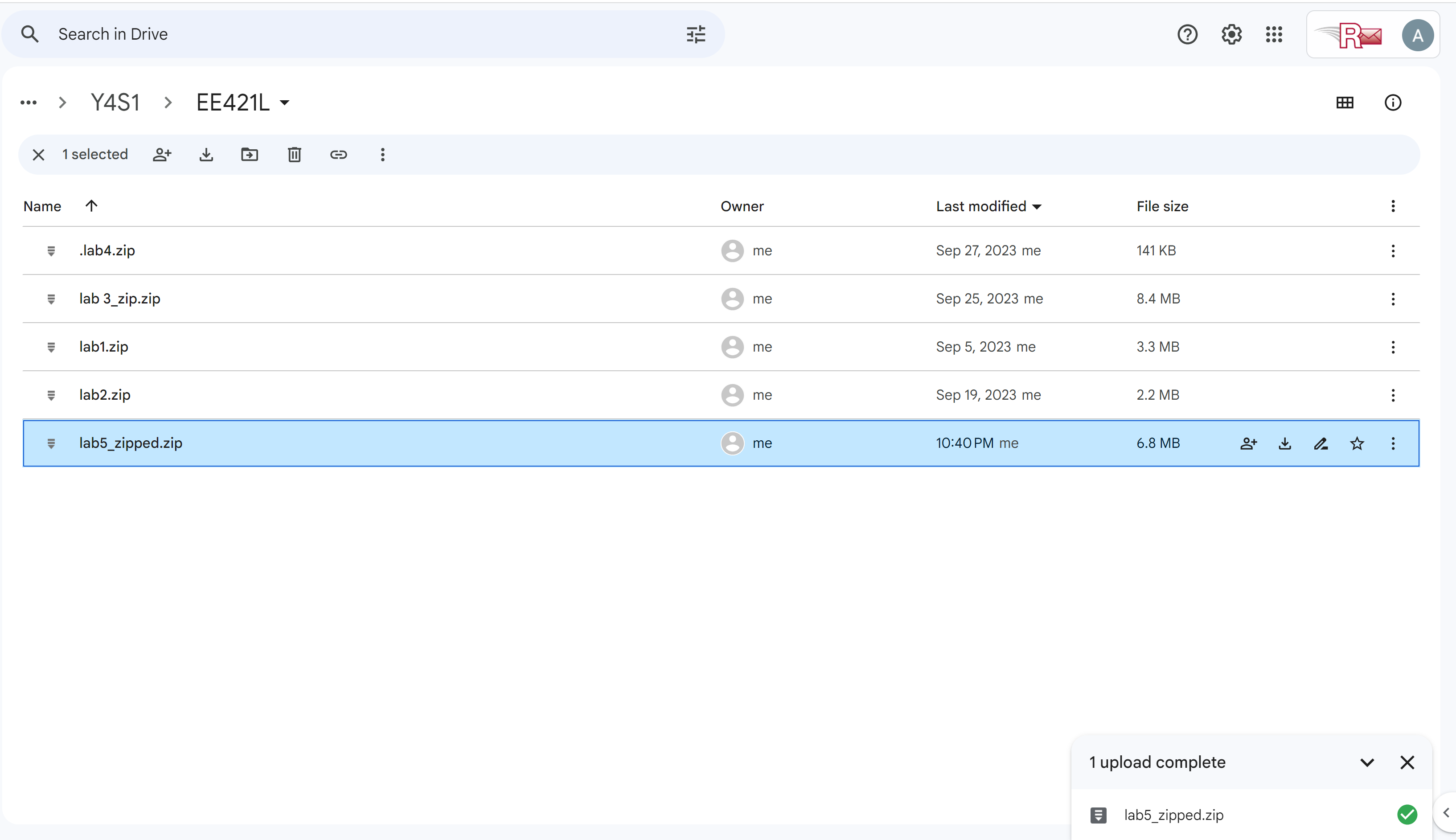
- The following shows my zipped lab 6 file in my drive.
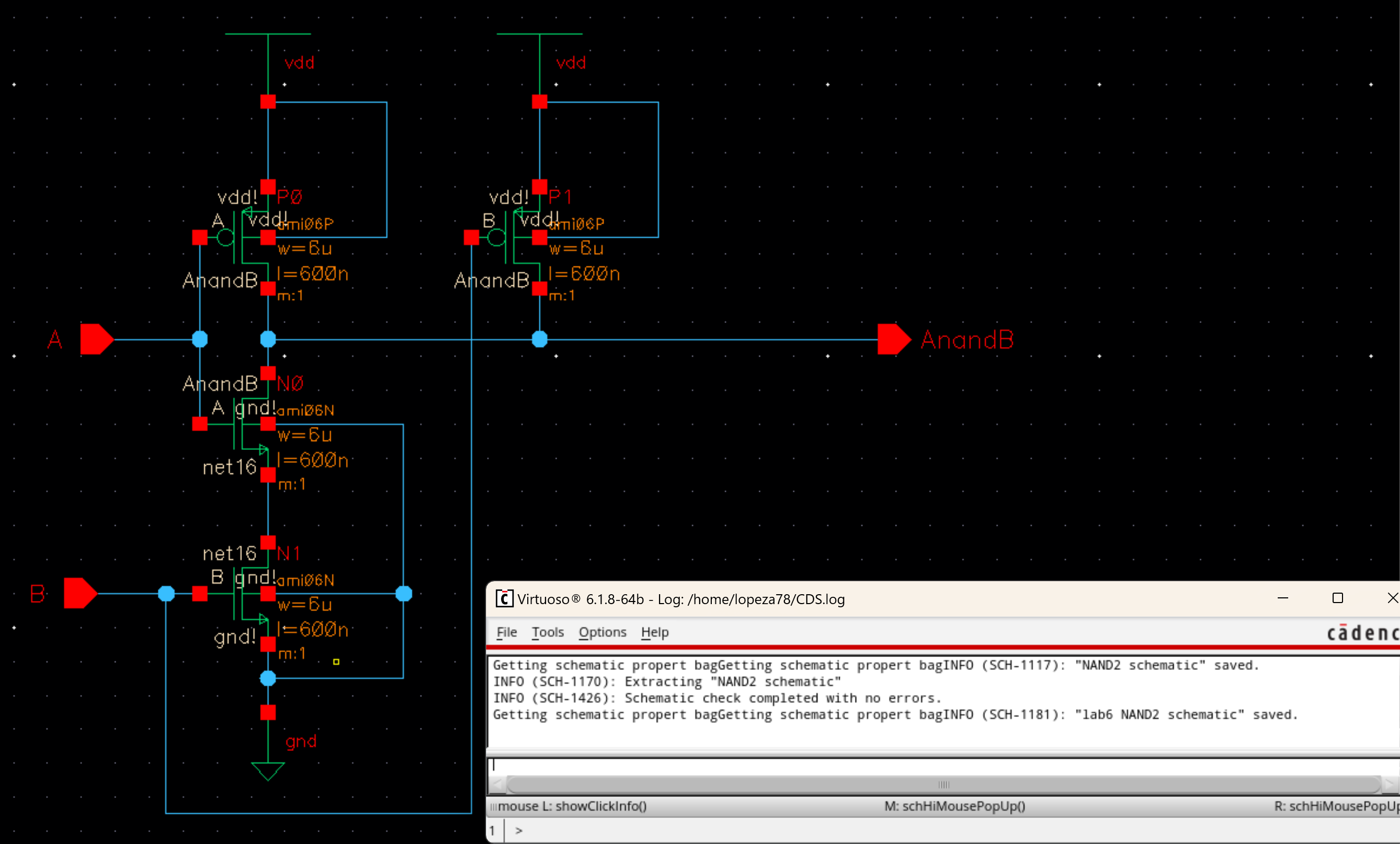
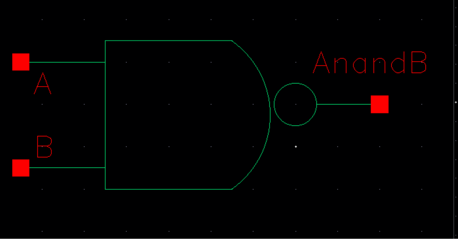
- The following is my developed schematic and symbol,respectively, for the 2 input NAND gate.
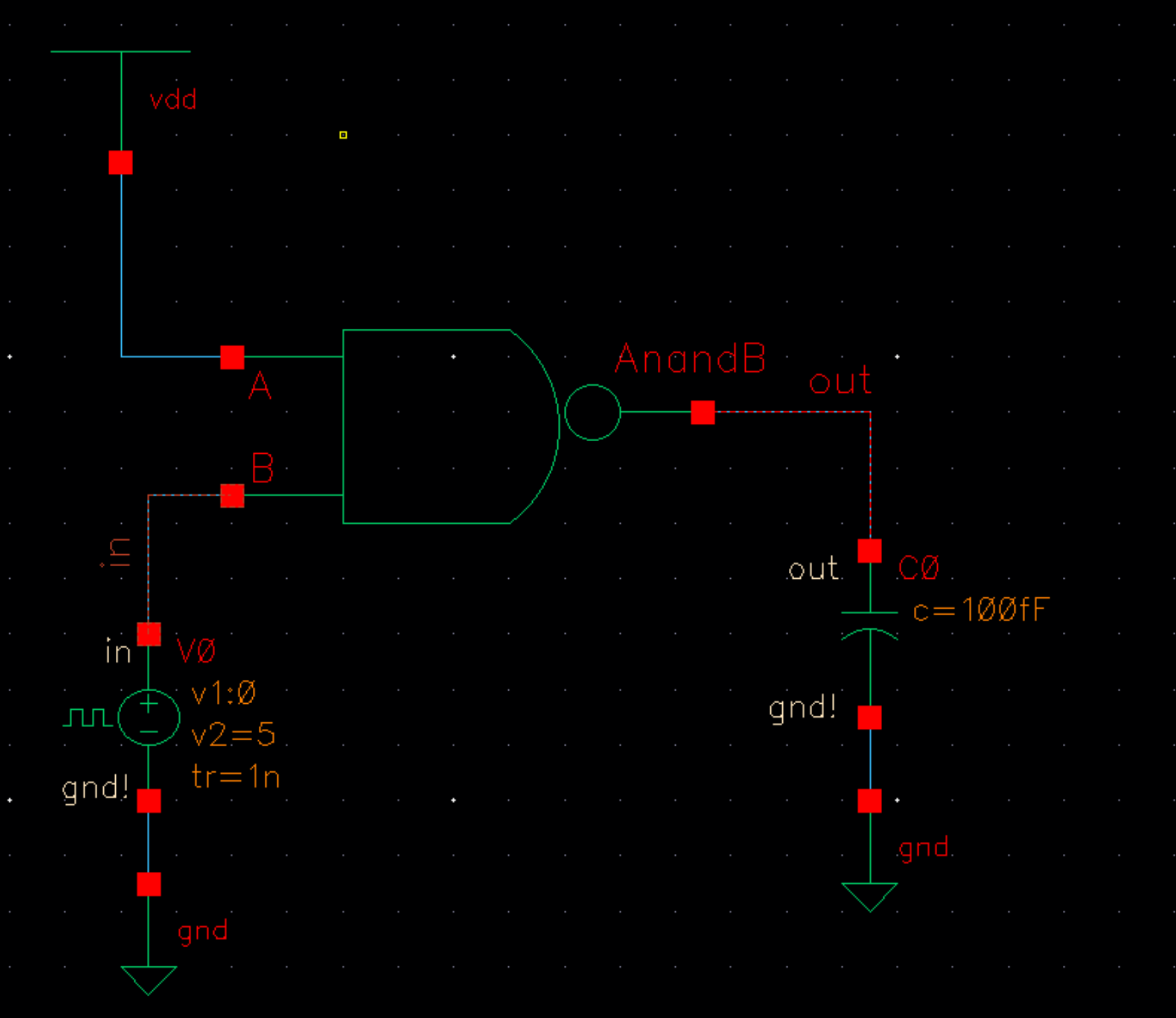
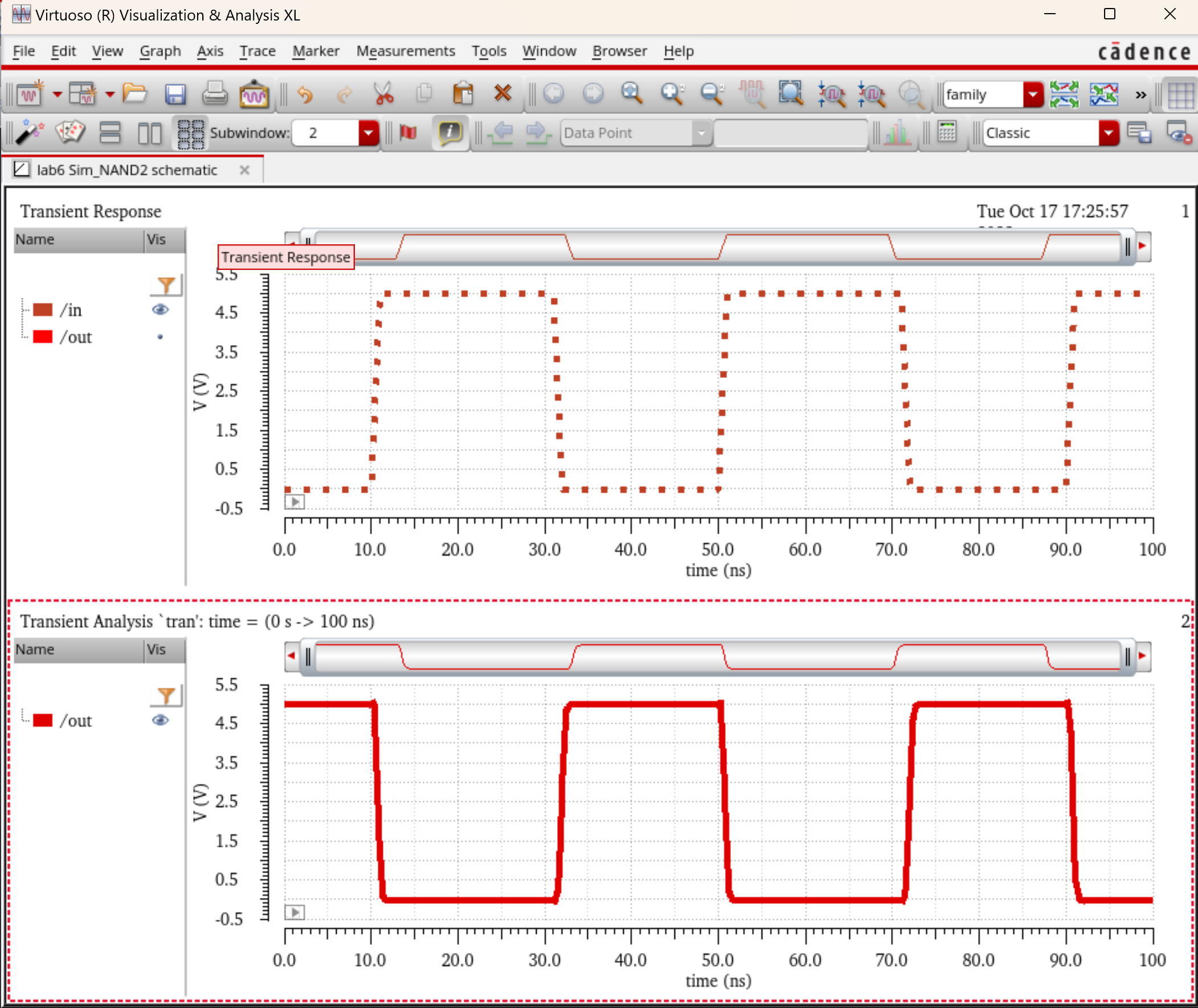
- Now we simulate. The first image is the schematic we will simulate then follows
the results of our dc sweep simulation, having V0 going from 0v to 5v
in increments of 1m.


- Continuing
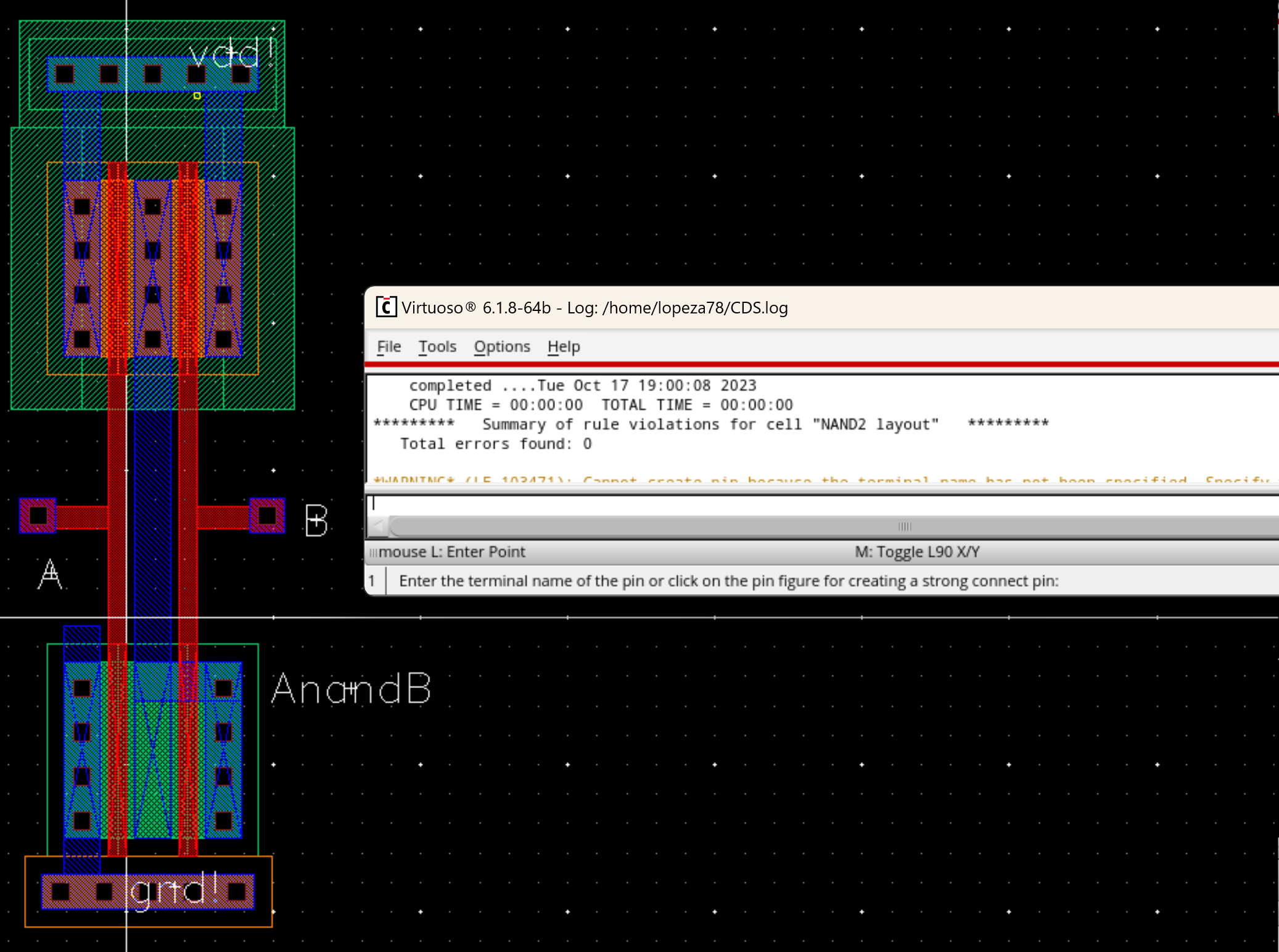
the tutorial we will now develop the proper layout. The follwoing is my layout with its DRC.

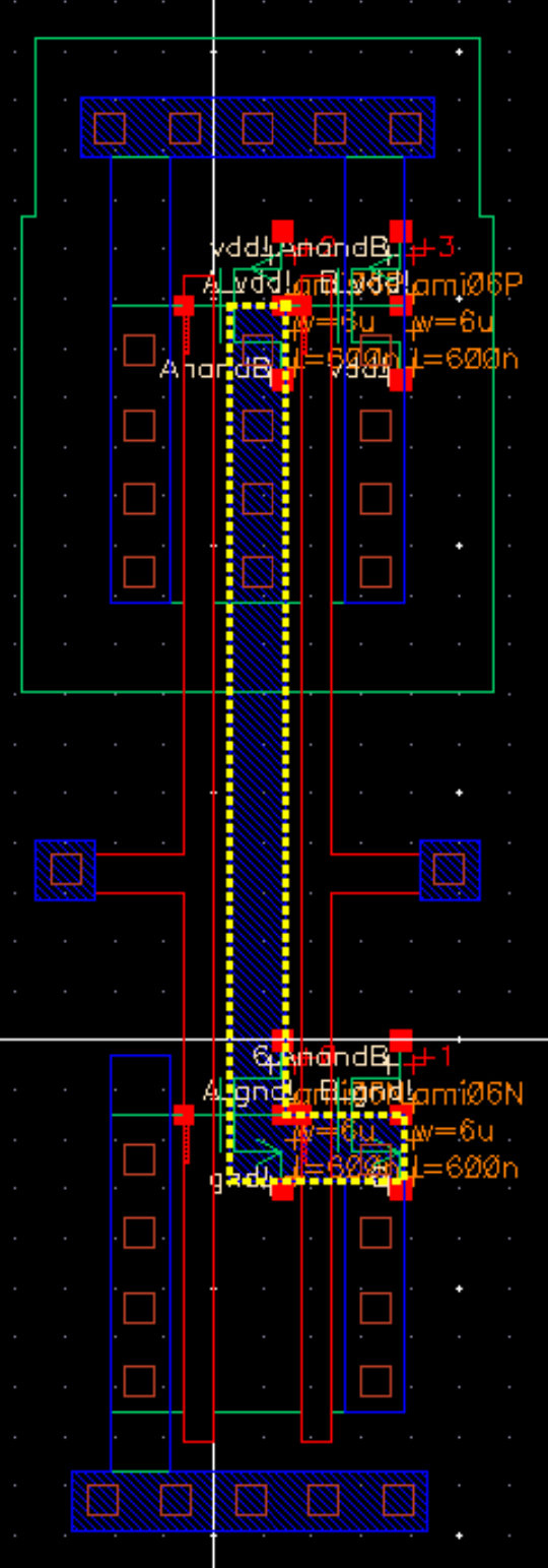
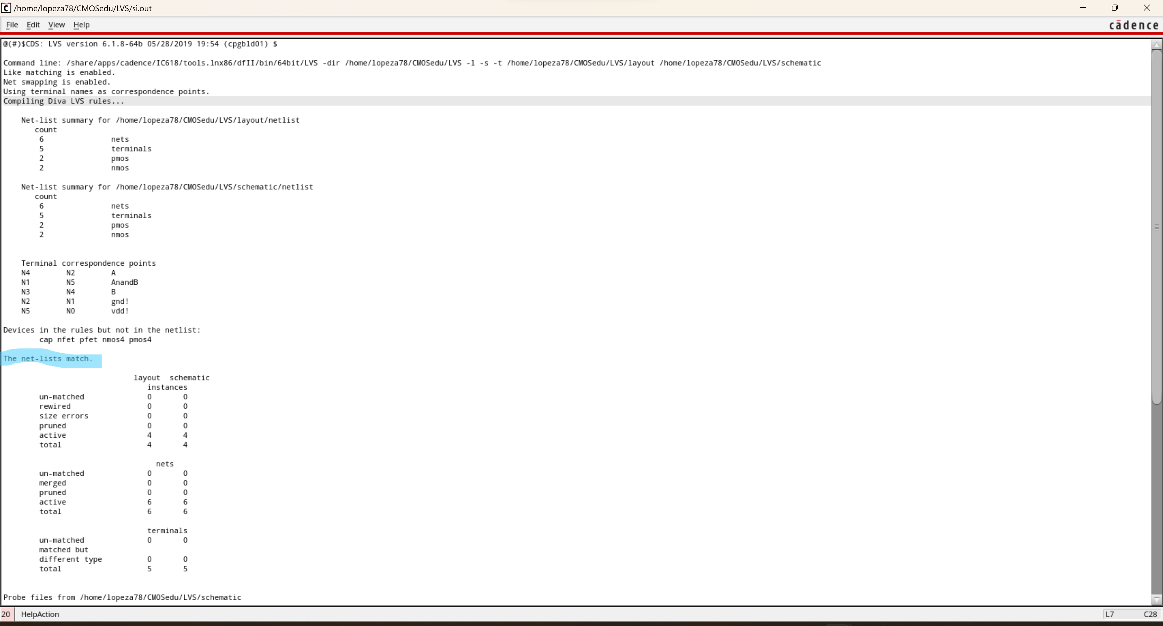
- Now
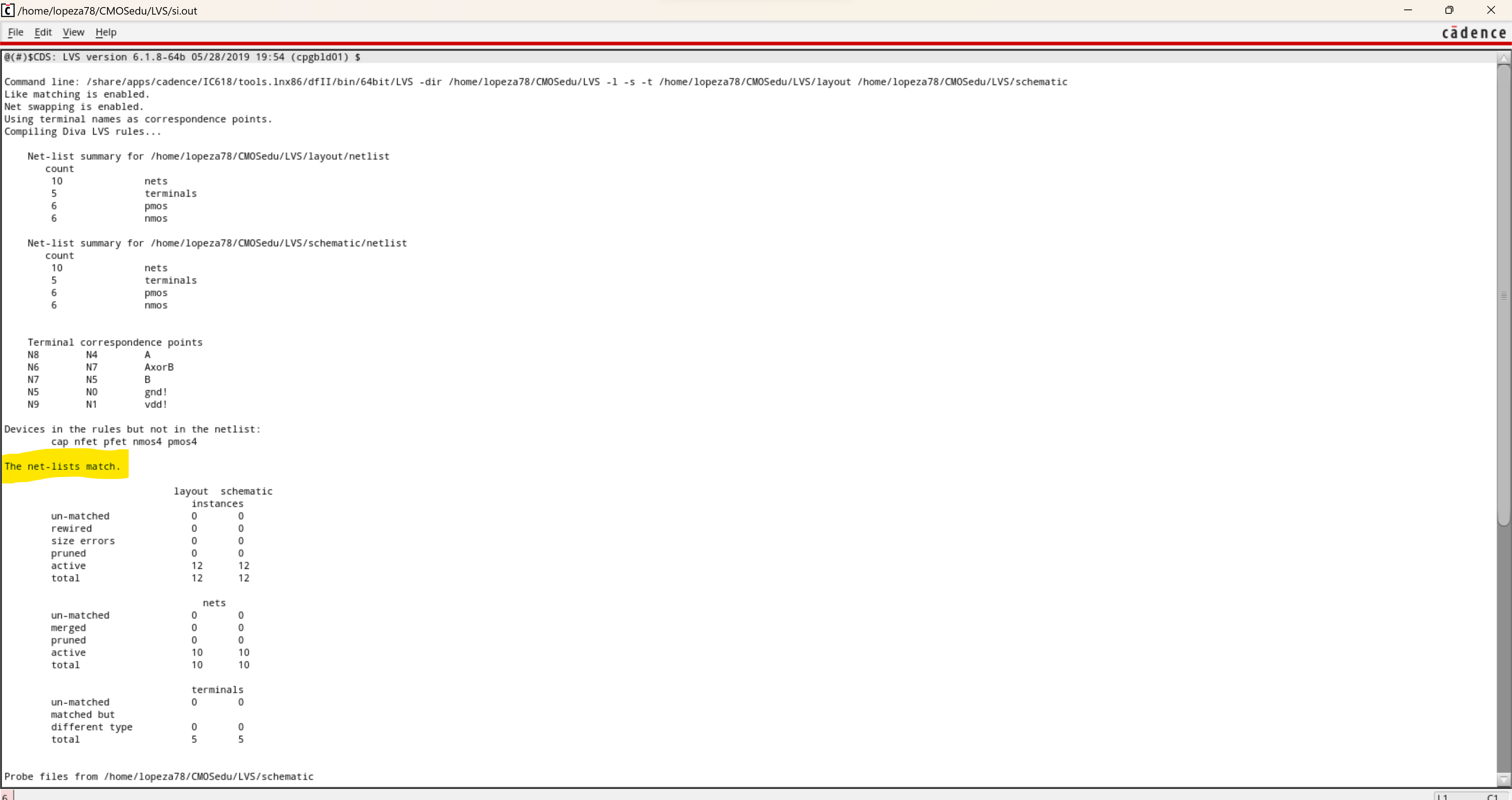
the following is the LVS compared to the schematic previously shown.
(First image shown is the extracted view then the LVS resutls.)


-This concludes our prelab.
Lab Tasks:
- Draft the schematics of a 2-input NAND gate and a 2-input XOR gate using 6u/0.6u MOSFETs (both NMOS and PMOS)
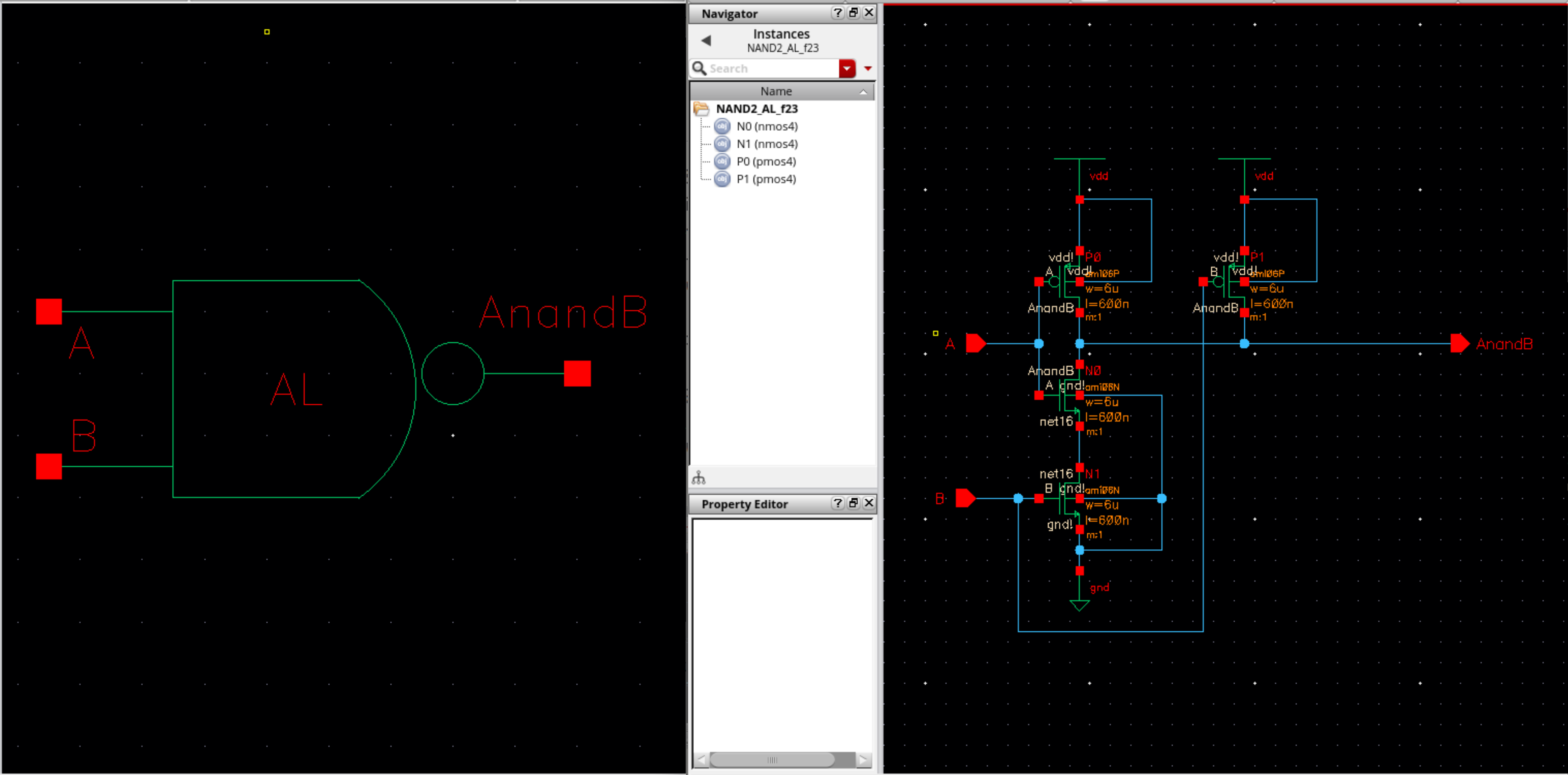
- First I will develop the schematic, symbol and layout for the 2 input NAND gate.
- Here is my schematic and symbol.

- With the schematic and symbol done we now have the layout with its DRC and LVS result.


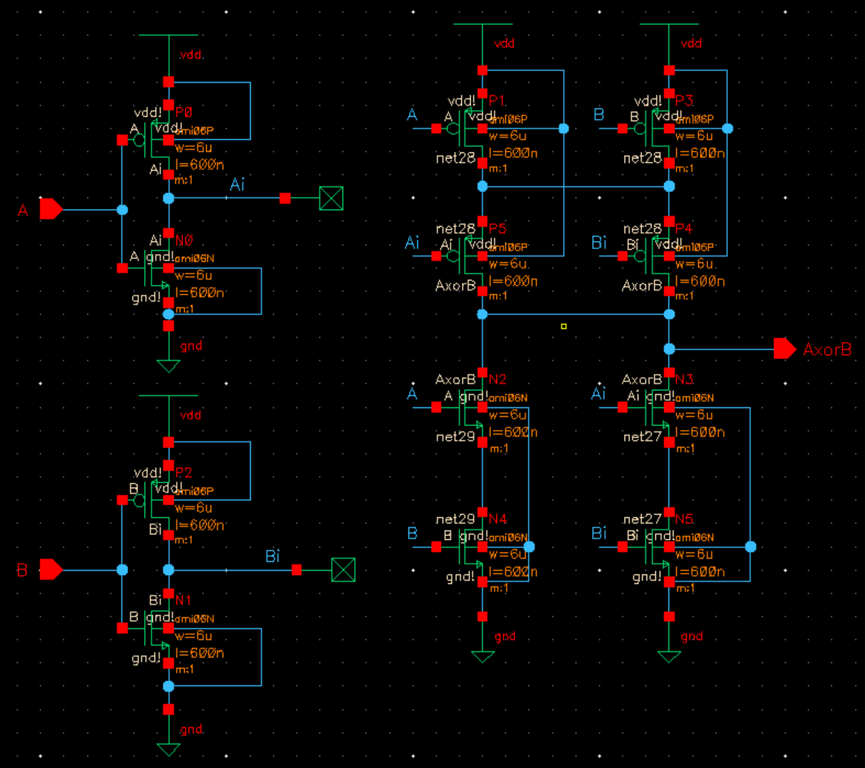
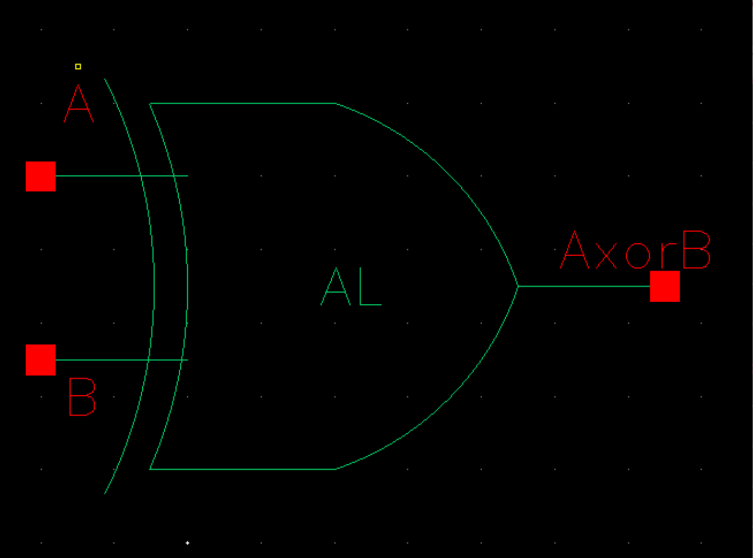
- I will now move on and develop the schematic, symbol and layout for the 2 input XOR gate.
- Here is my schematic and symbol.


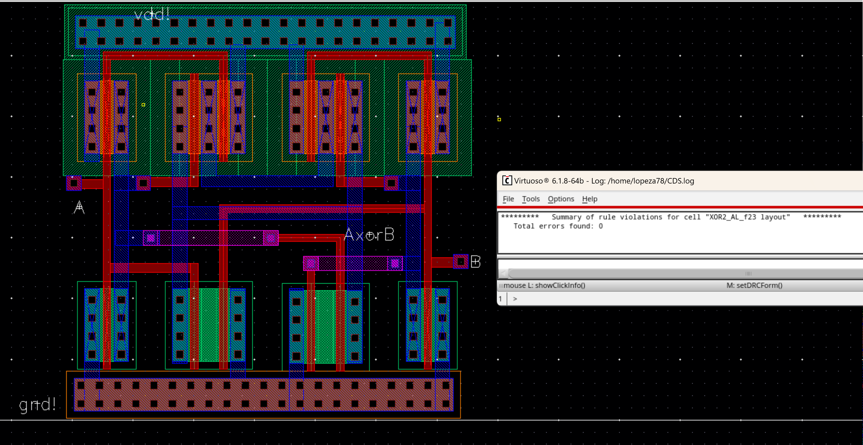
- With the schematic and symbol done we now have the layout with its DRC and LVS result.


- With both
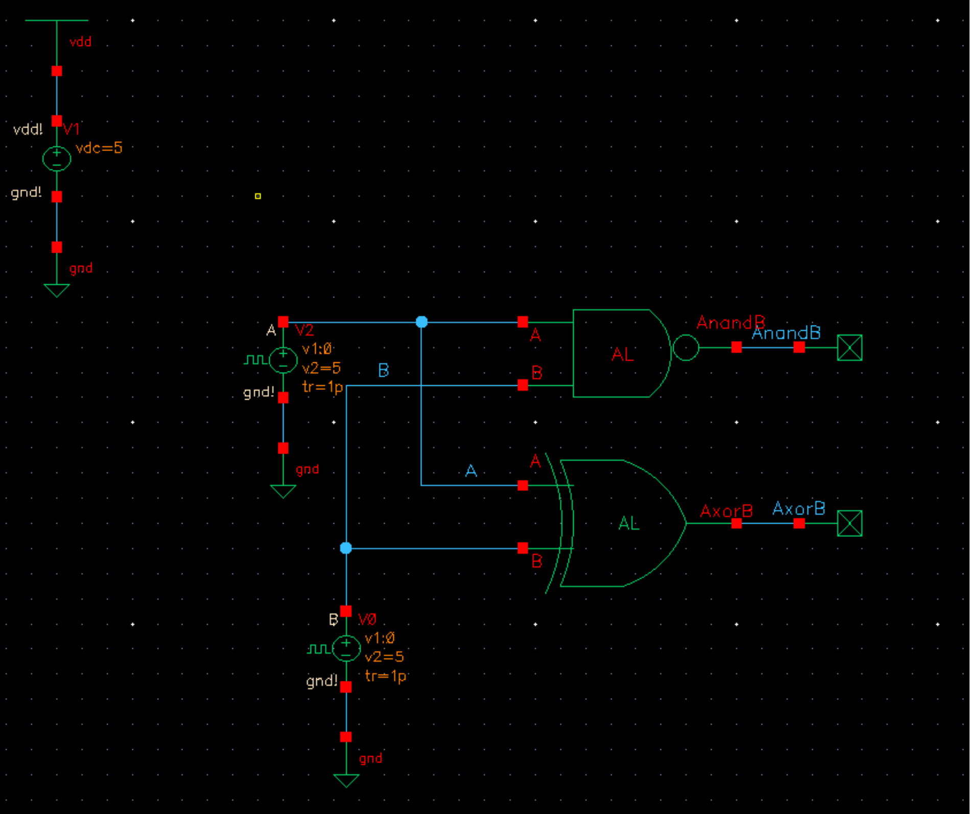
gates created with their respective layouts we will now simulate both.
The following image shows a schematic in which we have two pulse
voltage sources which will act as our input signals. The will
demonstrate all four possible inputs of 00, 01, 10, and 11.

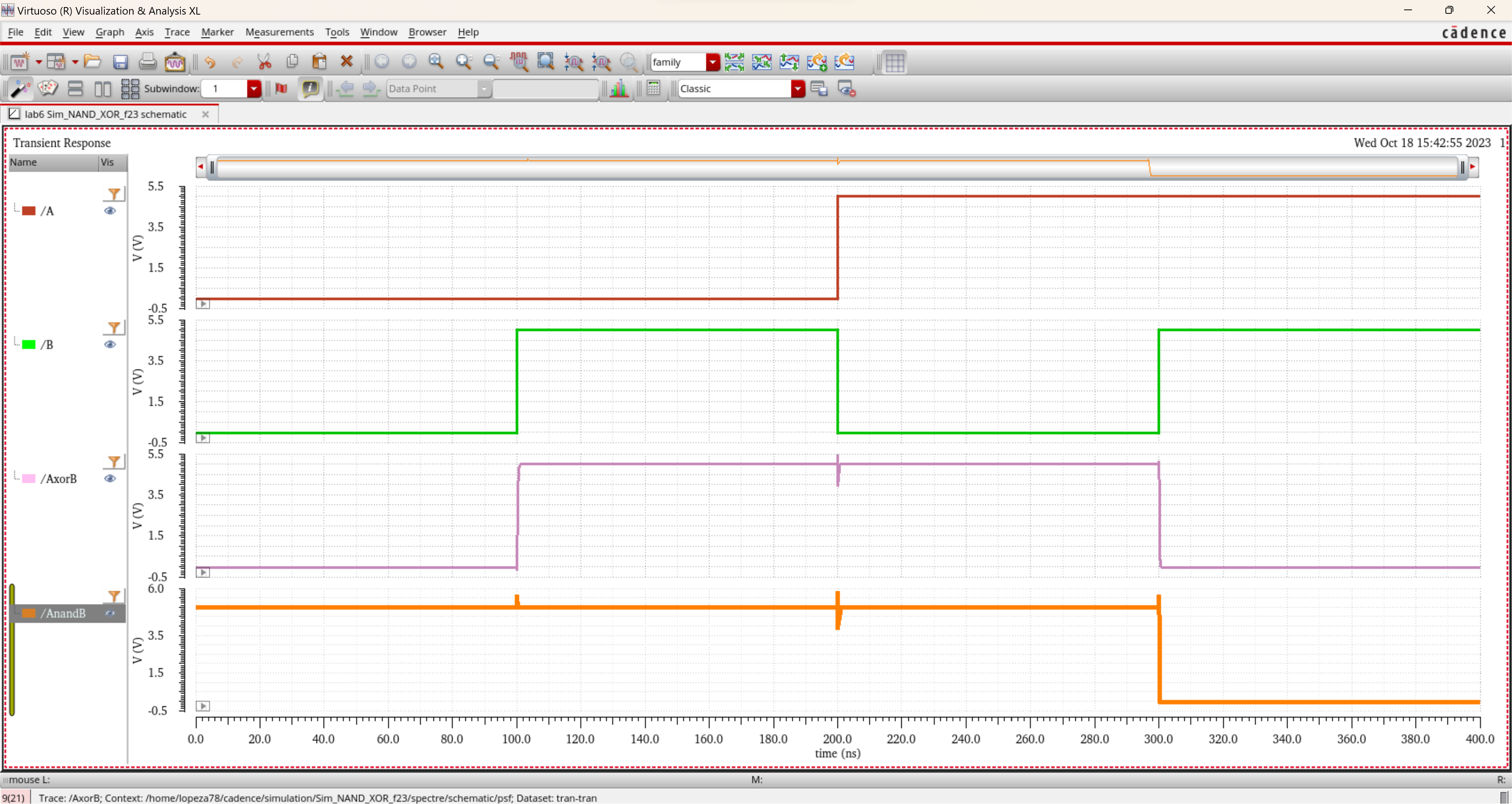
- The following is the plotted inputs and outputs.

- As
you can see from the plotted outputs you see how each rise or fall in
either input causes a small clitch in the output. This can just come
from the changing values of the inputs as they rise or fall from 0 to 5
or vice versa. The sizes of the clitch can be minized by changing the
rise and fall time in our intput pulses.
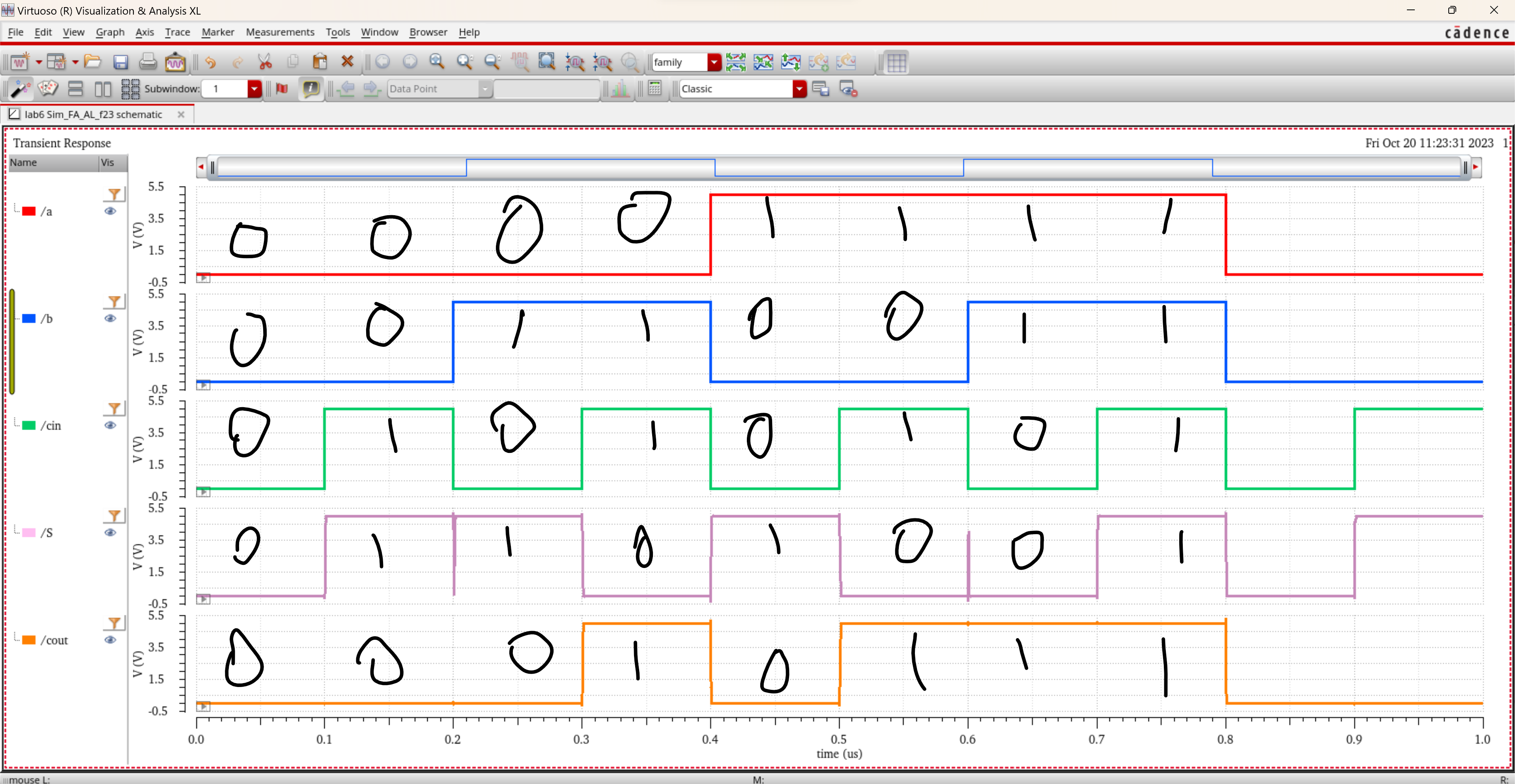
- Using these gates, I will draft the schematic and symbol of a full adder and use the new symbol in a simulation circuit.
- The following is my schematic and symbol respectively.

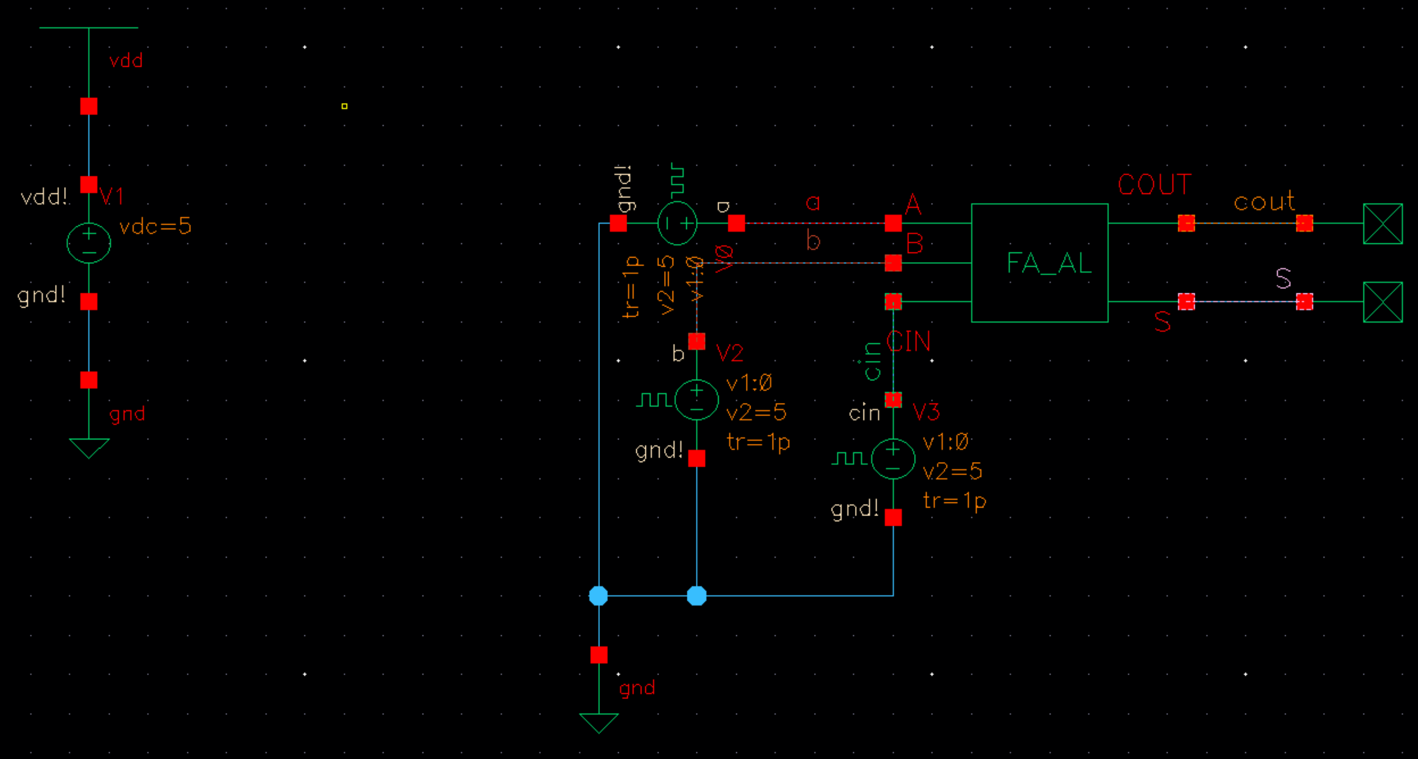
- With
our symbol developed we now use it in the following circuit to simulate
and observe its outputs. First is the circuit then the plotted inputs
and outputs. I labled the plot to show that it accurately represents the truth table.


- Layout the full-adder by placing the 5 gates end-to-end so that vdd! and gnd! are routed
- full-adder inputs and outputs can be on metal2 but not metal3
- DRC and LVS your full adder design
- Here is the final design directory for my lab.
Return
