Lab 5 - EE 421L
Authored
by Anthony Lopez
Email: lopeza78@unlv.nevada.edu
Due Date: October 11, 2023
Lab Description:
- Main objectives
- Develop inverter
- Draft a schematic, layout and symbols of different sized inverters
- Simulate in a designated circuit with varying circuit component values.
Pre-Lab:
- Back-up all of your previous work from the lab and the course.
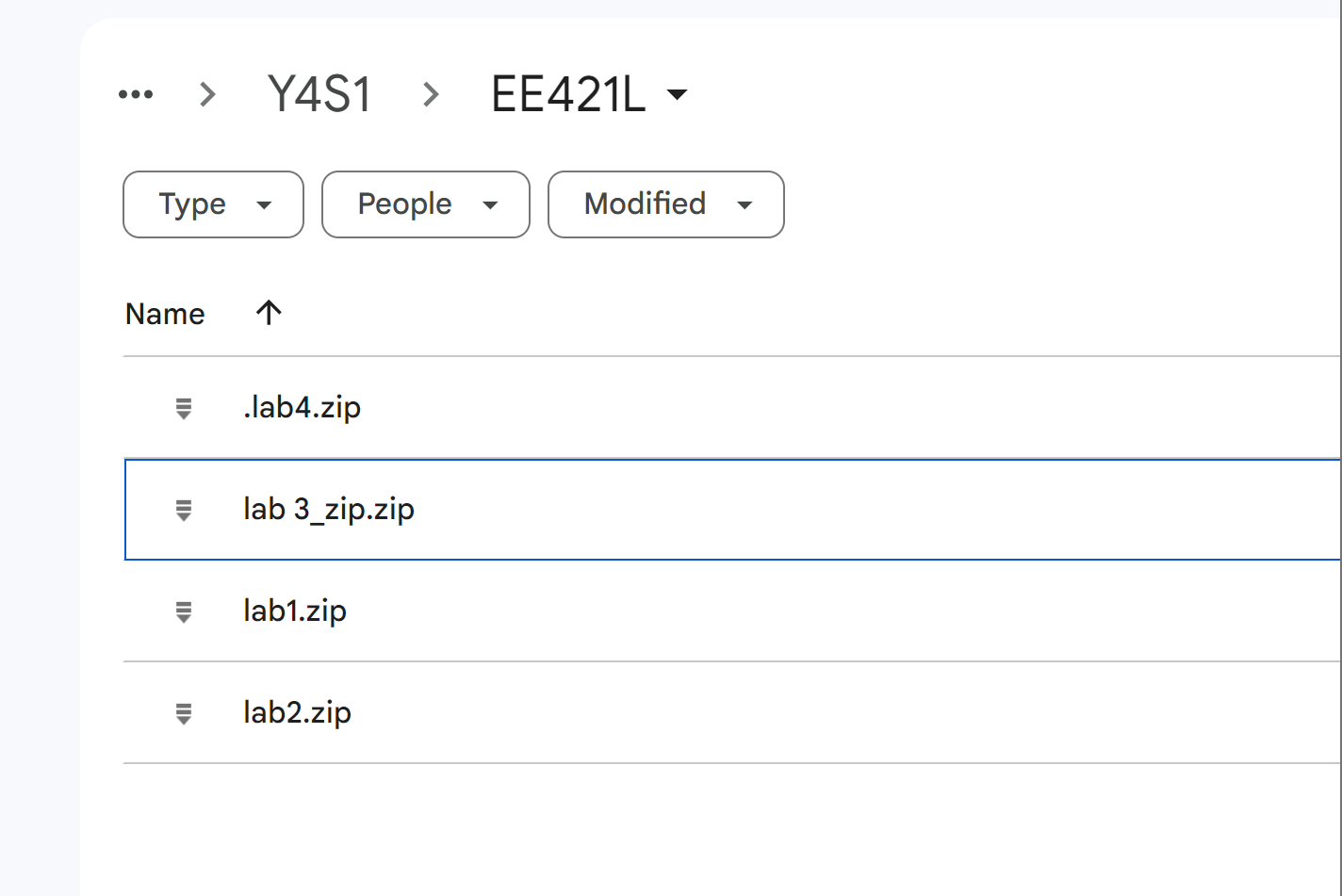
- The following shows my zipped lab 4 file in my drive.
In this third tutorial we’ll draw the schematic, symbol, and layout of a CMOS inverter.
We’ll also simulate the DC behavior of the inverter.
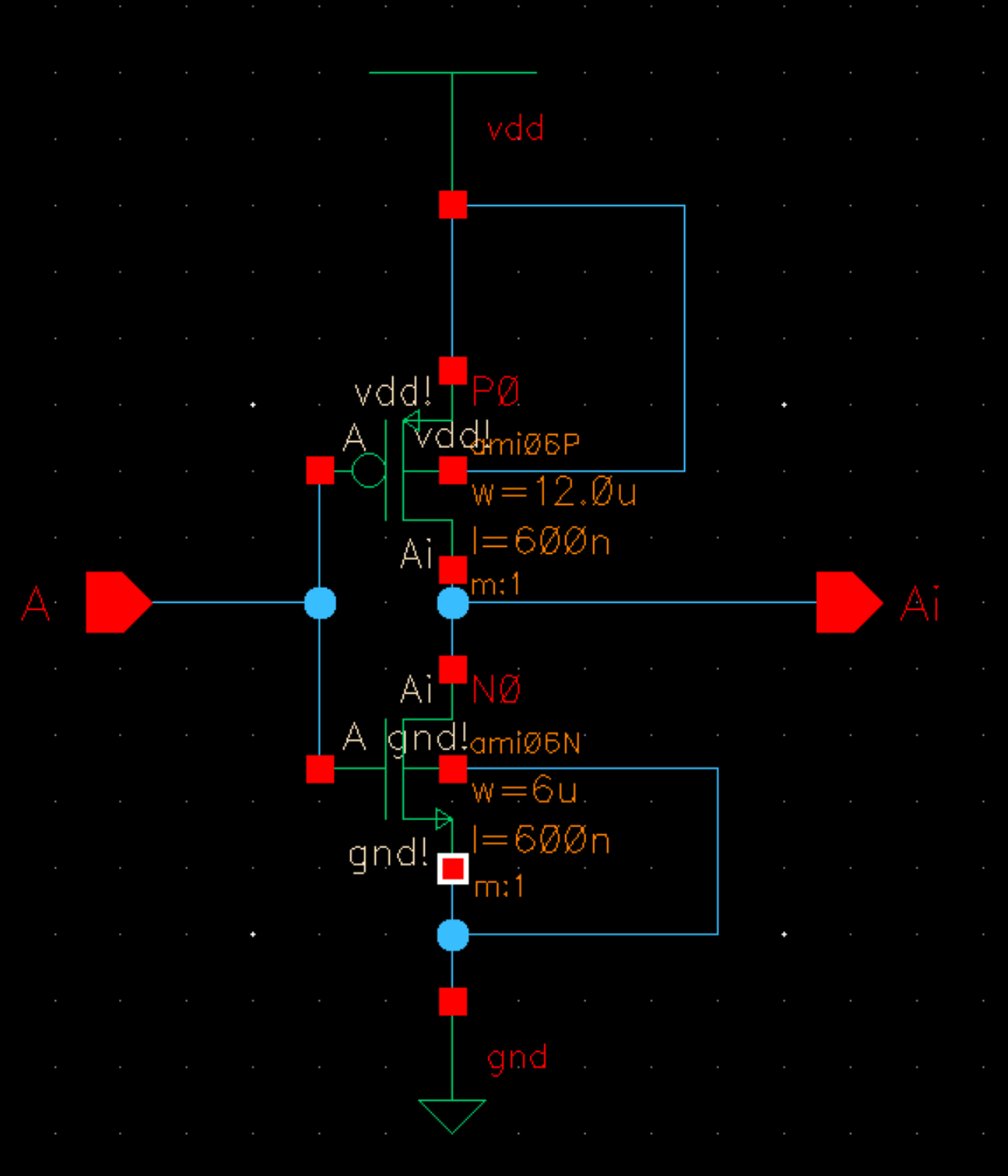
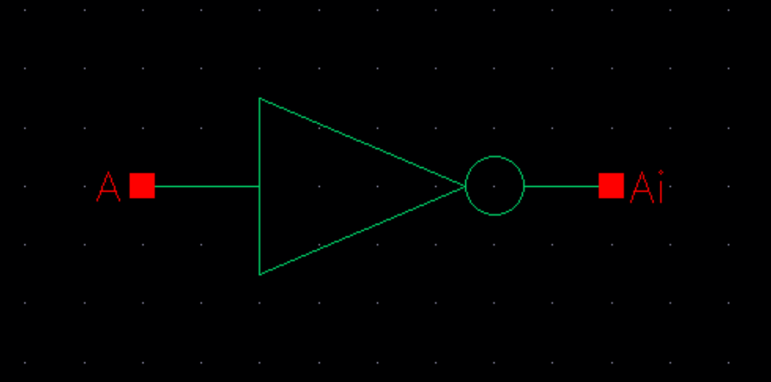
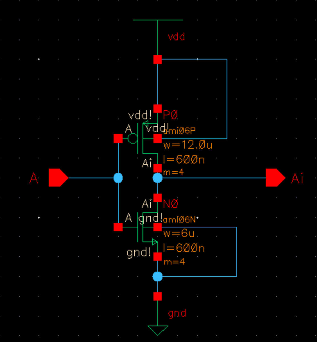
- The following is my developed schematic and symbol for the inverter.
- Continuing
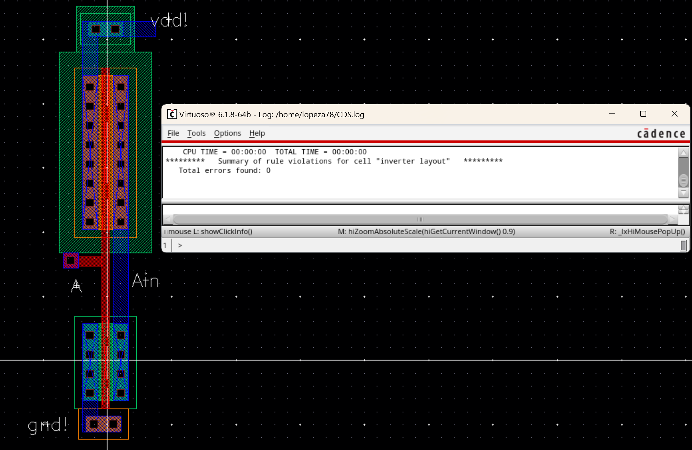
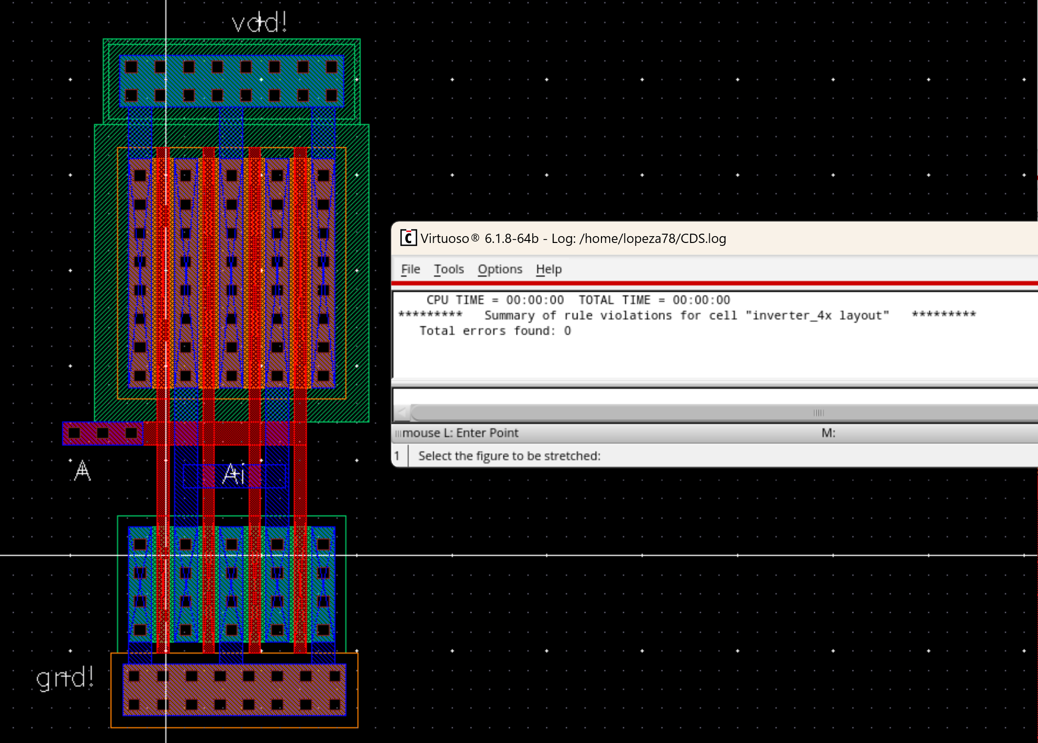
the tutorial we will now develop the proper layout. The follwoing is my layout with its DRC.

- Now
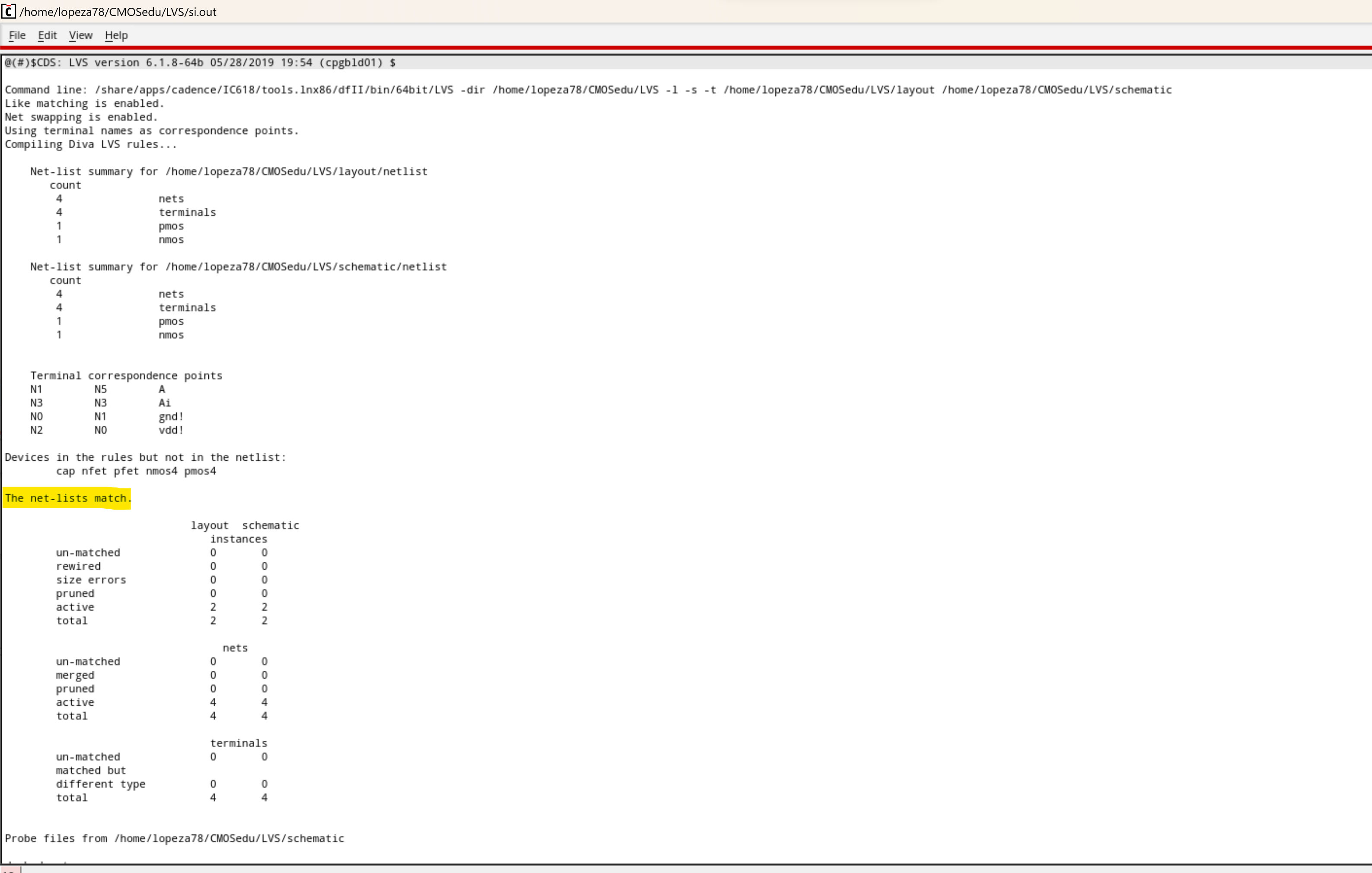
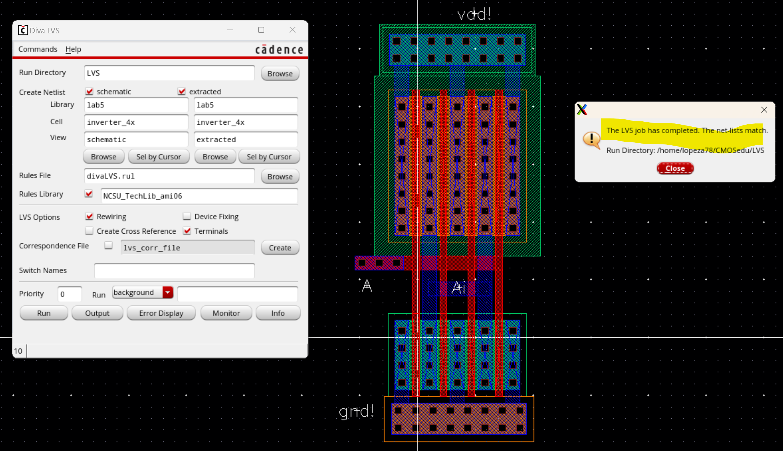
the following is the LVS compared to the schematic previously shown.
(First image shown is the extracted view then the LVS resutls.)


- Finally
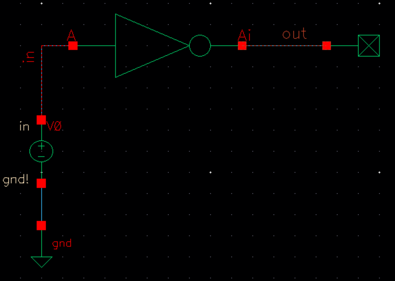
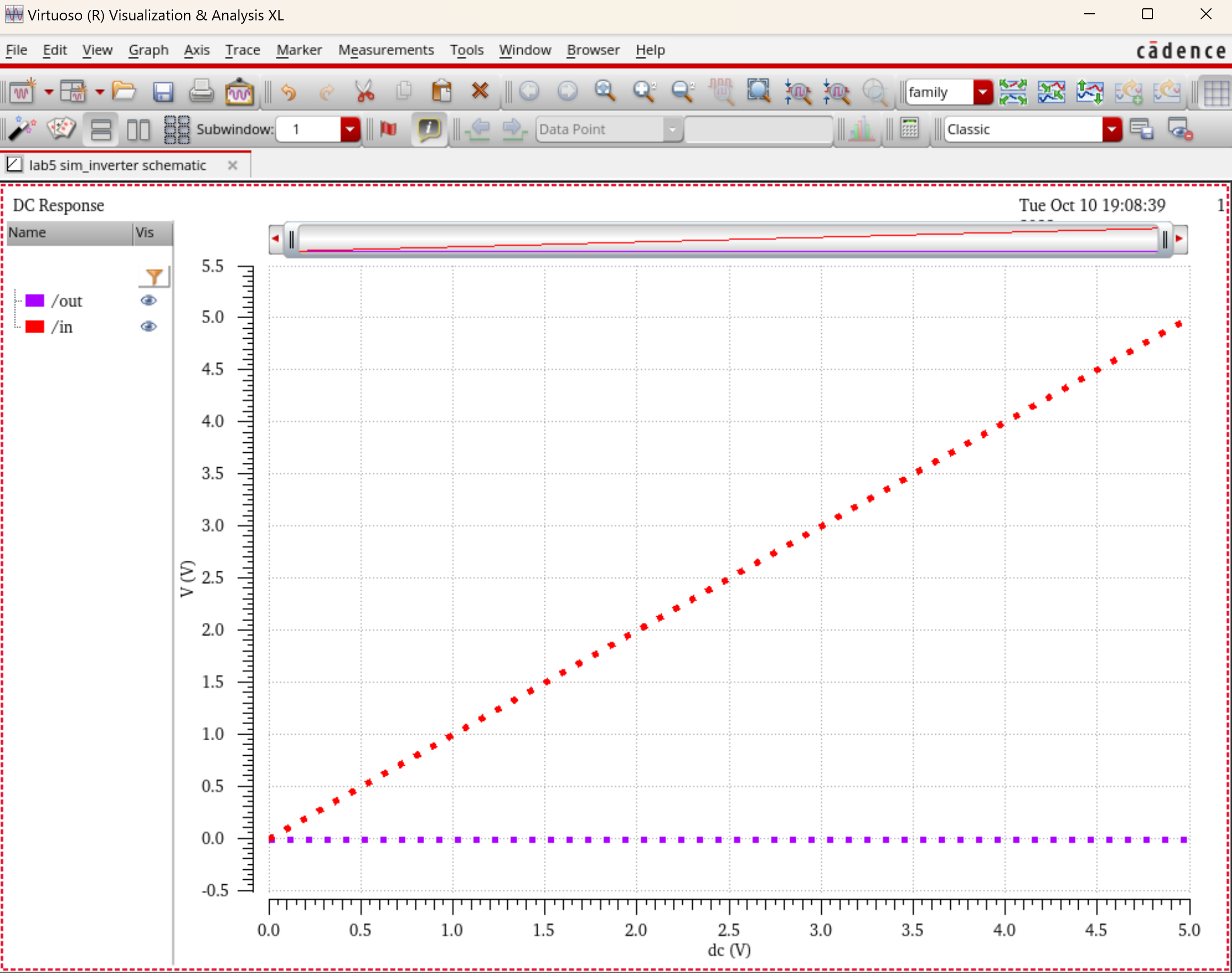
we have our simulations. The first image is the schematic then follows
the results of our dc sweep simulation, having V0 going from 0v to 5v
in increments of 1m.


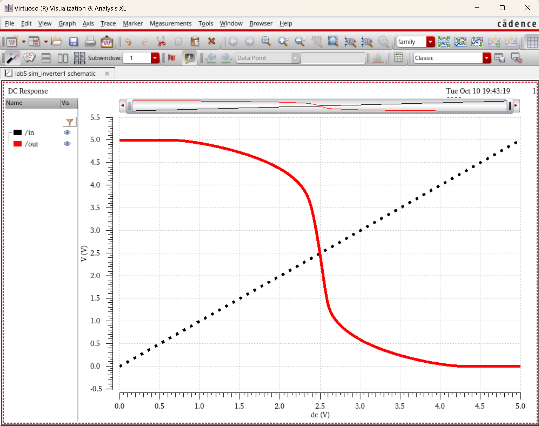
- For
the next simulation we are adding vdd and simulating the same sweep as
the previous, this will give us the appropriate curve for vout since we
are now adding a voltage to vdd. This means we are now appropriately powering/activating our inverter.

- A
quick note is that we can simulate the schematic form the extracted
view. This is just done from setup, then environment, finally just add
extracted.
-This concludes our prelab.
Lab Tasks:
- Draft schematics, layouts, and symbols for two inverters having sizes of:
- 12u/6u (= width of the PMOS / width of the NMOS with both devices having minimum lengths of 0.6u)

- Layout and DRC then LVS results


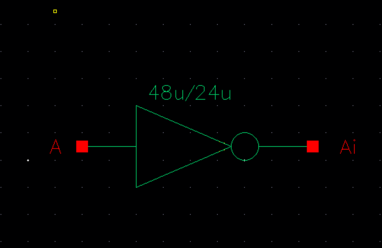
- 48u/24u where the devices use a multiplier, M = 4 (set along with the width and length of the MOSFET), as seen below

- Layout and DRC then LVS results


- Using SPICE simulate the operation of both of your inverters showing each driving a 100 fF, 1 pF, 10 pF, and 100 pF capacitive load.
- First
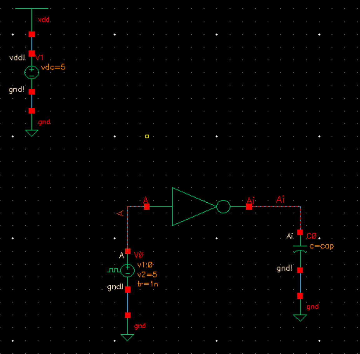
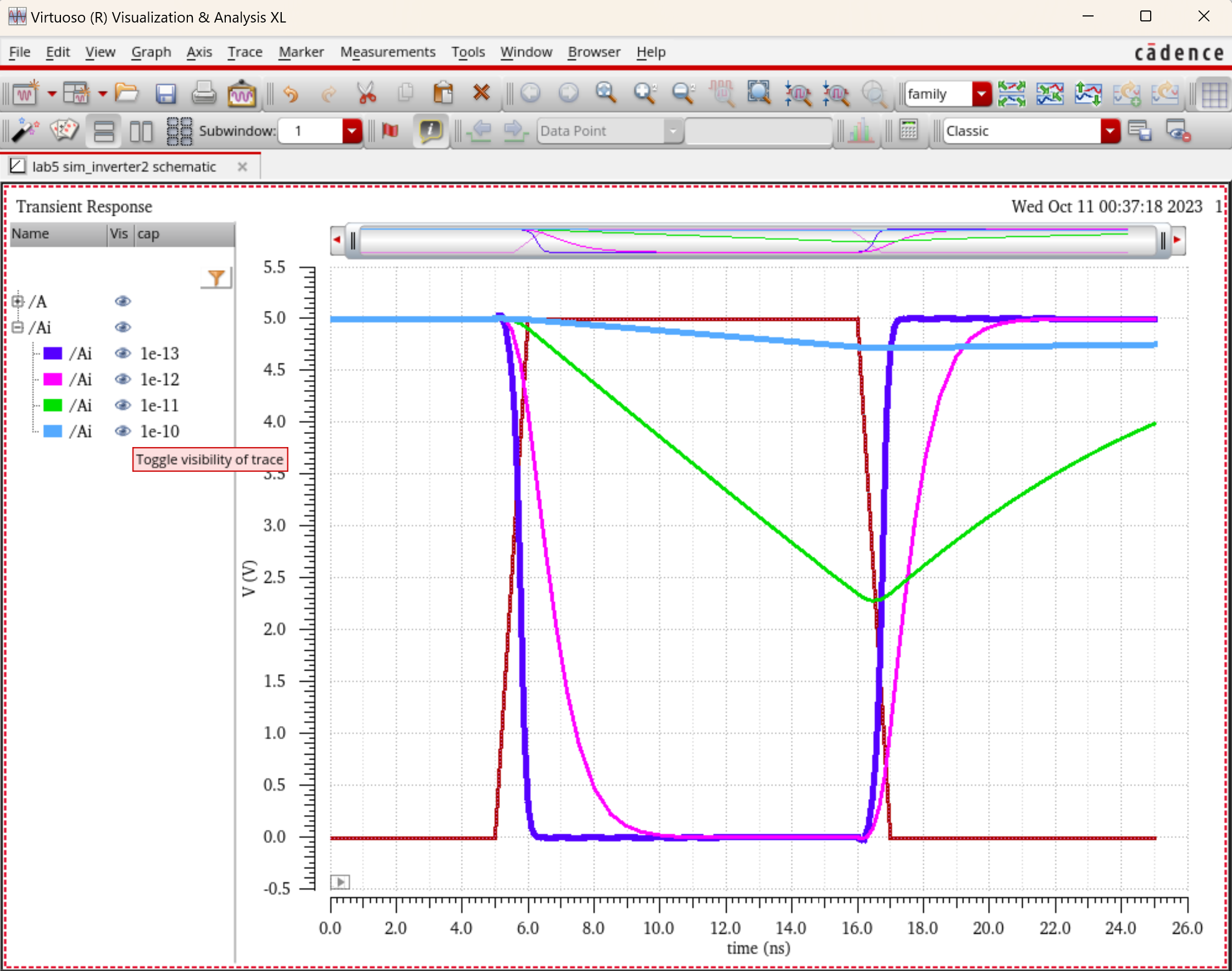
we simulate our 12u/6u inverter. The following images will be my
schematic and simulation resluts respectively. Here I used a parametric
analysis to have the capacitor vary from 100fF to 100pF.


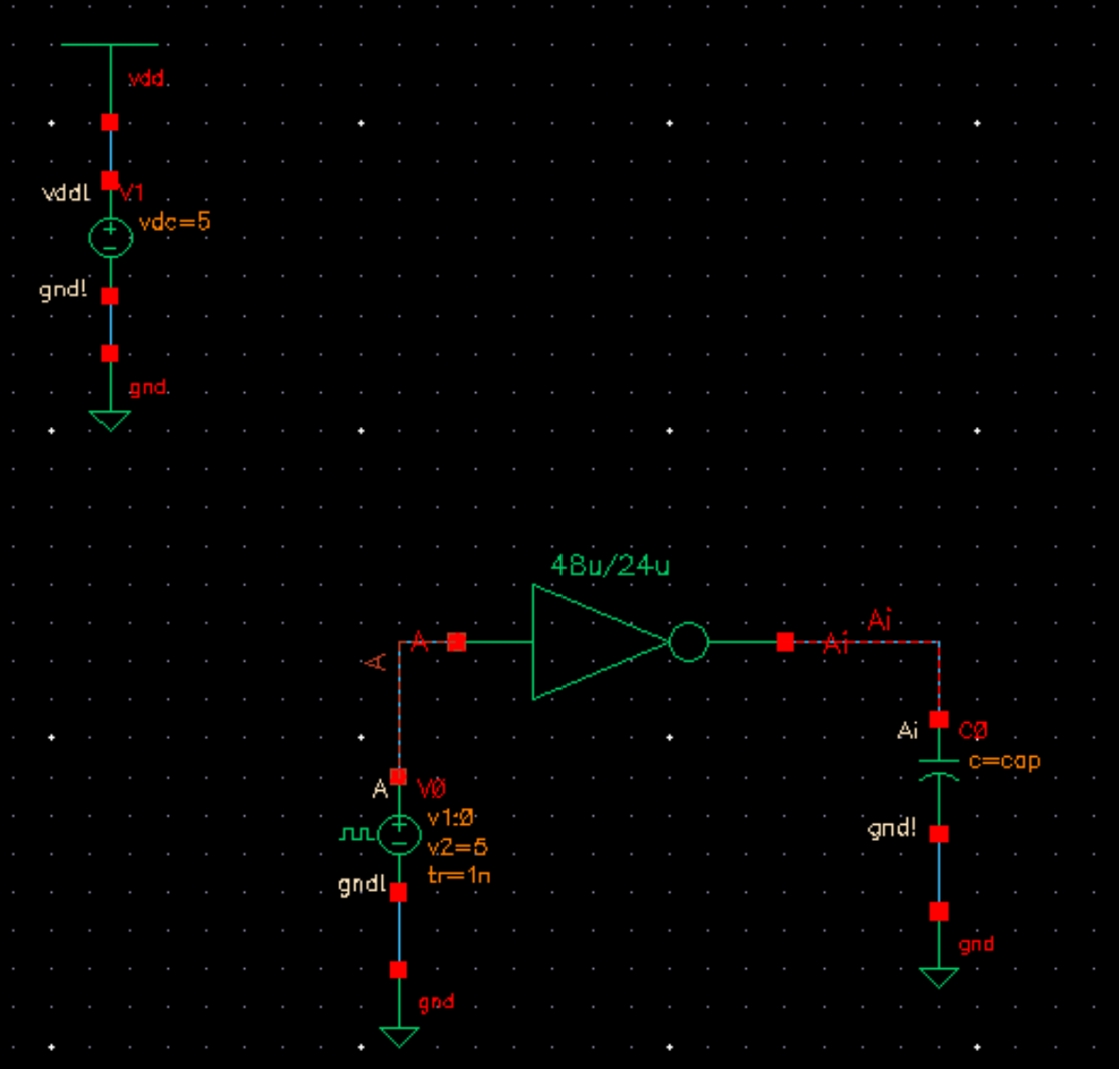
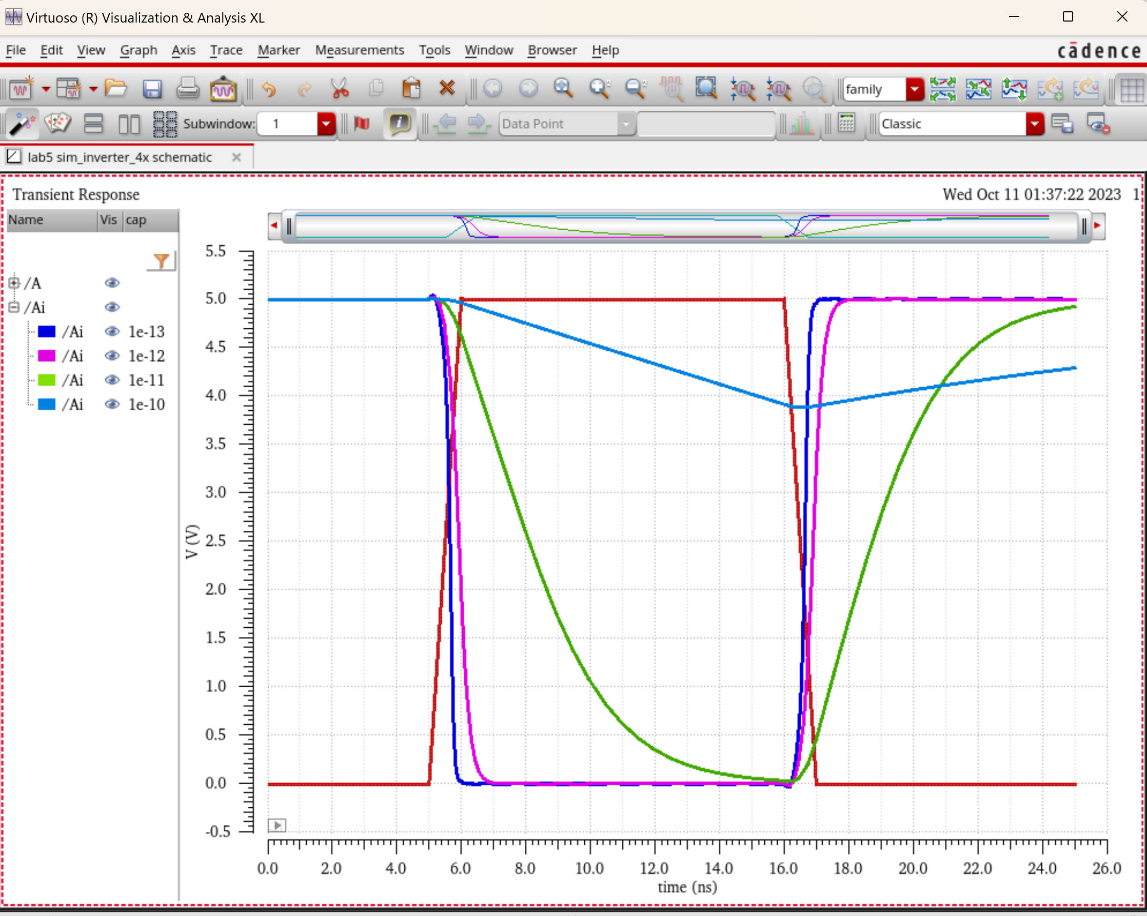
- Now we simulate our 48u/24u inverter. The following images will be my schematic and
simulation resluts respectively. Here I used a parametric analysis to
have the capacitor vary from 100fF to 100pF.


- Lastly
we will look at plots for the same simulation, of our capacitor loads
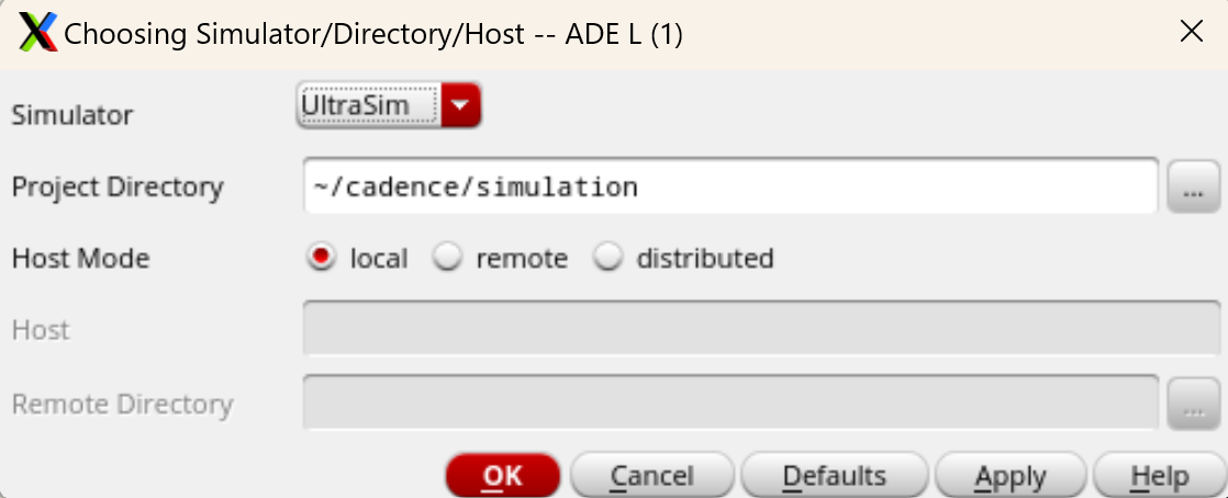
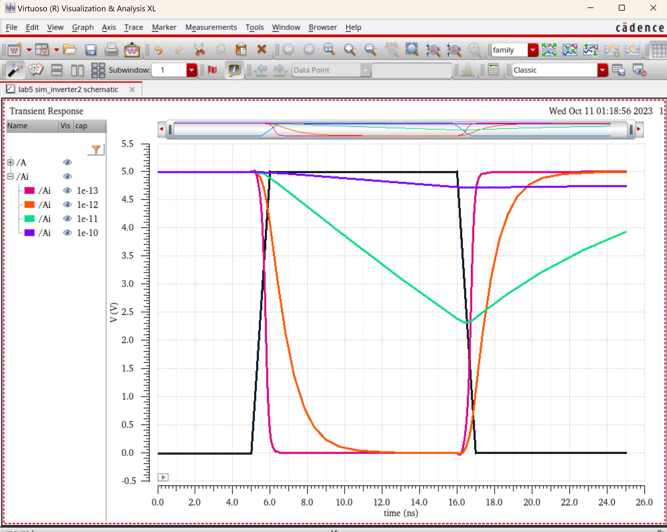
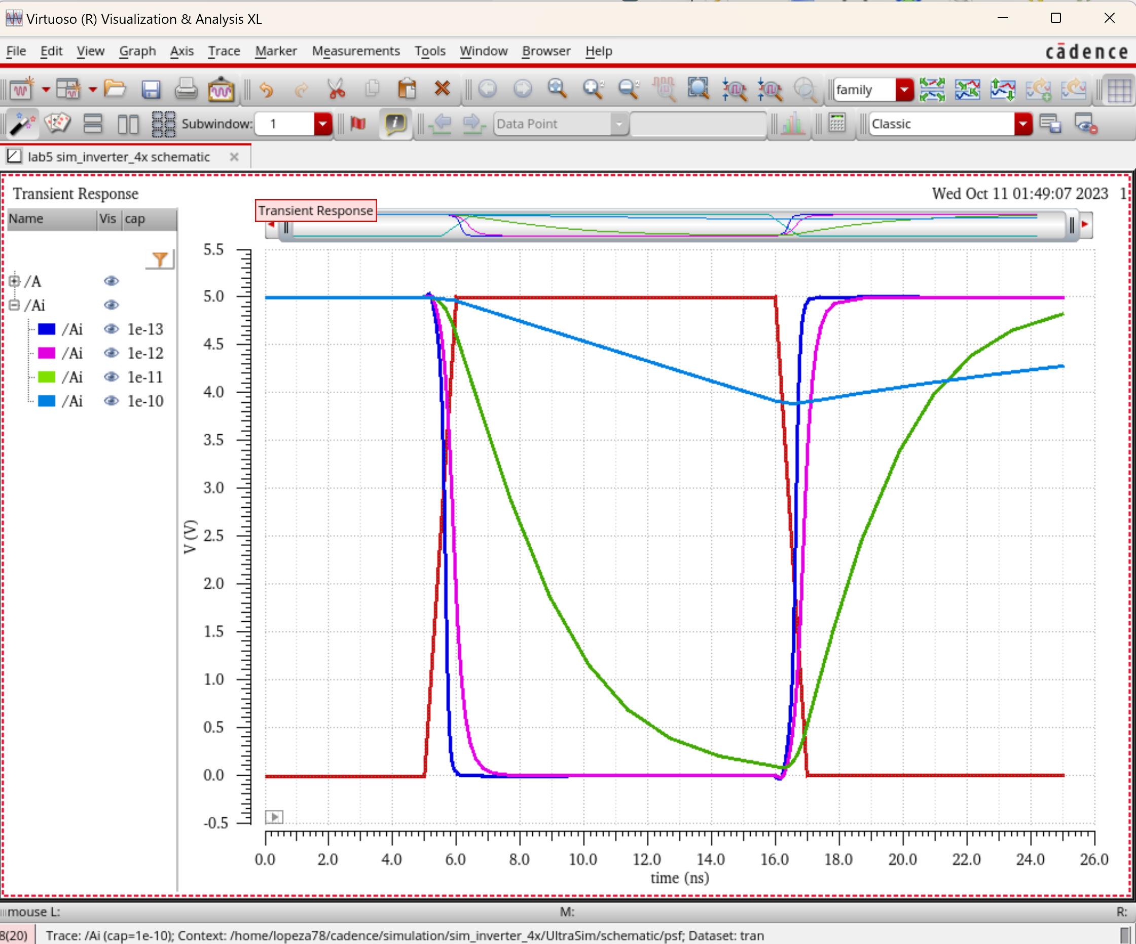
ranging from 100f F to 100pF, however now we will simulate using Ultrasim for our simulator. I again use a parametric analysis to display the varying Ai outputs created from varying capacitance values.

- First is our 12u/6u inverter


-
From both simulators we see that our 48u/24u inverter gives a better
result for Ai. This better performance comes from the additional
fingers , which is why its 48u/24u instead of just 12u/6u. The
additional fingers allow the capacitor to charge and discharge more
effectivly.
- Here is the final design directory for my lab.
Return
