Lab 4 - EE 421L
Authored
by Anthony Lopez
Email: lopeza78@unlv.nevada.edu
Due Date: September 27, 2023
Lab Description:
- Three main objectives:
- Designing an n-well with proper dimentions.
- Using this n-well as a resistor then creating a voltage divider.
- Incorperating
the voltage divieder layout to create a 10 bit DAC. Then verifying our
layout results to our previously made shcematic.
Pre-Lab:
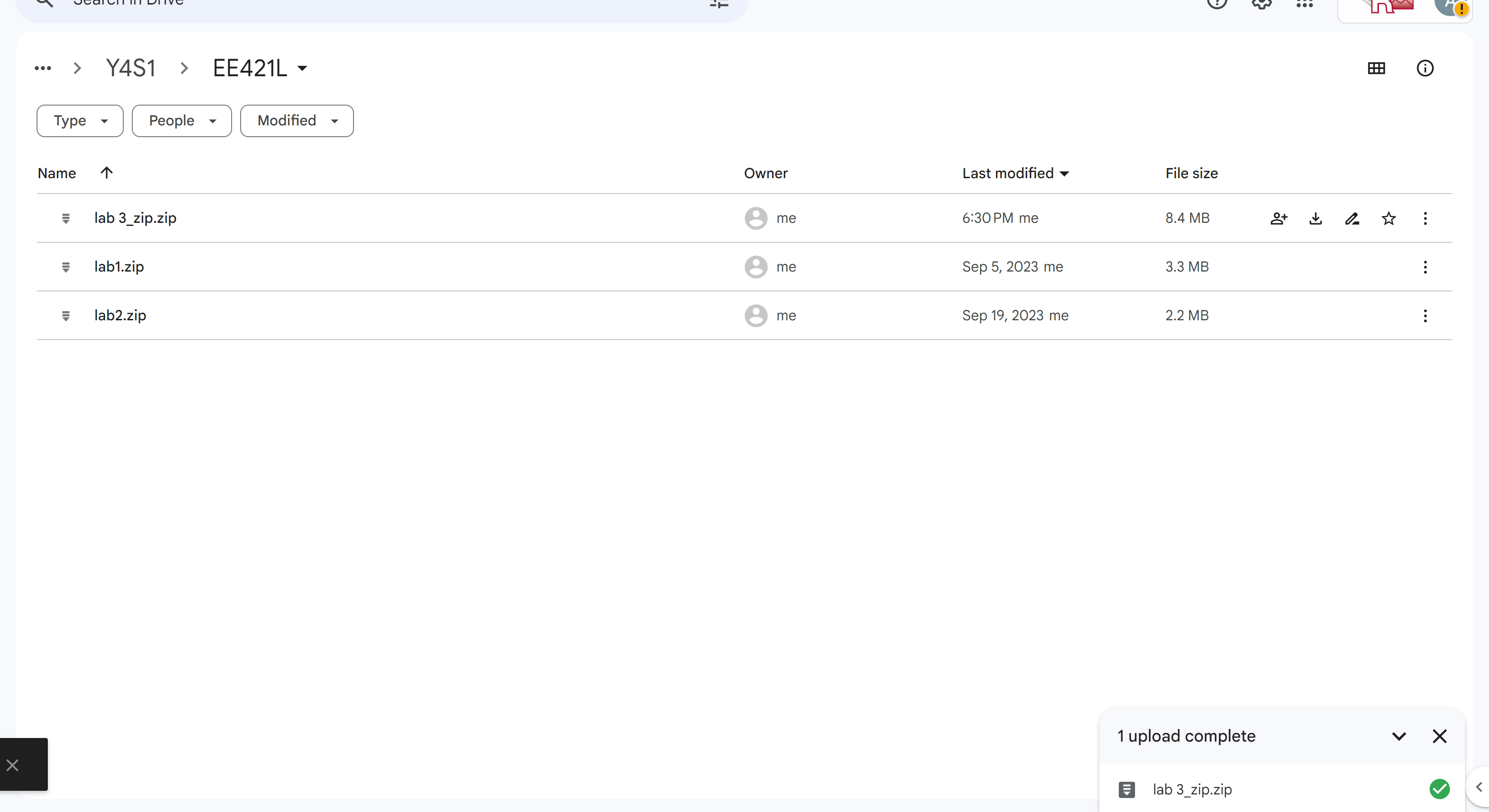
- Back-up all of your previous work from the lab and the course.
- The following shows my zipped lab 3 file in my drive.
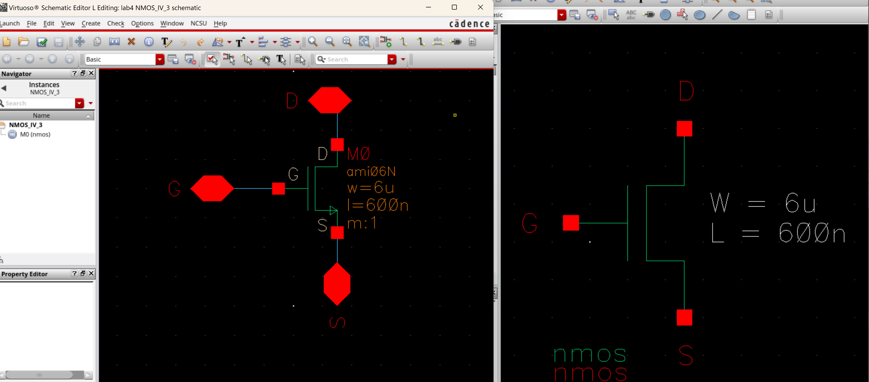
- Go through tutorial 2. For this tutorial we will be developing a transister schematic symbol and layout.
- The following is my developed symbol and schematic for the lecture portion of the class.
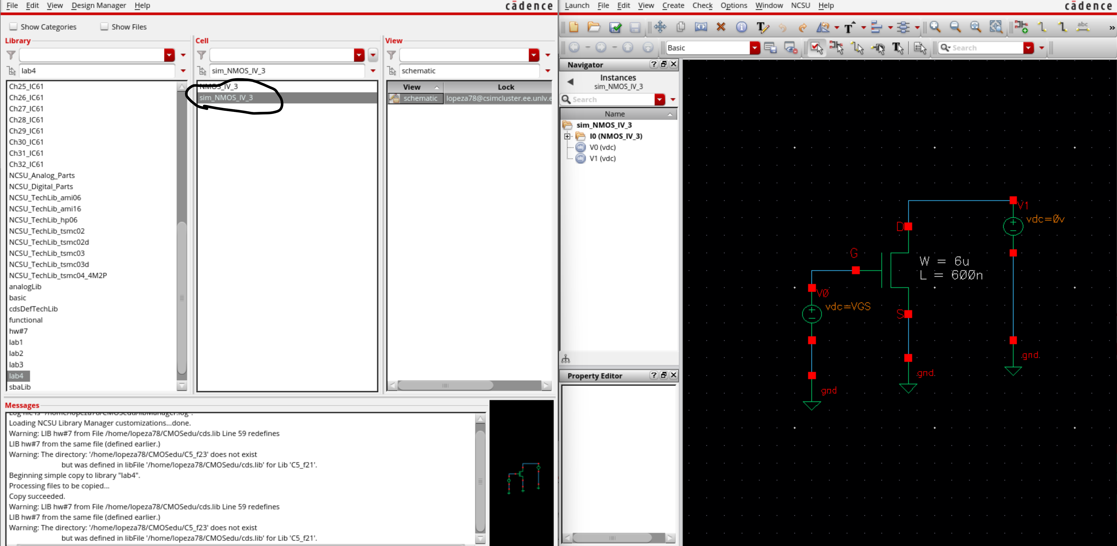
- Continuing
the tutorial we will now use our new symbol in simulation. In our new
cell we will be simulating the following schematic.
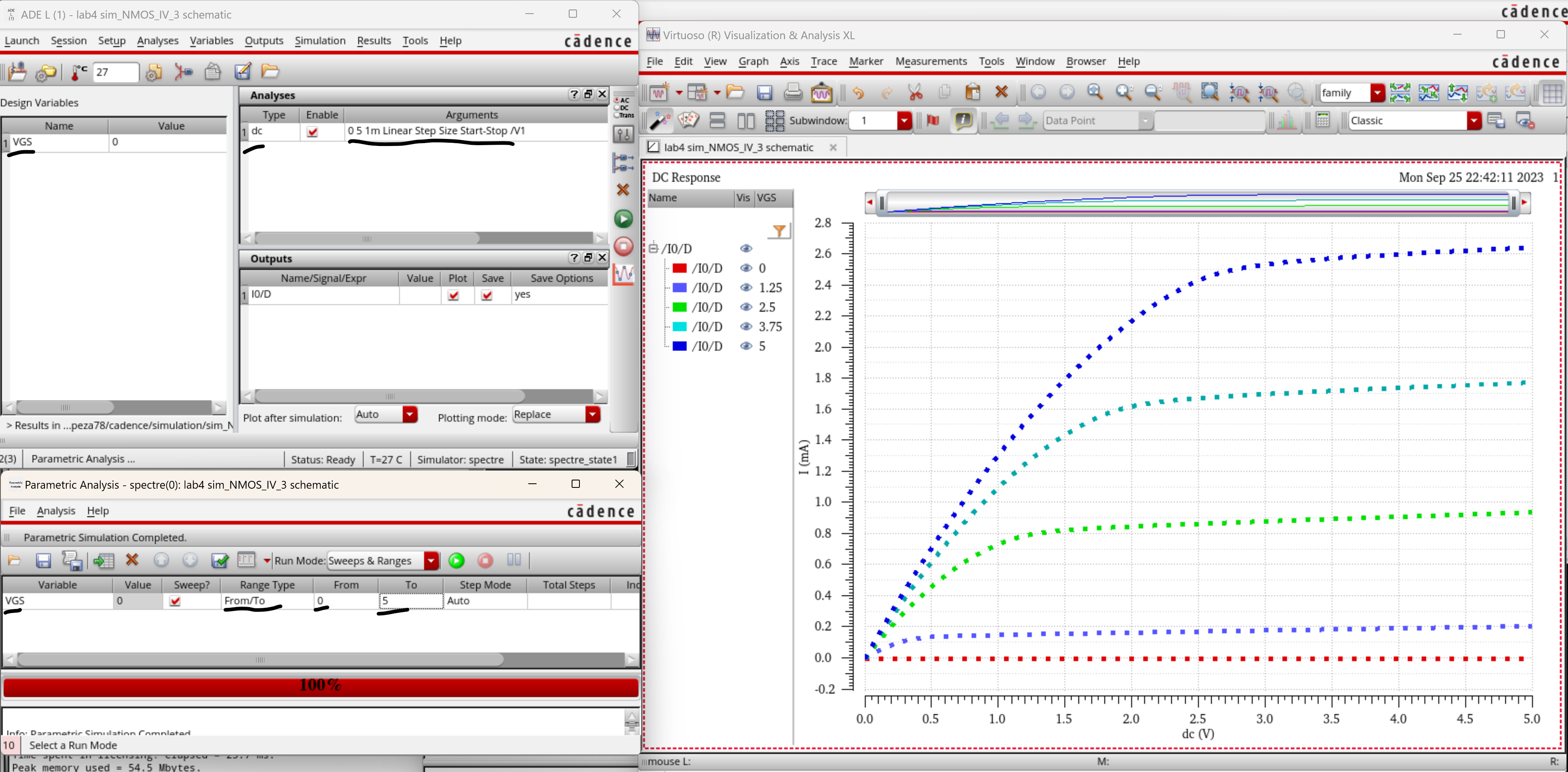
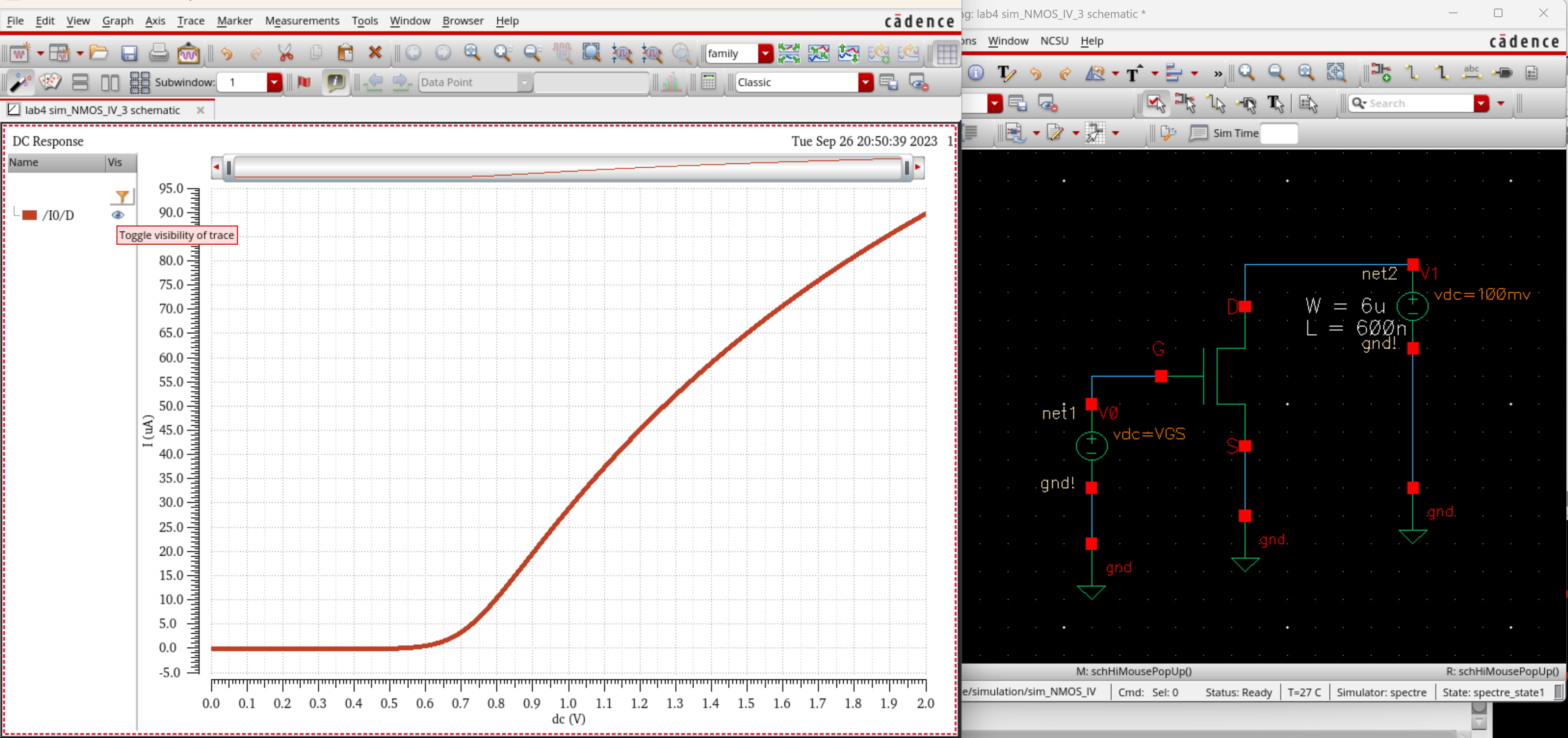
- This
first simulation we will be looking at our net one. We will be doing a
dc sweep on VGS from 0V to 5V. On the left were the associated changes
made to our state and added parametric analysis(which can be found in
tools.)
-
Now that we confirmed our symbol works, we will be designing our
layout for a transistor. We make a layout view for our NMOS_IV_3. After
the view is made we go into our NSCU_TechLib_ami06 library and
instatiate a nmos layout, however we change its dimensions so its 6 um
wide and 600 nm long.
- Now we add the appropriate pins in our metal layers for proper connection.
- However
this form does not pass our LVS thus we switch to a 4 termal transistor
which changes our schematic symbol to the following.The component we use is the nmos4.
- From here we resimulate our schematic in which our symbol is used.

- Seeing that our symbol works fine we go back and change our pins on our layout to then verify our LVS again.
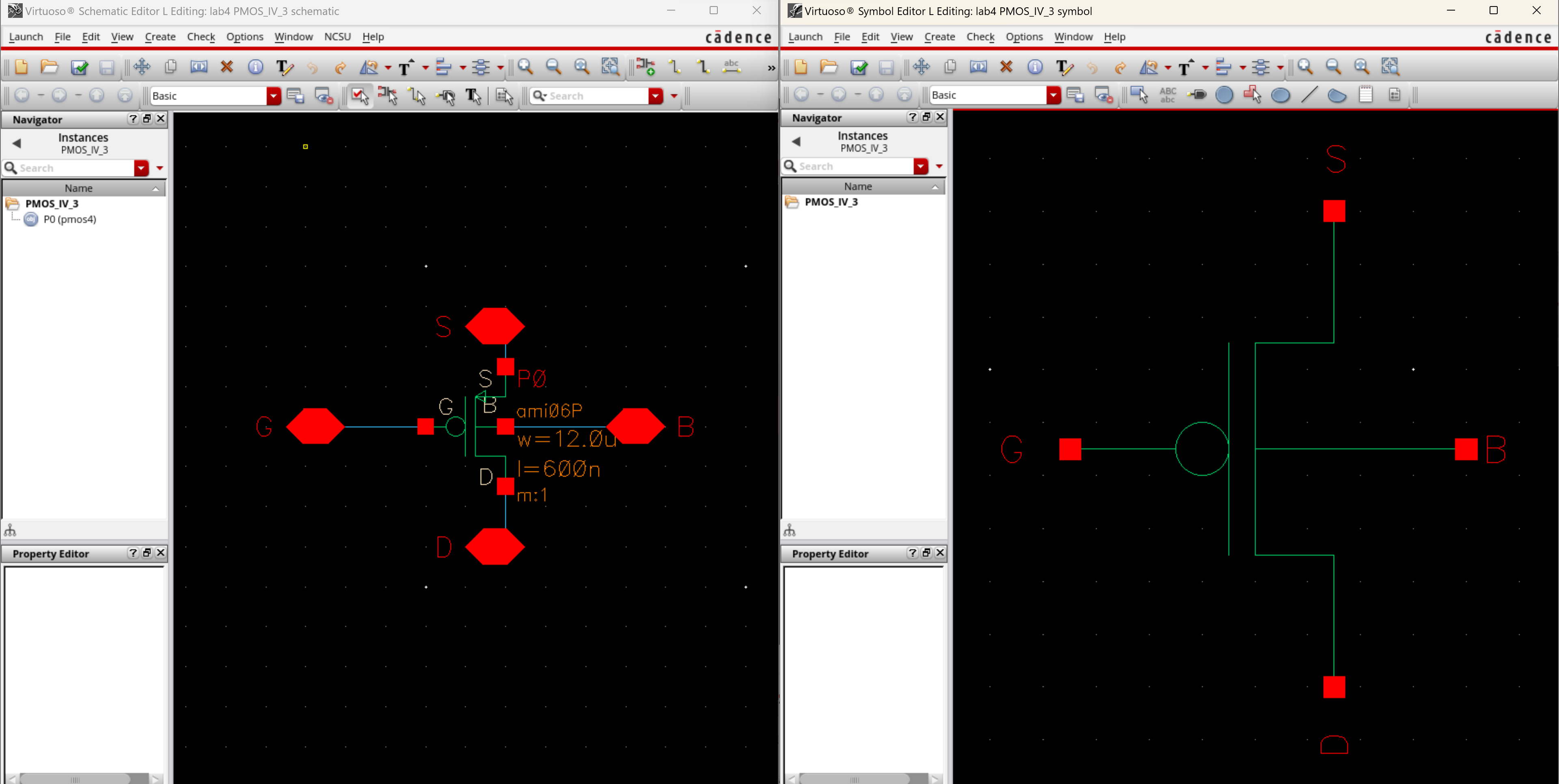
- Now
with our correct nmos layout we will do a pmos layout, schematic and
symbol. However it will be more concise since it is done more
concise in the tutorial. The following is a 4 pin pmos and its
correstponding symbol.
- Next is a layout which will we will DRC extract and conduct an LVS respectivly.
-This concludes our prelab.
Lab Tasks:
- Generate 4 schematics and simulations (see the examples in the Ch6_IC61 library, but note that for the PMOS body should be at vdd! instead of gnd!):
- A schematic for simulating ID
v. VDS of an NMOS device for VGS varying from 0 to 5 V in 1 V steps
while VDS varies from 0 to 5 V in 1 mV steps. Use a 6u/600n
width-to-length ratio.(this was taken from the prelab since our parameters are the same)
- A
schematic for simulating ID v. VGS of an NMOS device for VDS = 100 mV
where VGS varies from 0 to 2 V in 1 mV steps. Again use a 6u/600n
width-to-length ratio.
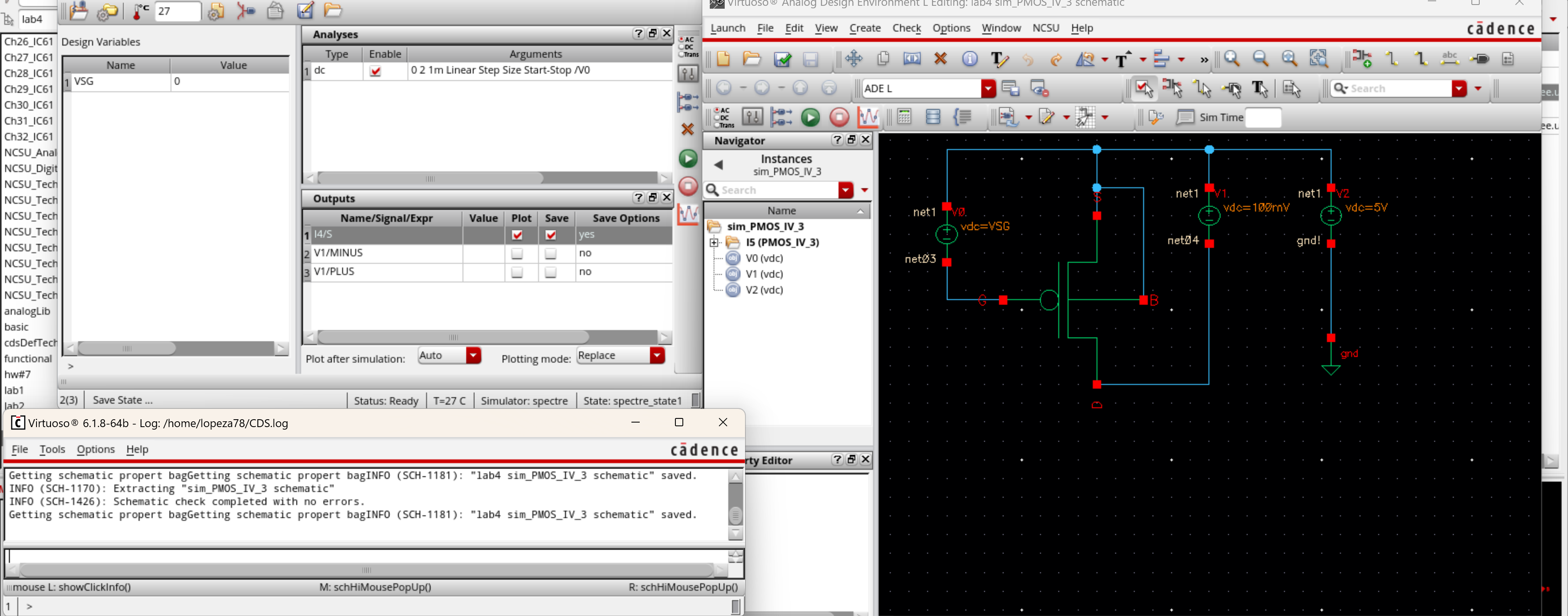
- A
schematic for simulating ID v. VSD (note VSD not VDS) of a PMOS device
for VSG (not VGS) varying from 0 to 5 V in 1 V steps while VSD varies
from 0 to 5 V in 1 mV steps. Use a 12u/600n width-to-length ratio.
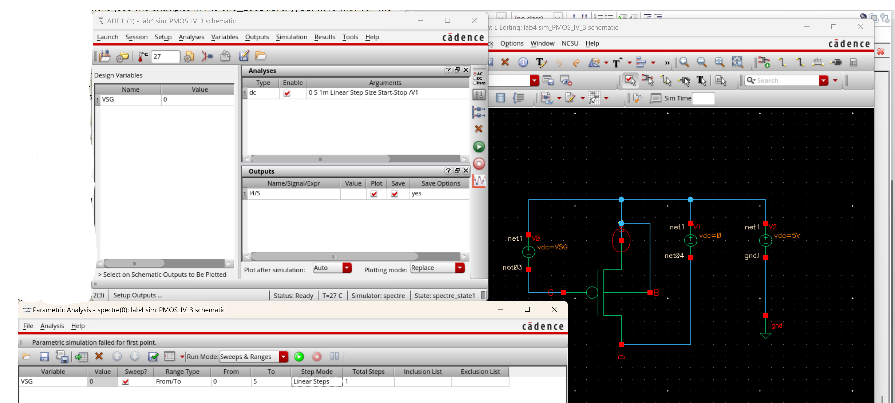
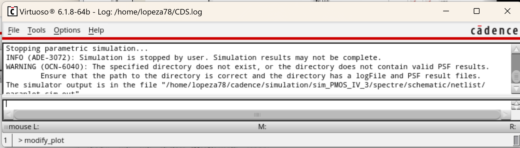
I tried simulating with the following parameters and they kept failing.
The error recieved was on my file directory for output files and said
nothing about how I set up the simulation.
- A
schematic for simulating ID v. VSG of a PMOS device for VSD = 100 mV
where VSG varies from 0 to 2 V in 1 mV steps. Again, use a 12u/600n
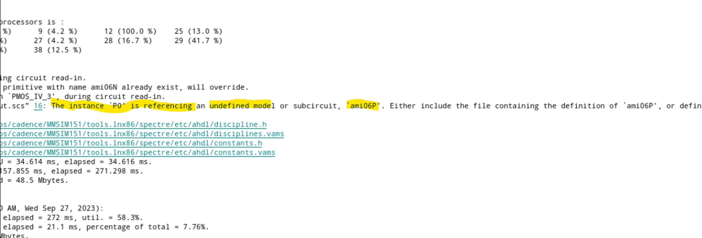
width-to-length ratio. (I see that error is coming from my circuit in
which I developed my symbol. However no error shows up when I save and
check both circuits and this is the same symbol from the prelab which
shows that the LVS is correct as well.)
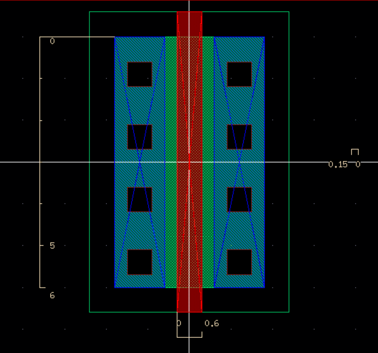
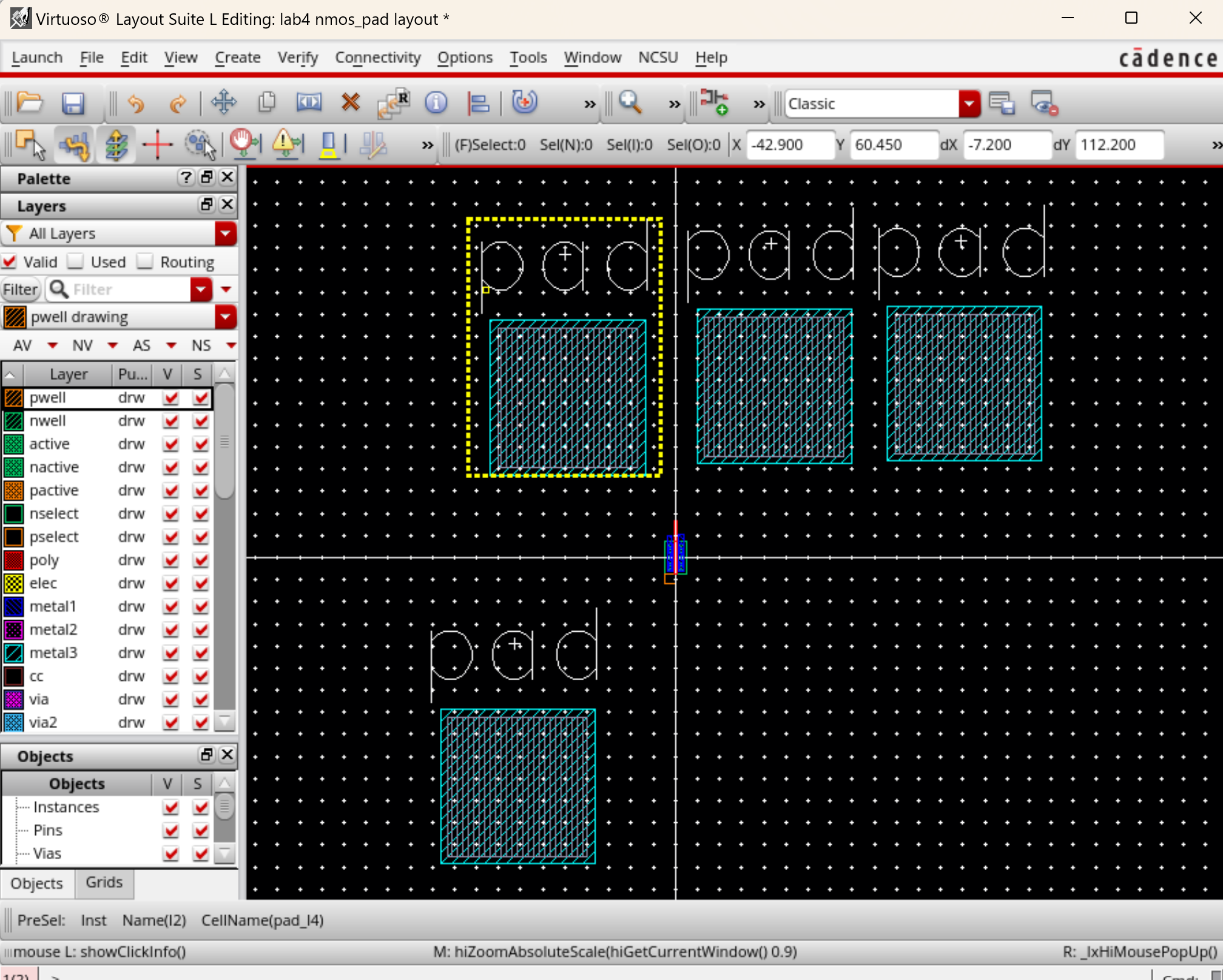
- Lay
out a 6u/0.6u NMOS device and connect all 4 MOSFET terminals to probe
pads (which can be considerably smaller than bond pads [see MOSIS design rules] and directly adjacent to the MOSFET (so the layout is relative small).
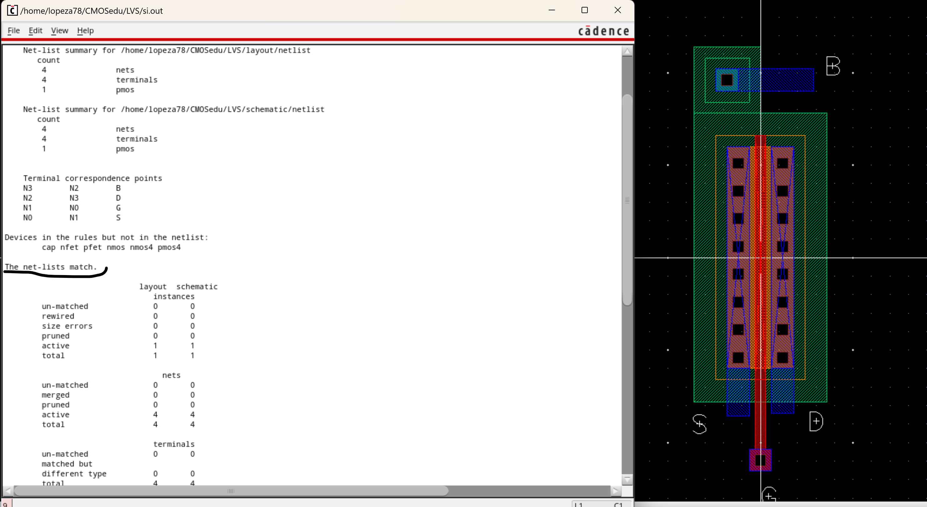
- Show your layout passes DRCs. Just what I have done from layout.
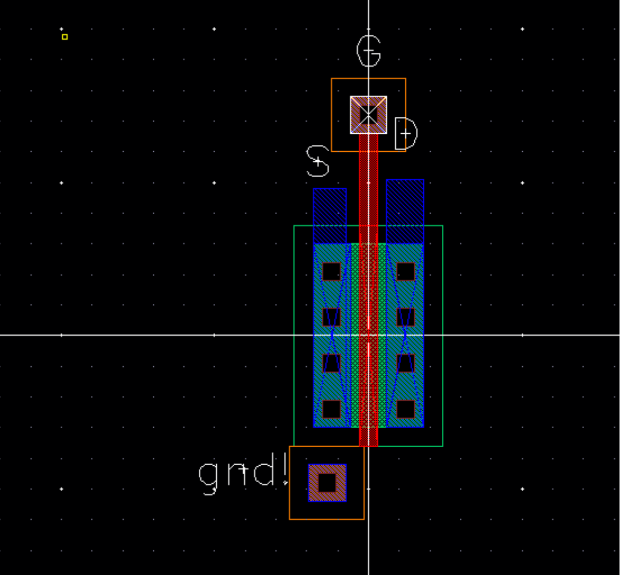
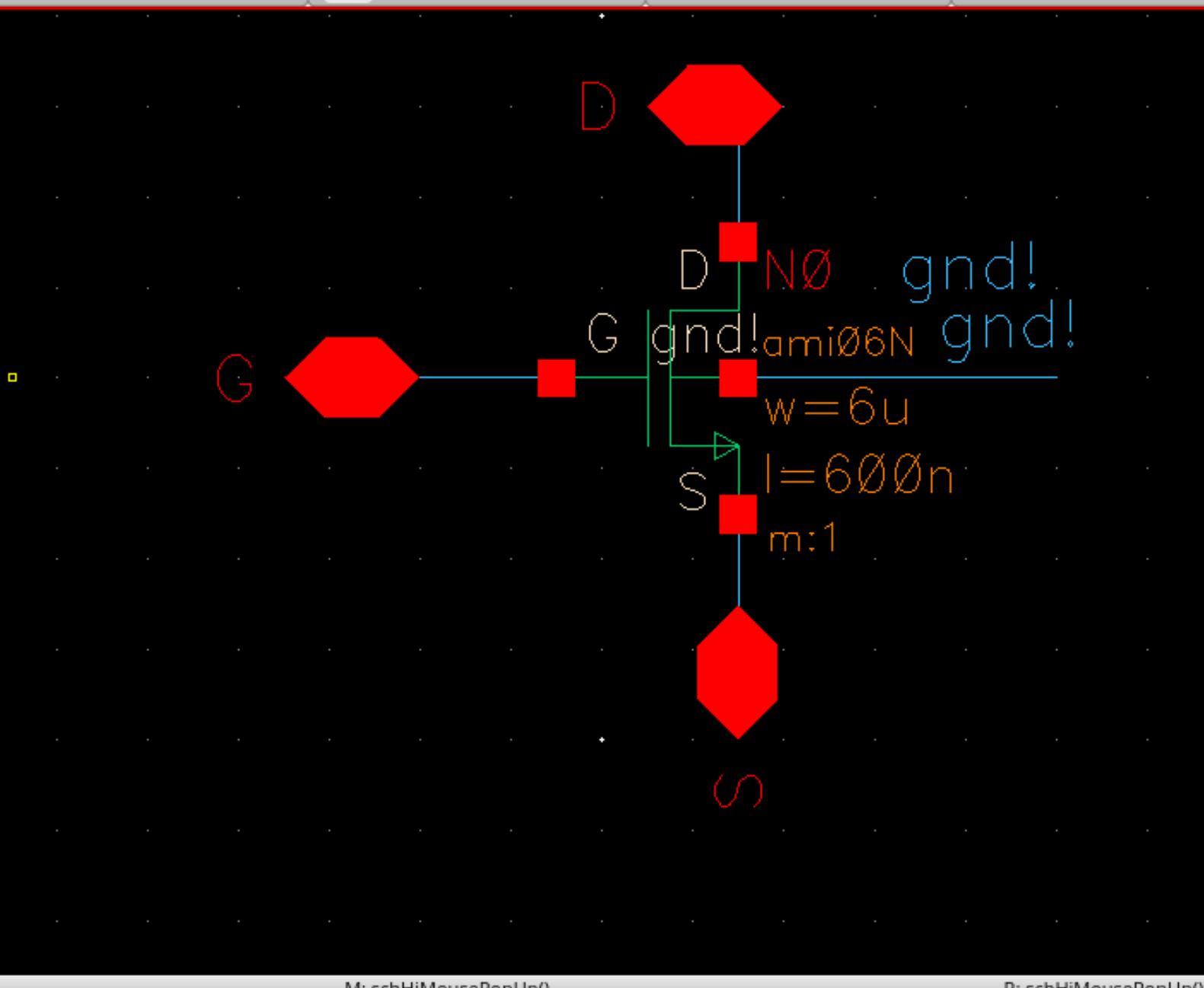
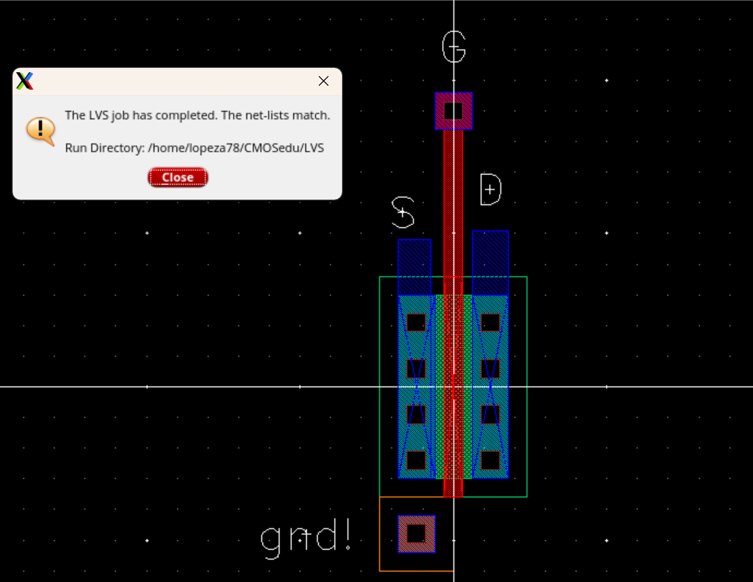
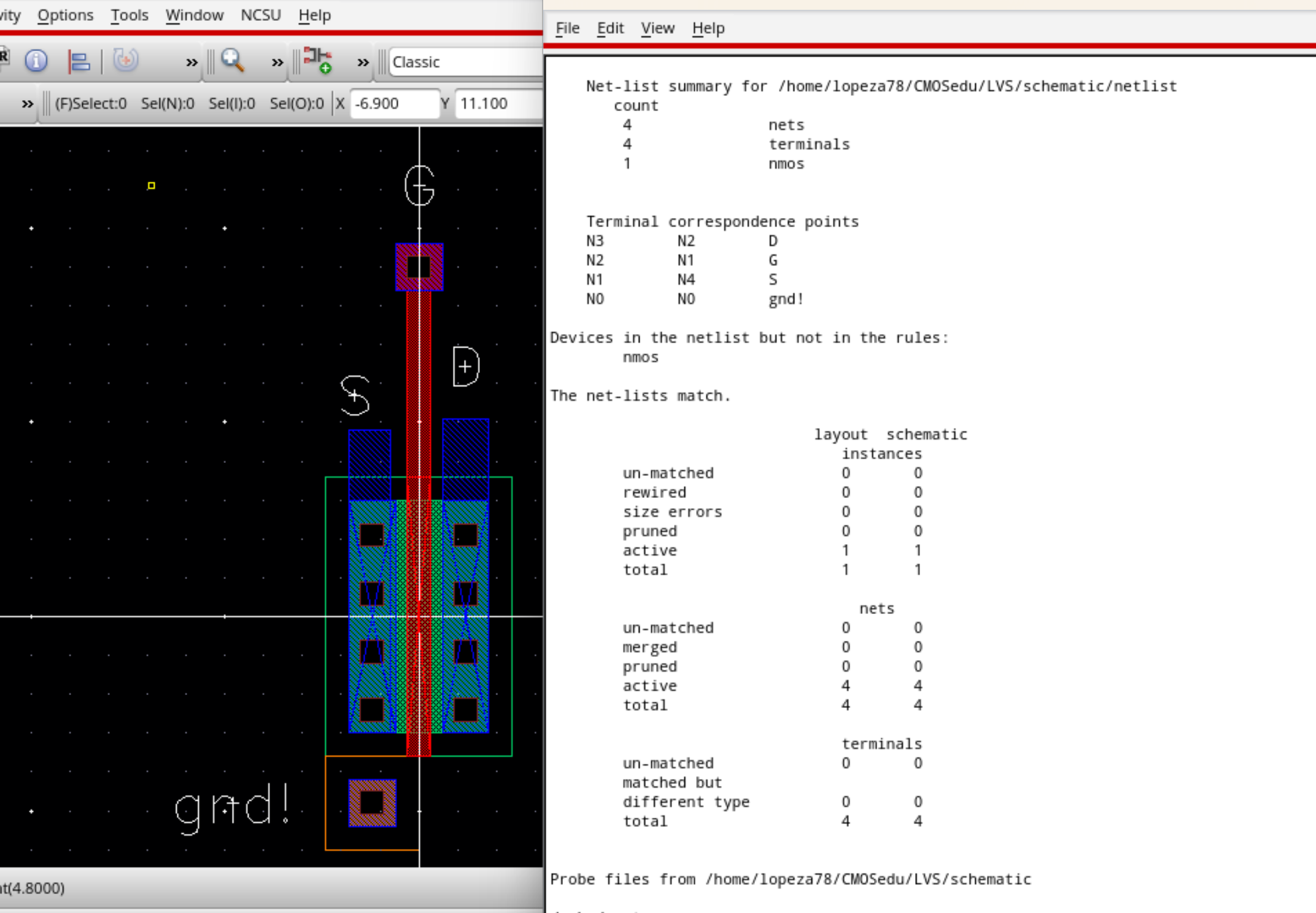
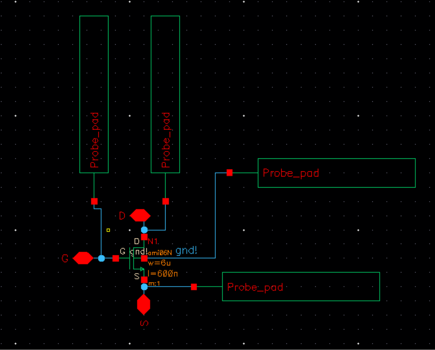
- Make a corresponding schematic so you can LVS your layout. First is my schematic then my LVS
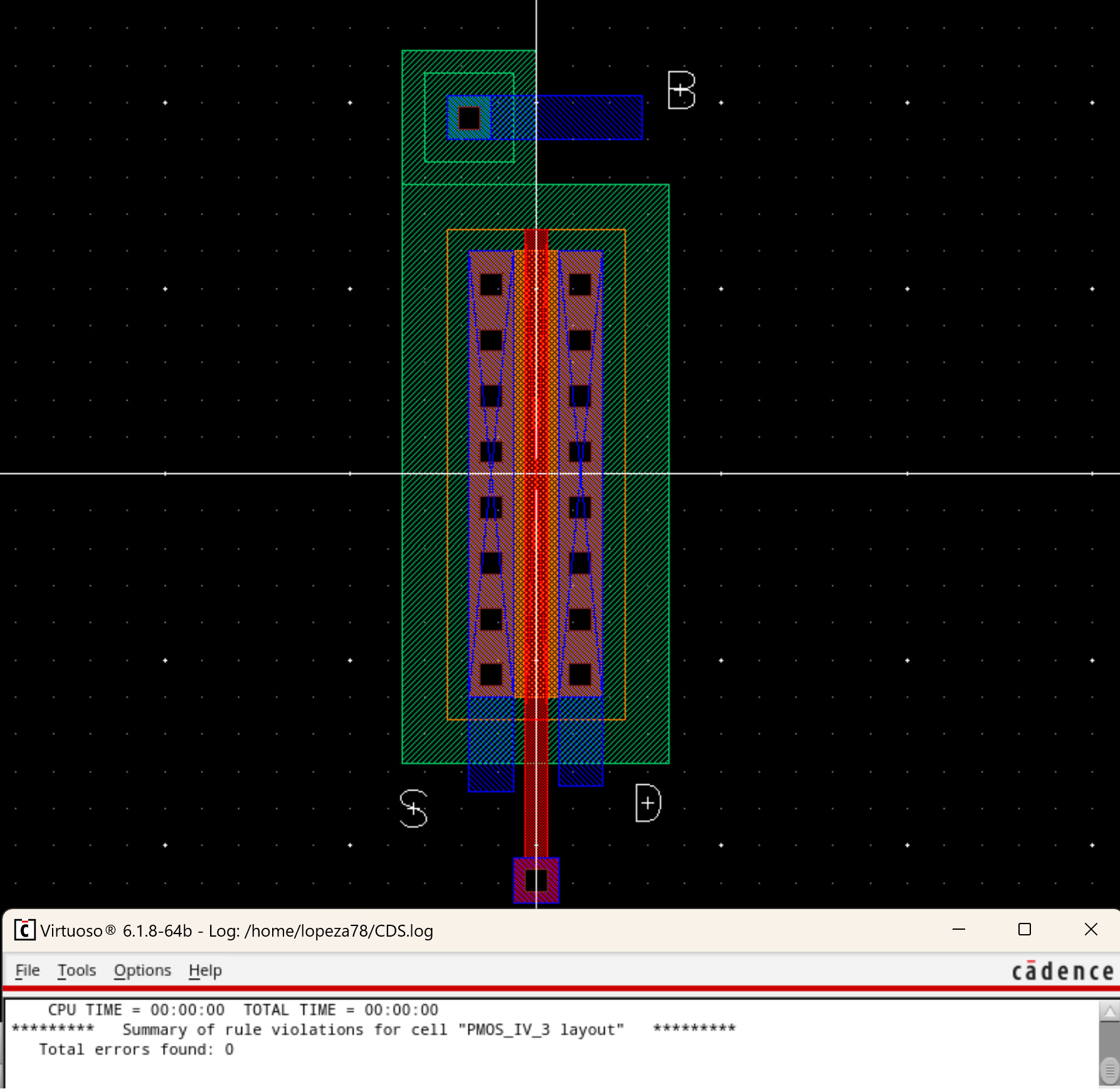
- Lay out a 12u/0.6u PMOS device and connect all 4 MOSFET terminals to probe pads.
- Show your layout passes DRCs.
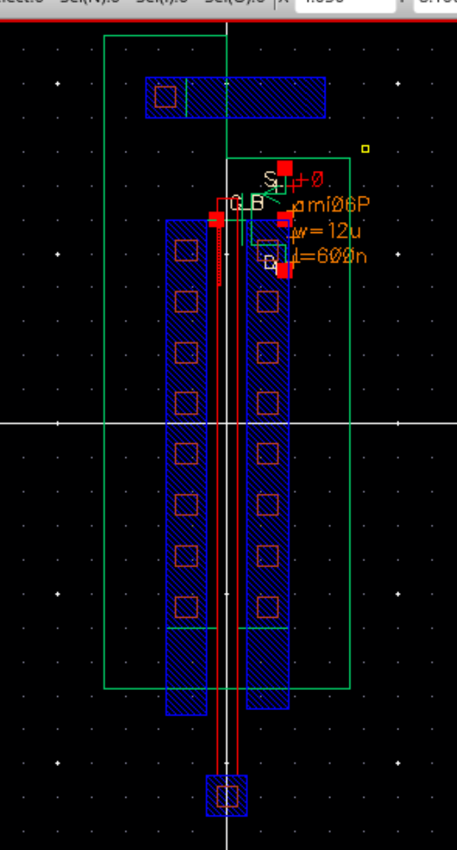
- Make a corresponding schematic so you can LVS your layout.
- Here is the final design directory for my lab.
Return