Lab 3 - EE 421L
Authored
by Anthony Lopez
Email: lopeza78@unlv.nevada.edu
Due Date: September 20, 2023
Lab Description:
- Three main objectives:
- Designing an n-well with proper dimentions.
- Using this n-well as a resistor then creating a voltage divider.
- Incorperating
the voltage divieder layout to create a 10 bit DAC. Then verifying our
layout results to our previously made shcematic.
Pre-Lab:
-
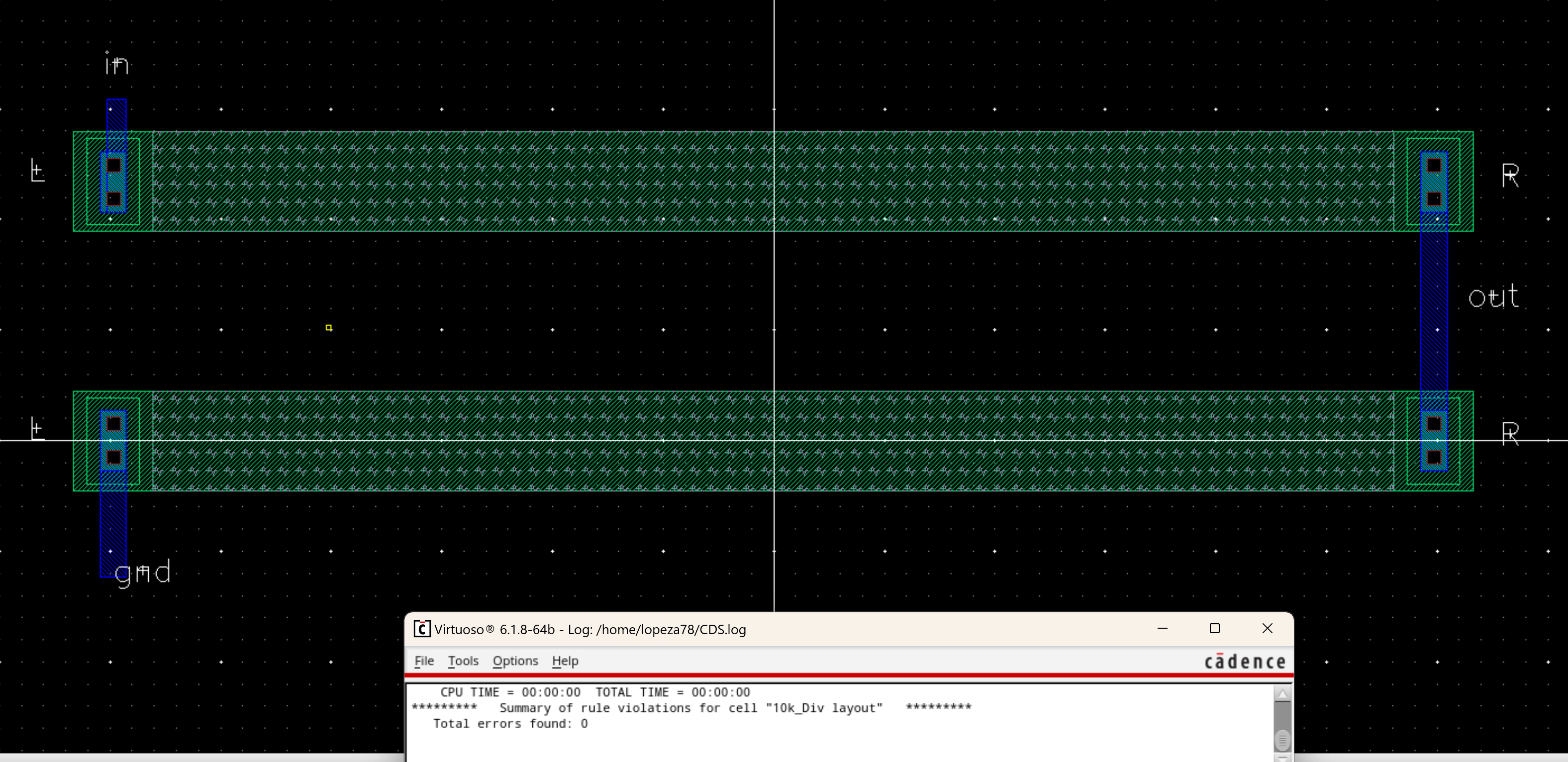
From following the tutorial I ended with this layout and
with no errors. Then the following is the extracted value which is
R=10.21ohms.


-
Continueing the tutorial, I made a layout for my n-well voltage
divider and created the proper pins. Then saved and DRC this layout.
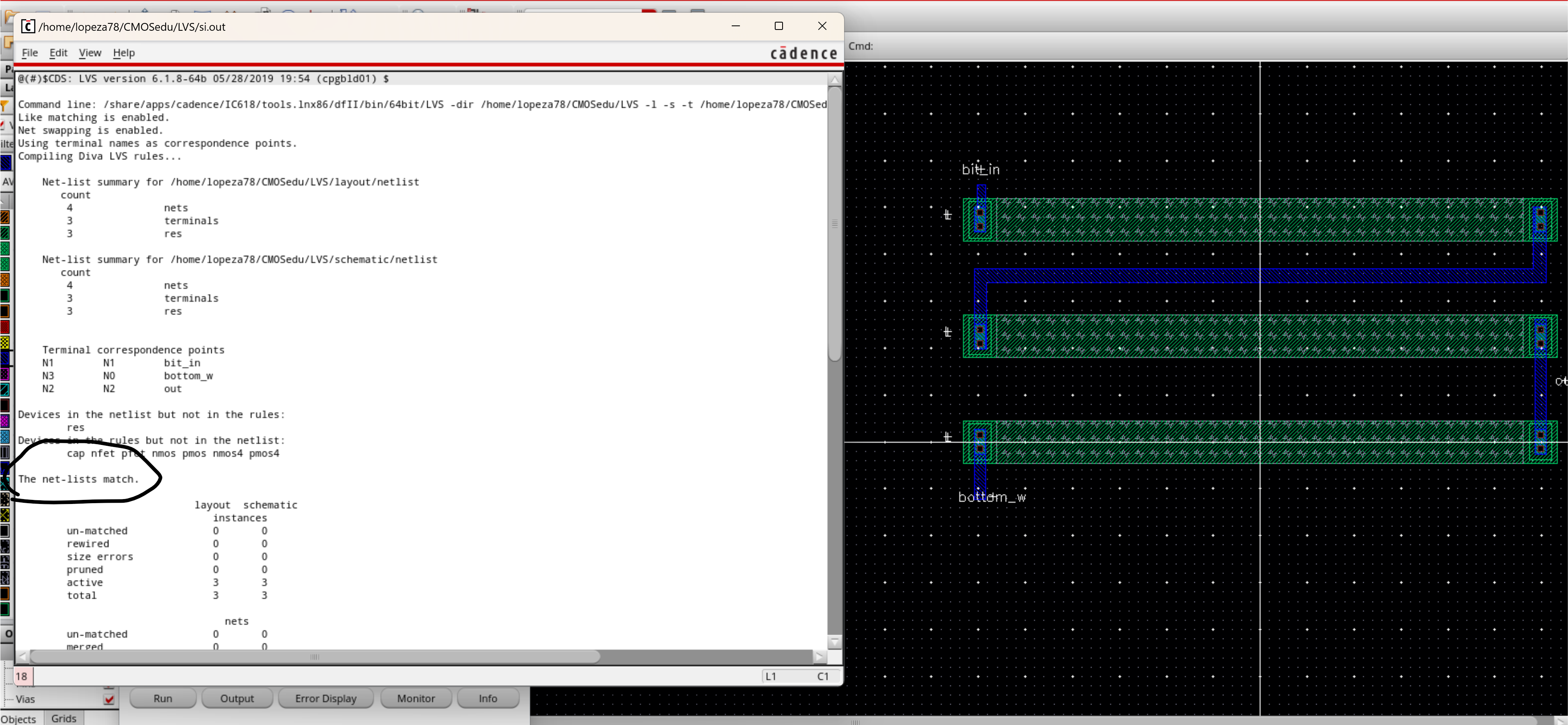
Once that is finished I now extract the layout to then perform LVS the
layout with the voltage divider schematic. However I realized I was
comparing it with the schematic for our DAC and that has two resistors.
Thus i added a well and made the metal connections to accurately
represent the schematic.


-This concludes our prelab.
Lab Tasks:
- Designing the well.
- To
find your width you and length you must have three values to start.
Minimum width, sheet resistance and your desired resistance. The min
width and sheet resistance comes from data sheets or are installed
parameters based on your program. Then your desired reistance is just a
value you choose.
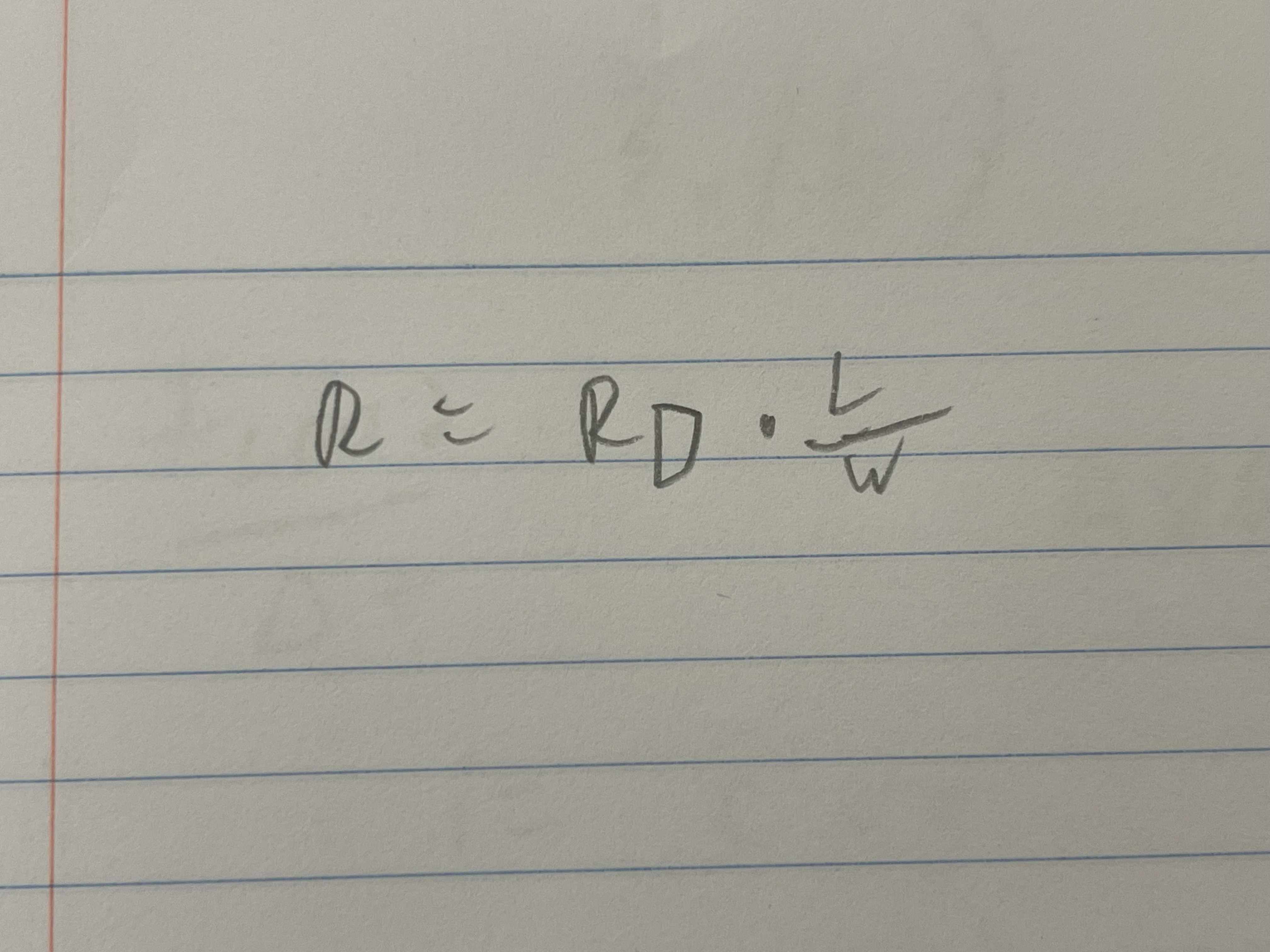
- From these values we use the following equation

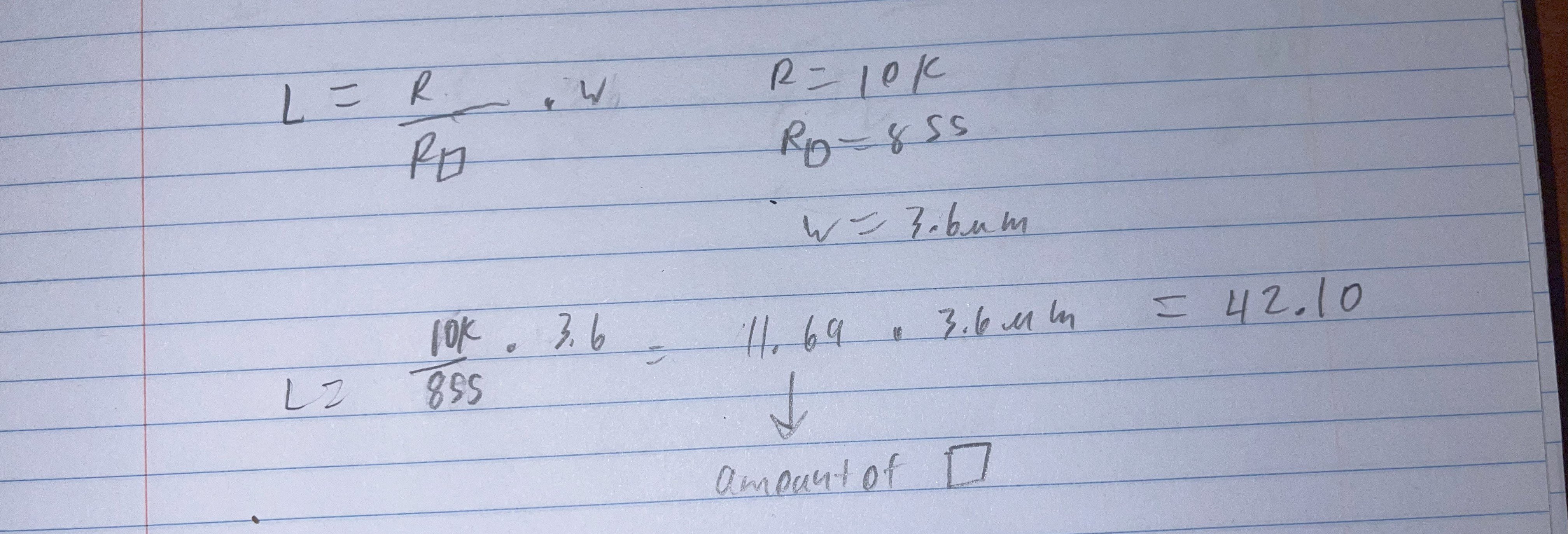
- As we said above you have three of these values so you solve for length can plug in 855 for sheet resistance and then 3.6micro m
for width and 10k for our desired resistance. However, its important to
note that just dividng desired R by R square(sheet resistance) you get
the number of sheets you need. Thus if you change your width for some
design reason, while still remaining above the min, then your length
will change as well. Such as with my design where I followed the
tutorial and made my width 4.5 thus resulted in a longer length.

- From
here we can then ensure our well is the desired lenght by measuring
through the k key bind which when pressed will bring up a ruler tool as
shown below. However it is important to note that your ededges must be
on the grid which are spaced out about 1 micron. Thus if any errors
occur with the edge then you just adjust your length to ensure they
snap onto the grid.

- Desiging the DAC
- Now
that I have a voltage divider made of n-wells, I will be using this
layout to design my DAC. I made a new layout so then I can keep this
divider available for other layouts. I brought in the layout I just
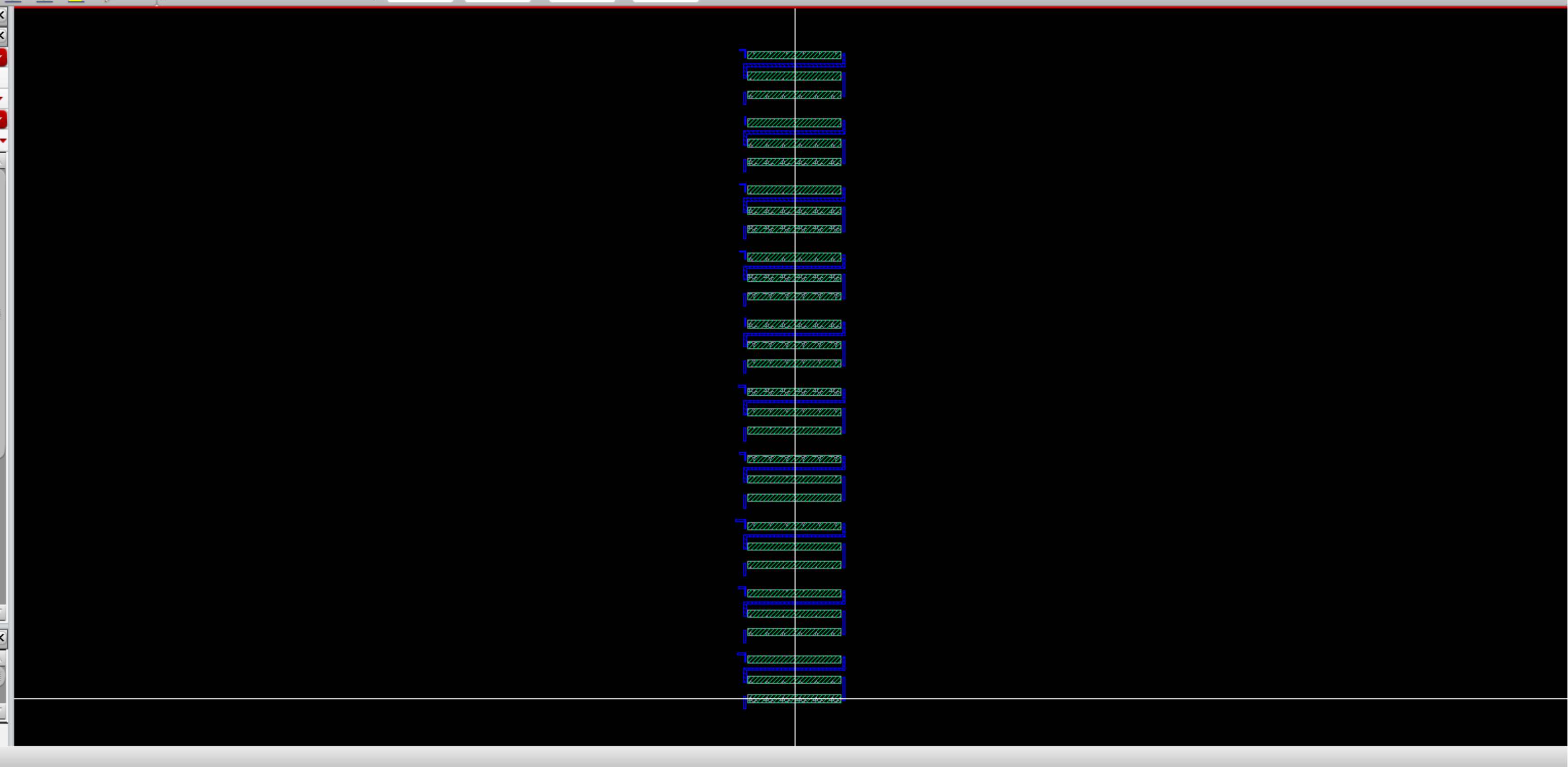
created then made 9 more copy of these three resistors to represent
each bit of our DAC.

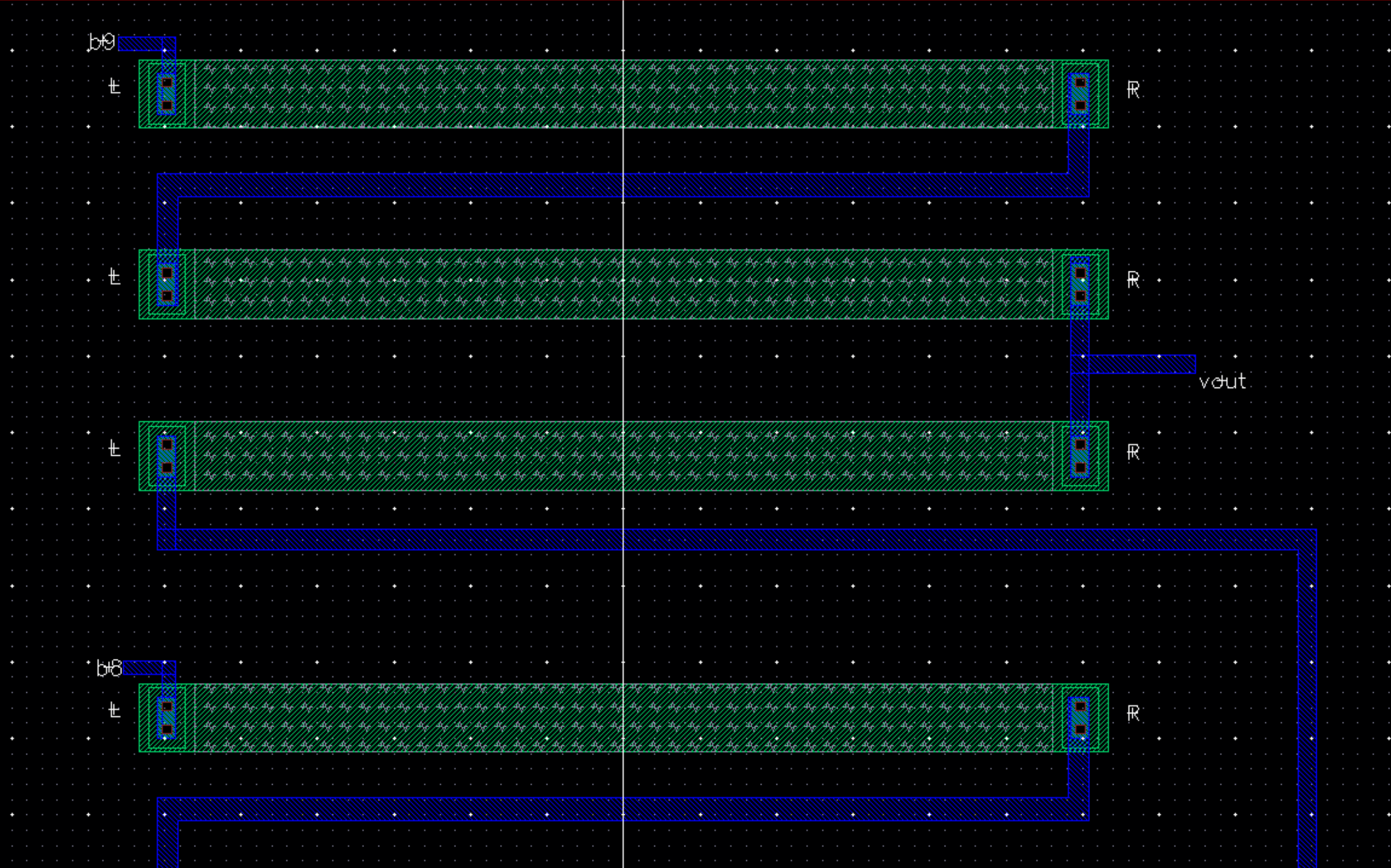
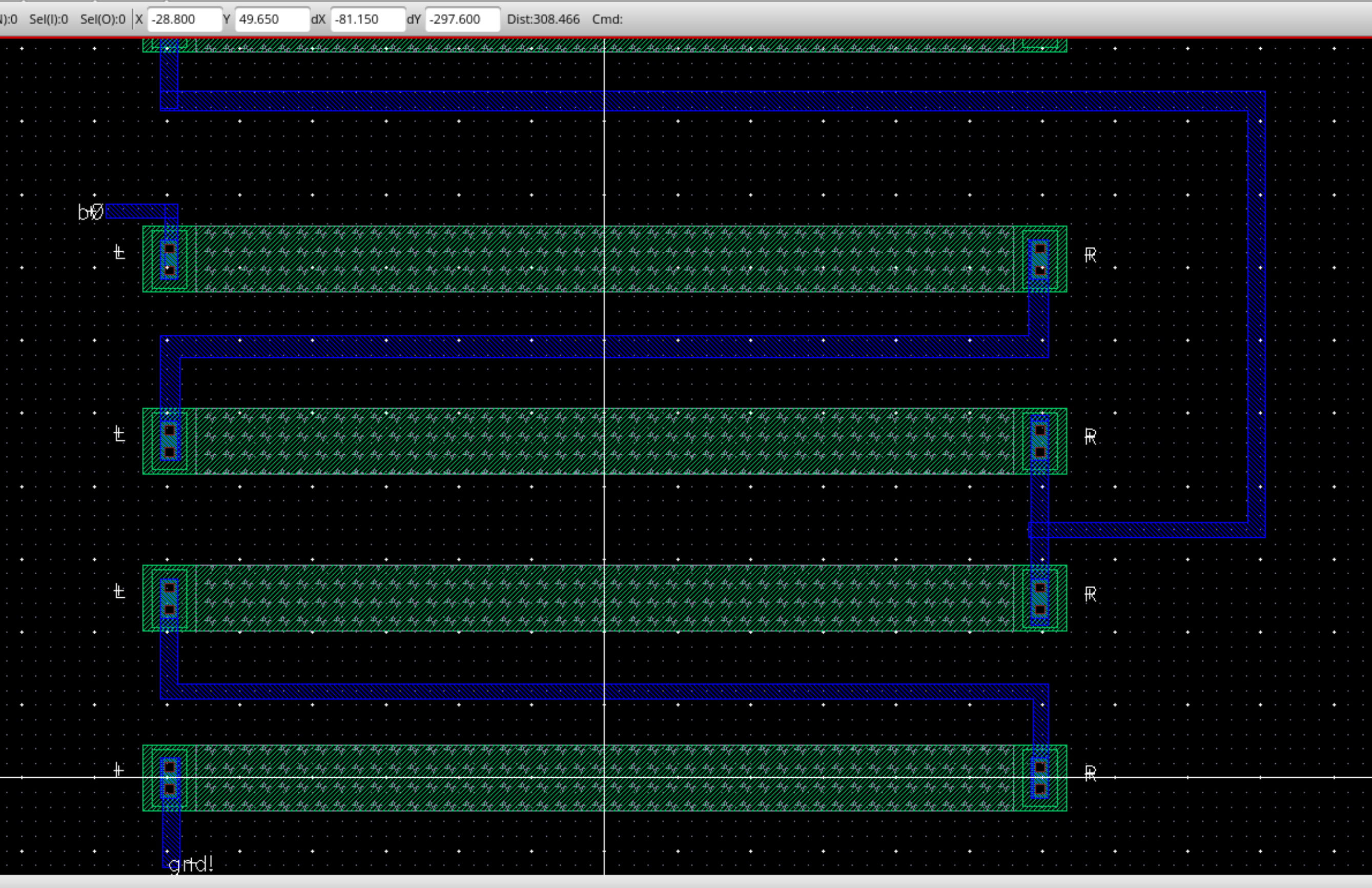
- From here I made the proper pins and connections from one divider to another using metal 1. First image is a close up of the top two bits and bottom is b0 and ground.


- DRC and LVS
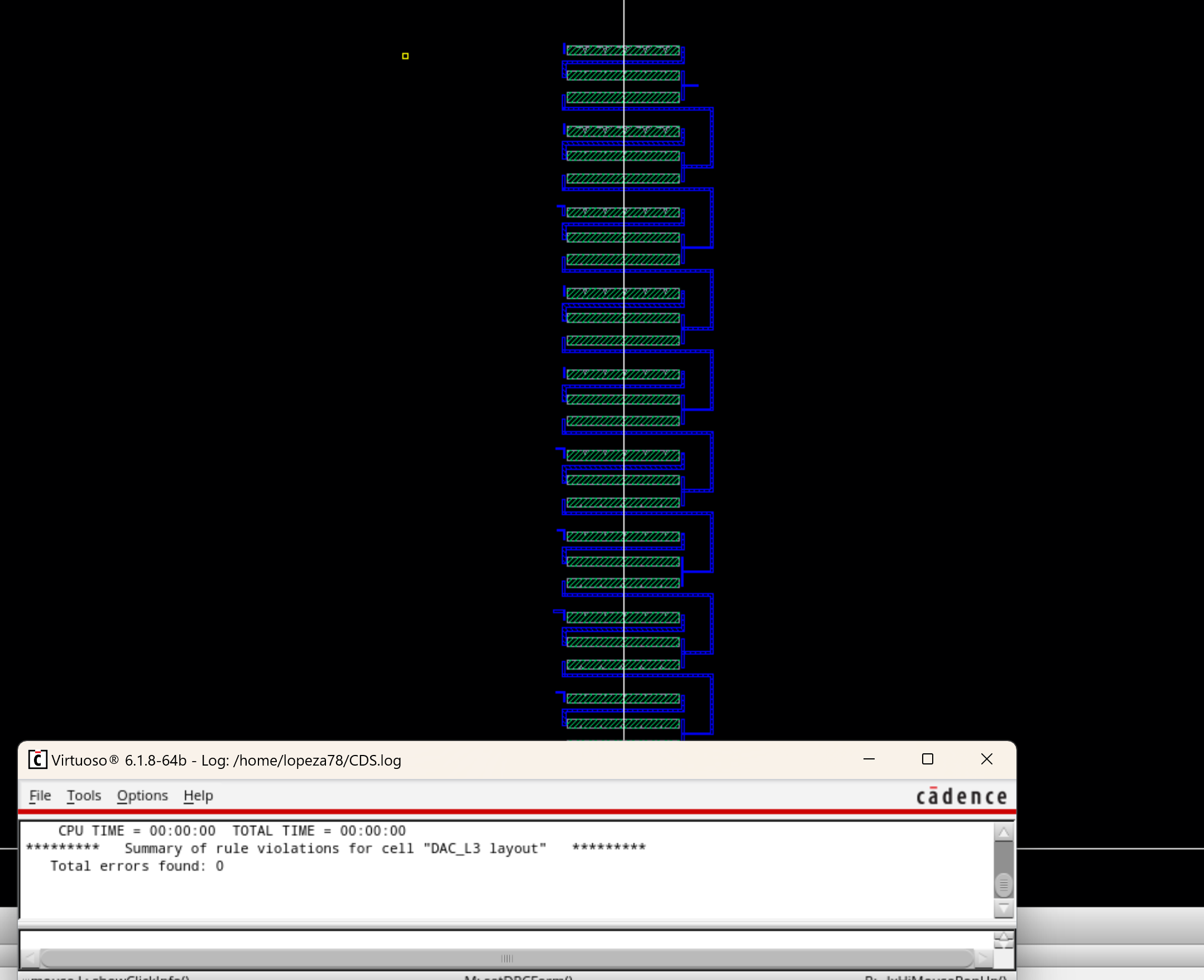
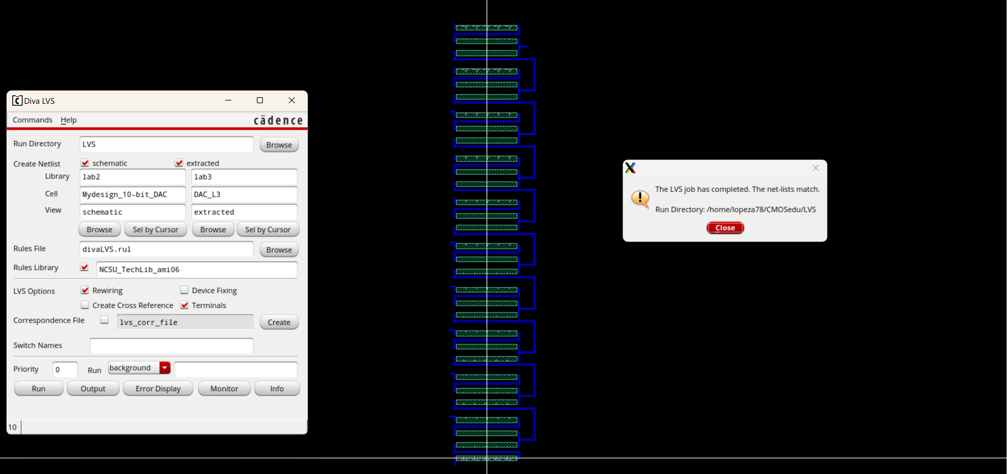
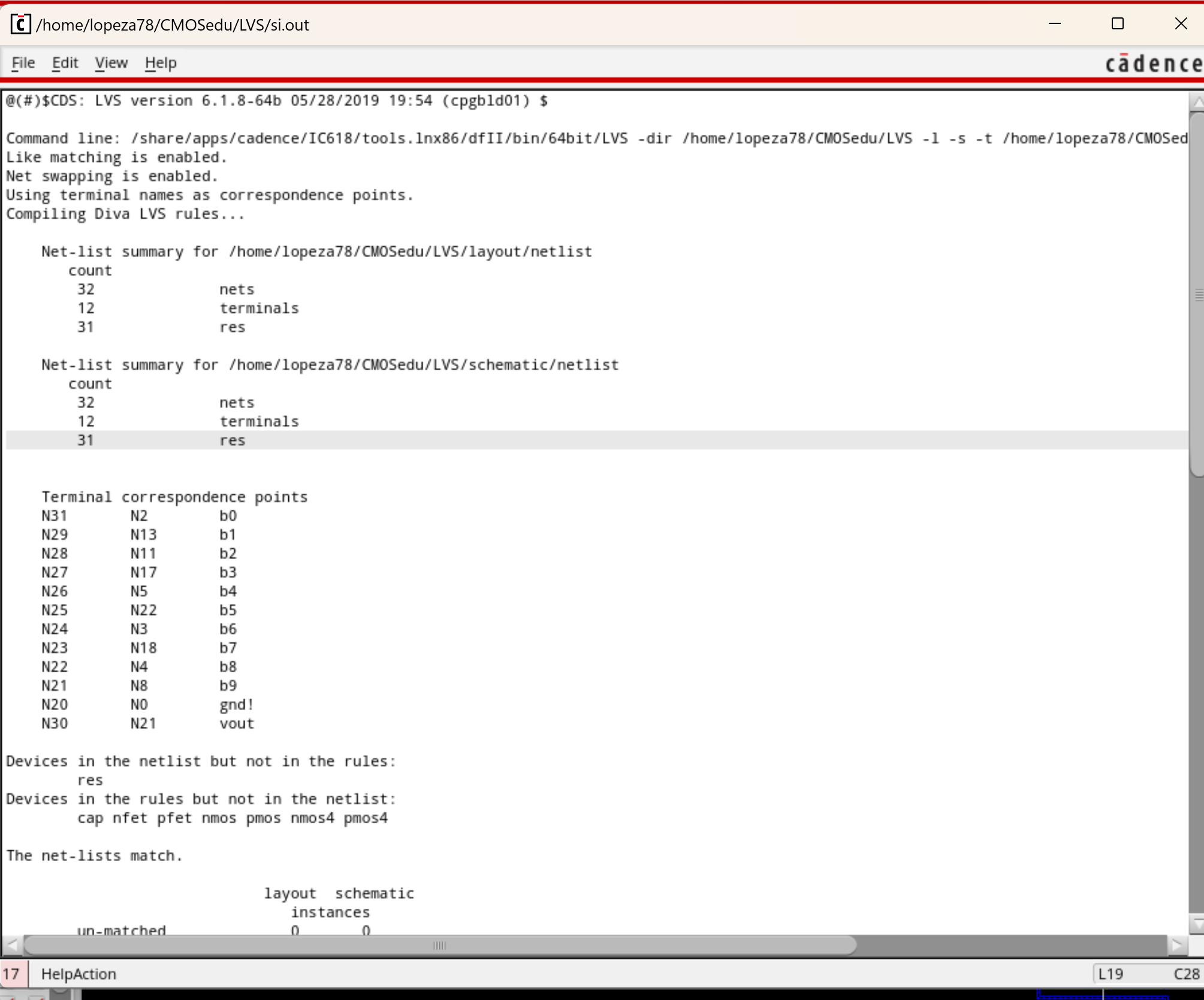
- Here I will display my results for DRC of layout and my LVS respectively.


- Here is the final design directory for my layout and schematic. Schematic and layout.
Return
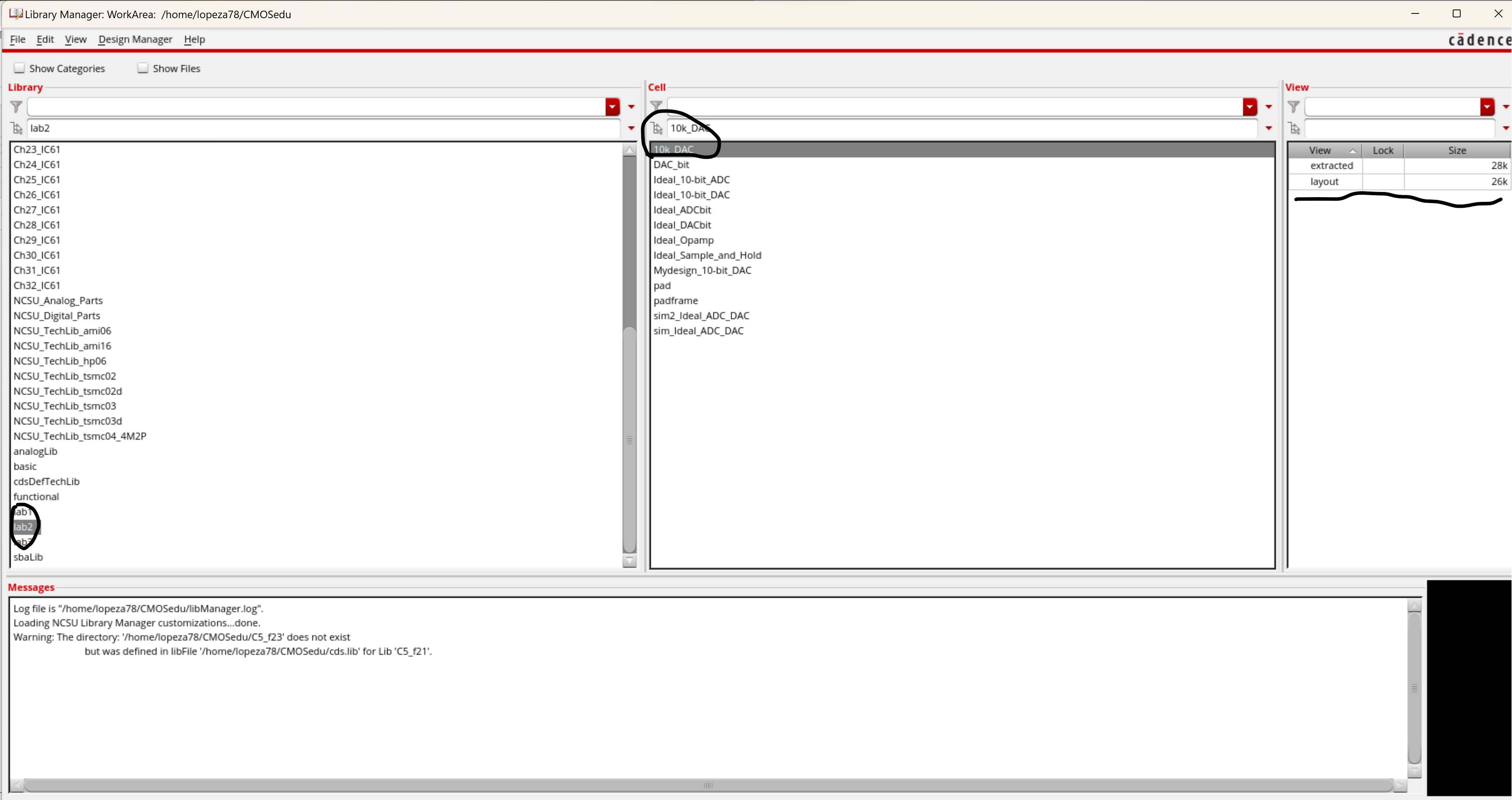 -Then I made a copy for lab 3 and renamed thie cell in lab 2


