(an output logic 0 is near ground and an output logic 1 is greater than 7V).
Assume
VDD is between 4.5V and 5.5V, a valid input logic 0 is 1V or less, a
valid input logic 1 is 3V or more. Show that your design works with
varying load capacitance from 0 to 1 pF.
Assume the slowest transition time allowed is 4 ns.
Notice
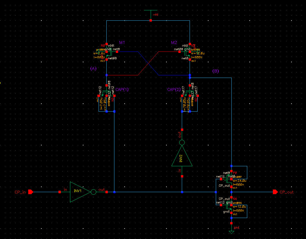
in the schematic that Node (A) does not supply any power to the output.
It's only purpose is to turn on M2 thus allowing node (B) to be
precharged to VDD when the input is a low.
For the next cycle we will achive an output voltage closer to our 2VDD that we desire.
To achive this we calculate it two ways first is by finding the max width of our NMOS
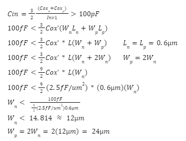
- Determining our max widths given we are using min lengths of 0.6 micro meters
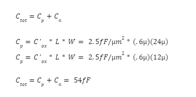
- Total Input Capaciatance of Inverter:
- Inverter schematic and symbol
2.) Circuit Design
- Choosing nmos and pmos sizes
For my sizes of Pmos and Nmos I first started by using the exampled provided from the book figure 18.39
while following the contraints in Figure 32.8 which stated i should follow a sizing of 240/1 for my Pmos and
80/1 Nmos. After pluging those values in with the multiple of 0.6 to follow C5 design I realized I exceeded
the limit set for input capacitance of 100pF by 188pF so I scrapped that way and went with the math listed
above. I began by setting all my Mosfets to the the same 24/12 ratio calculated above simply to start with logic.
- Choosing C1 and C2
For choosing C1 and C2 I decided to use Nmos's in place of capatitors
to save space on the layout as the
NMOS's would be in strong inversion. Strong inversion accurs when a large quantity of electrons attach
under the gate noted and the capacitance will increase. The build up of electrons will short to the drain
and source. This forms a low resistance "bottom plate" forming a capacitor.
In order to keep the MOSFET in strong invertion Vgs (Voltage differeance between the gate and source)
> Vth (Threshold Voltage). Since we are in C5, the threshold voltage is 0.7V.
Due to the contraints of our project the lowest our VDD can be is 4.5V allows us to to keep a constant
differance greater than the Vth arcross the MOSFET. For calculating the actual sizes:
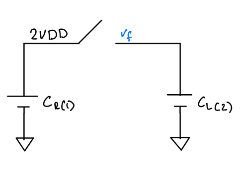
(Cr(1) refers to CAP(1) ; Cr(2) refers to CAP(2) in schematic)
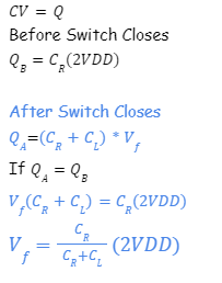
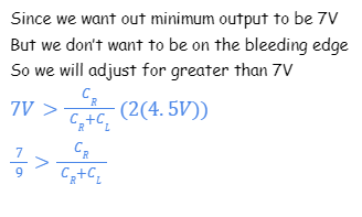
At this point we can tell that we can pretty much chose any thing that is greater than this ratio of 7/9.
In my first version of the project I implement
C1:25pF
C2:250fF
while this works it also takes up a large amount of space in layout so we adjusted down to
C1: 12.25pF
C2:122.5fF
Which gives us a ratio of about .9917 which fits the constraints.
- Choosing M1 and M2
This was a trivial task as all what was important was that we make M1 smaller than M2 for this I
made M1 1/5 of M2. This is done to minimize layout area and power.
3.) Switching point logic check
- A valid input logic 0 is 1V or less
- A valid input logic 1 is 3V or more
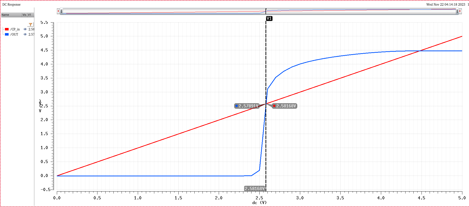
- At 4.5V VDD
- At 5.0V VDD
- At 5.5V VDD
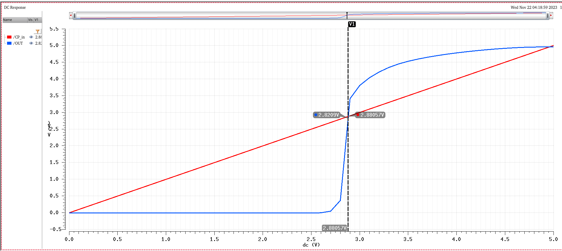
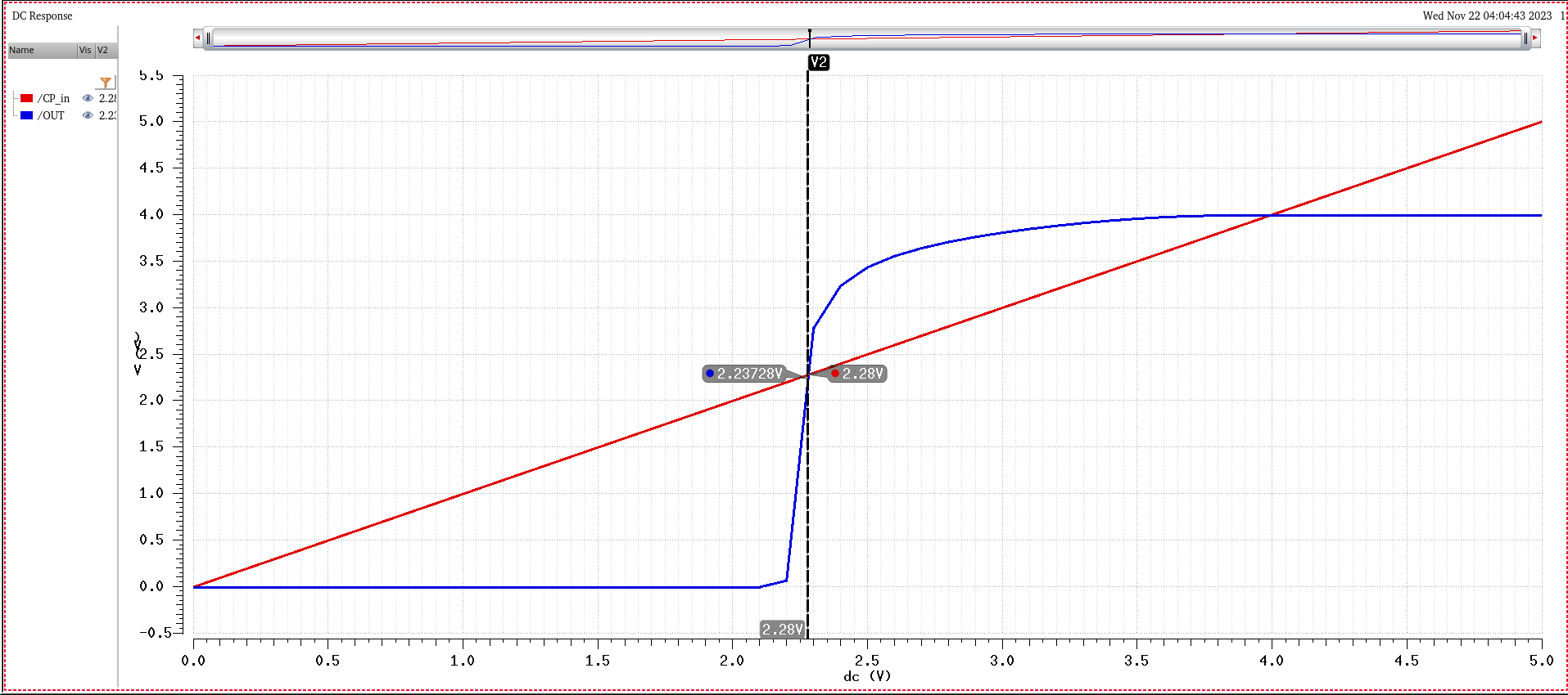
- Our switching point ranges from 2.23V to 2.88V which is well with in our logic perameters.
- Switching point
We got "lucky" when determining this by design perameters we can use the following equation
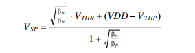
This describes the relationship between the size (Width and Length) of the Nmos in relation to the Pmos.
If we wanted to shift our switching point to the left say lower our range we make the Nmos width bigger.
Assuming they share the same length.
If we wanted to move our range up say 4V is now considered logic 1 then
we would have to increase the size of the Pmos.
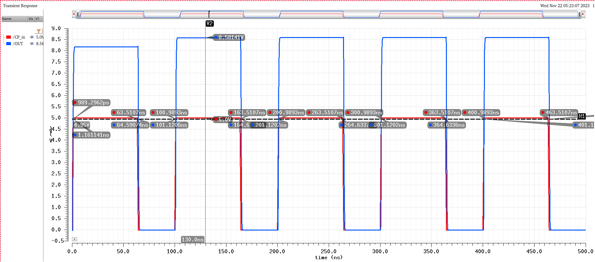
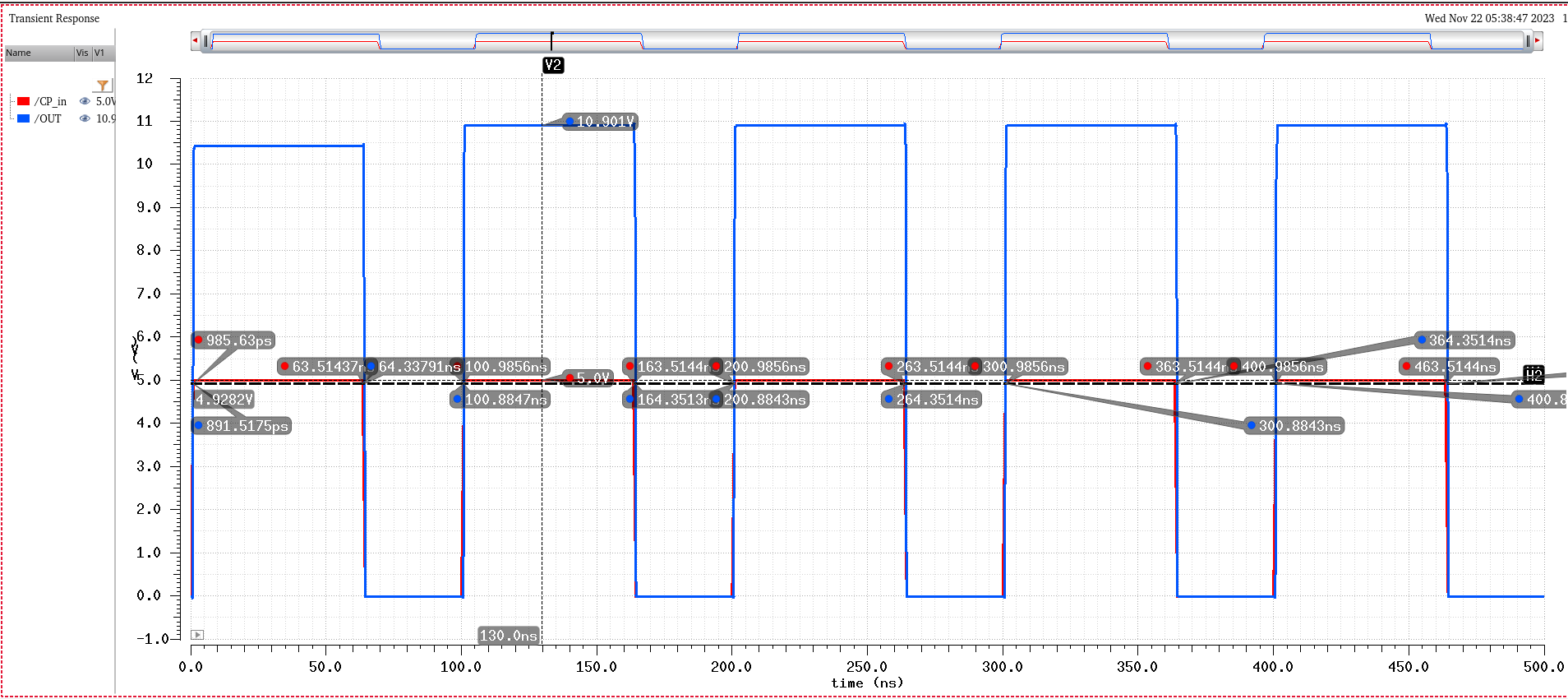
4a.) Testing at 4.5V (No Load)
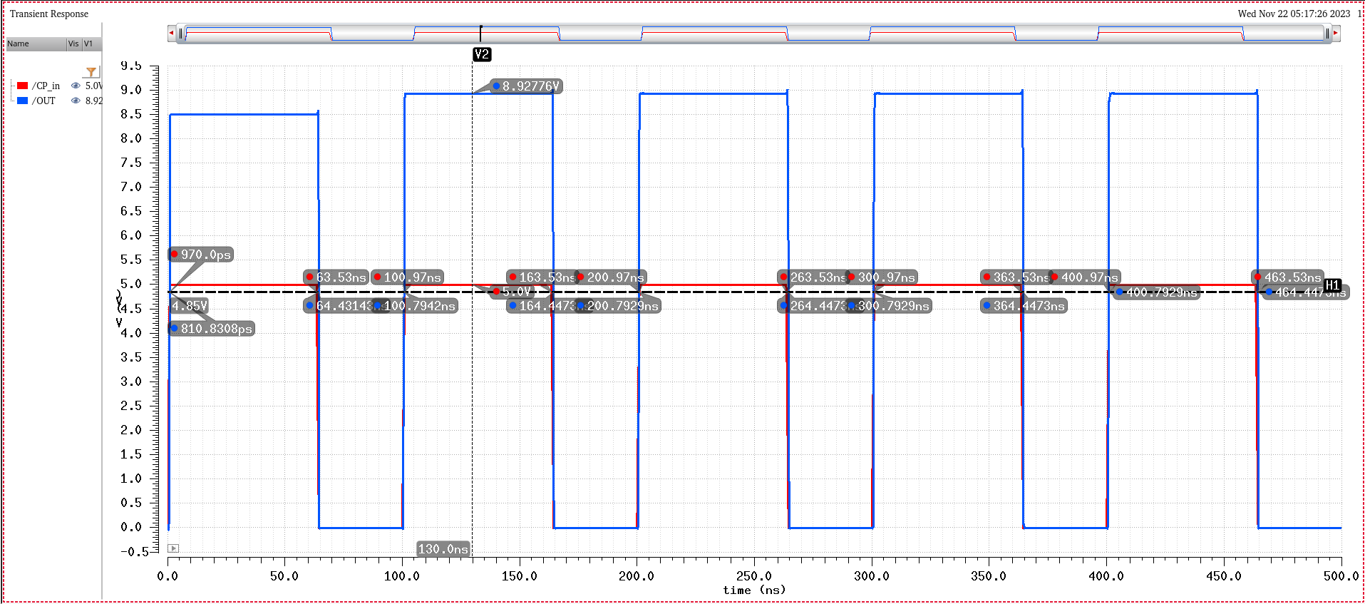
Time Delay (Low to High) = 177.1pS
Time Delay (High to Low) = 917.3nS
Time Total = 1.094nS
4b.) Testing at 4.5V (0.5pf Load)
Time Delay (Low to High) = 130.7pS
Time Delay (High to Low) = 1.1229nS
Time Total = 1.3597nS
4c.) Testing at 4.5V (1pf Load)
Time Delay (Low to High) = 430.6pS
Time Delay (High to Low) = 1.1242nS
Time Total = 1.6548nS
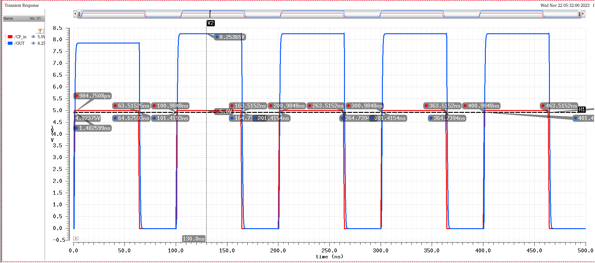
5a.) Testing at 5.0V (No Load)
Time Delay (Low to High) = 140.9pS
Time Delay (High to Low) = 877.1pS
Time Total = 1.018nS
5b.) Testing at 5.0V (0.5pf Load)
Time Delay (Low to High) = 144.3pS
Time Delay (High to Low) = 1.1049nS
Time Total = 1.2492nS
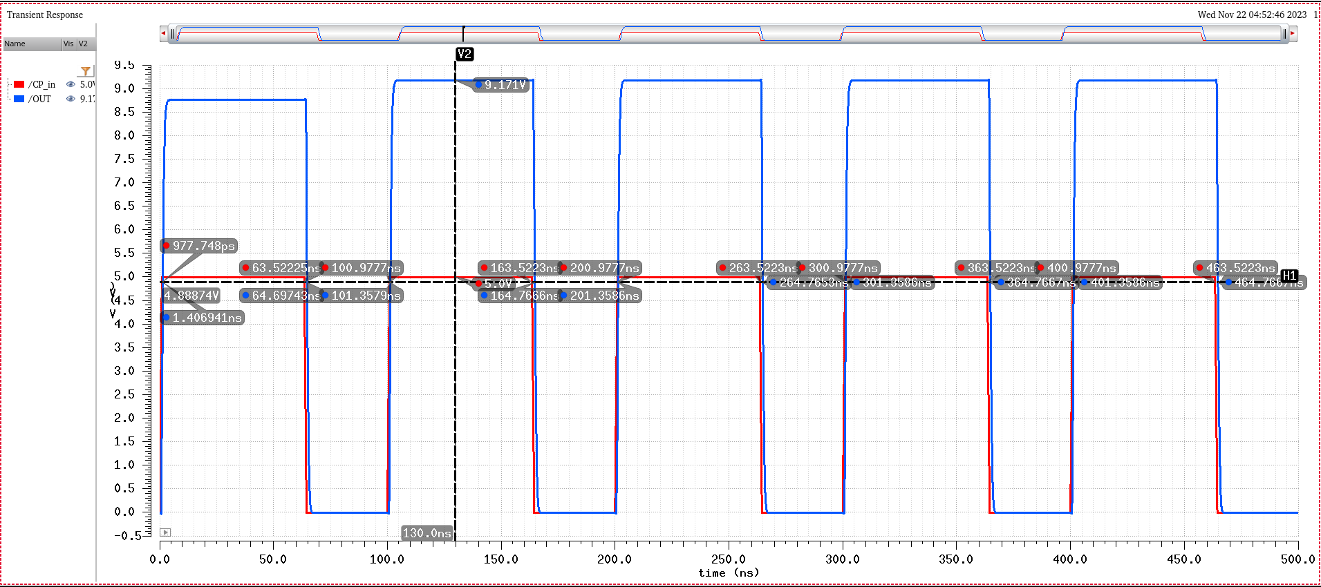
5c.) Testing at 5.0V (1pf Load)
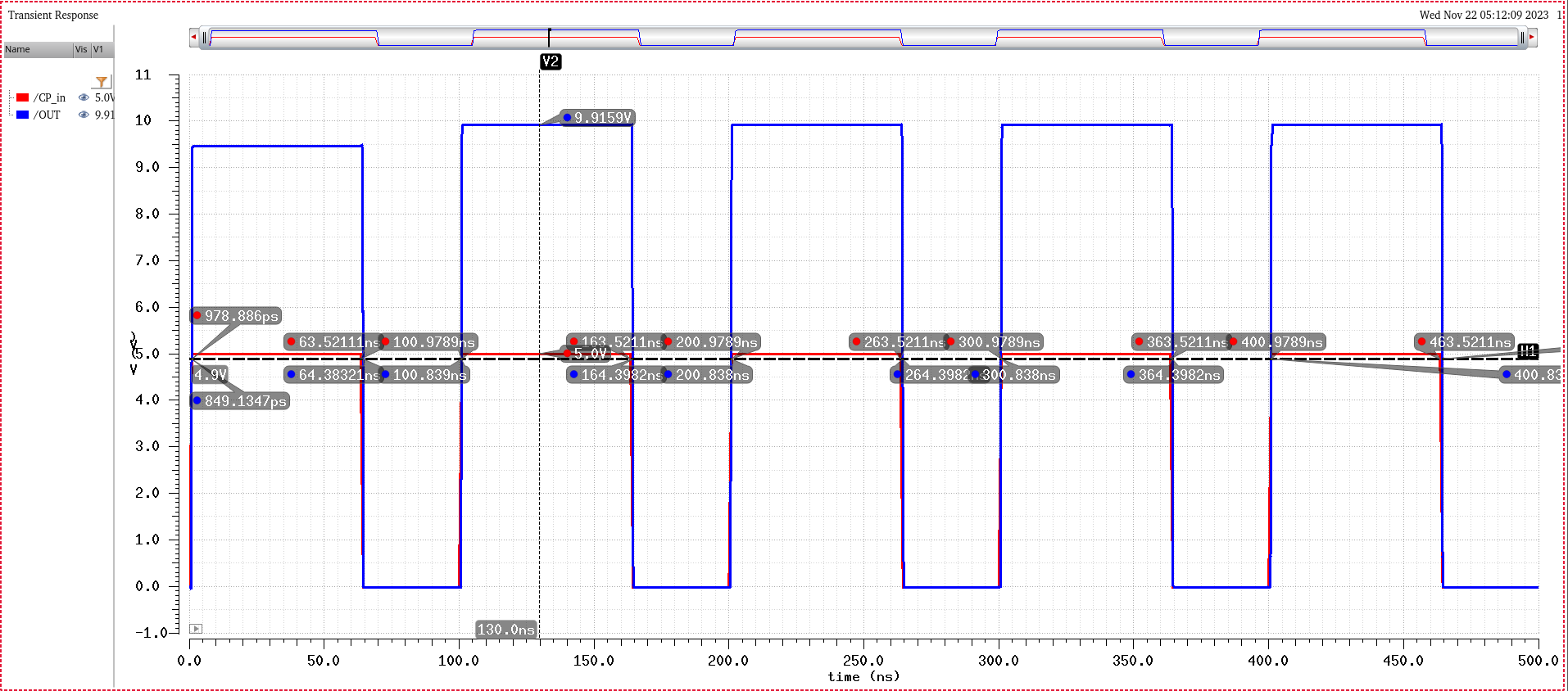
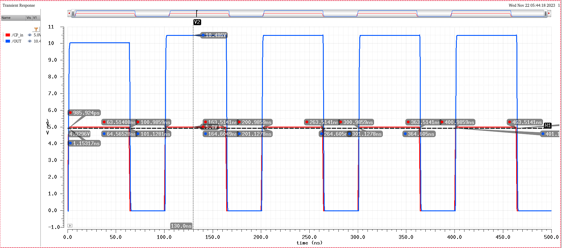
6a.) Testing at 5.5V (No Load)
Time Delay (Low to High) = 101.3pS
Time Delay (High to Low) = 836.6pS
Time Total = 937.9pS
6b.) Testing at 5.5V (0.5pf Load)
Time Delay (Low to High) = 141.9pS
Time Delay (High to Low) = 1.090nS
Time Total = 1.2328nS
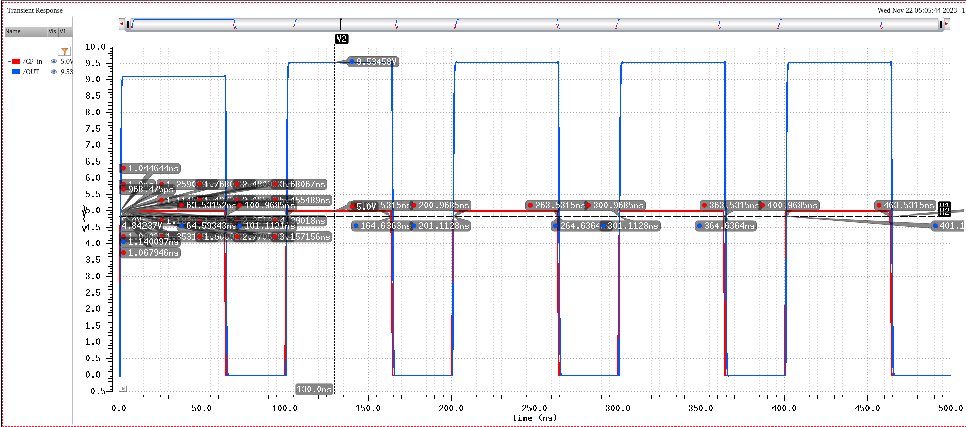
6c.) Testing at 5.5V (1pf Load)
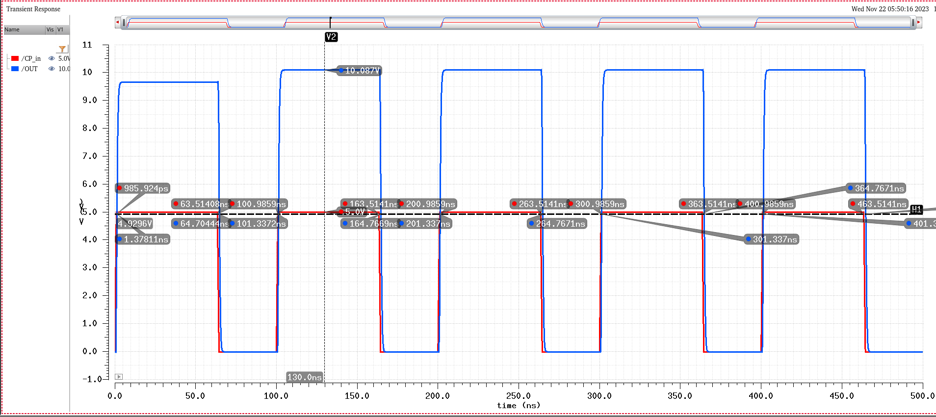
Time Delay (Low to High) = 351.1pS
Time Delay (High to Low) = 1.253nS
Time Total = 1.6041nS
We can notice as the our Cload increase the delay increases and this hold true to our formula that
tdelay = 0.7RC
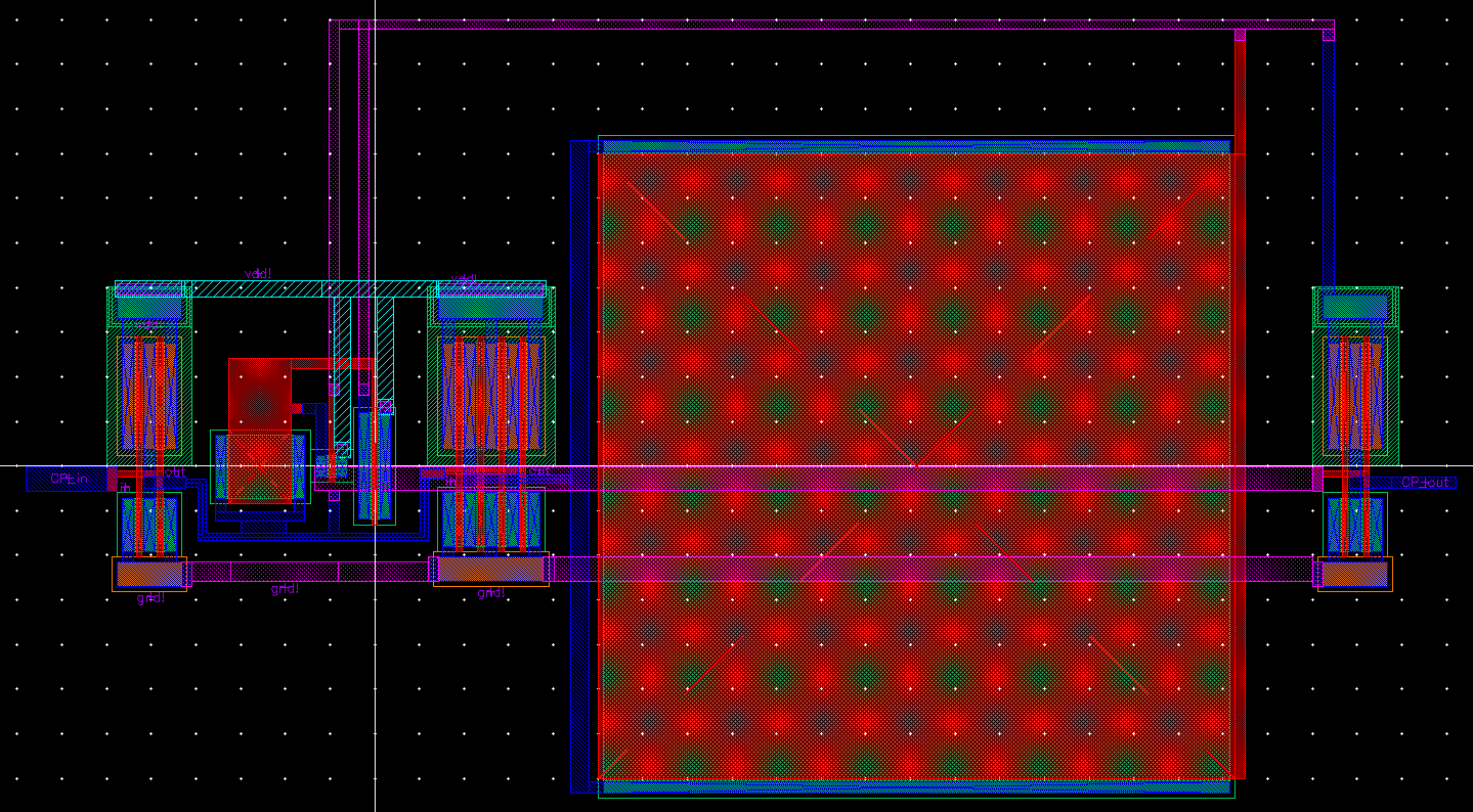
7.) Layout
INV1 LVS and DRC
INV2 LVS and DRC
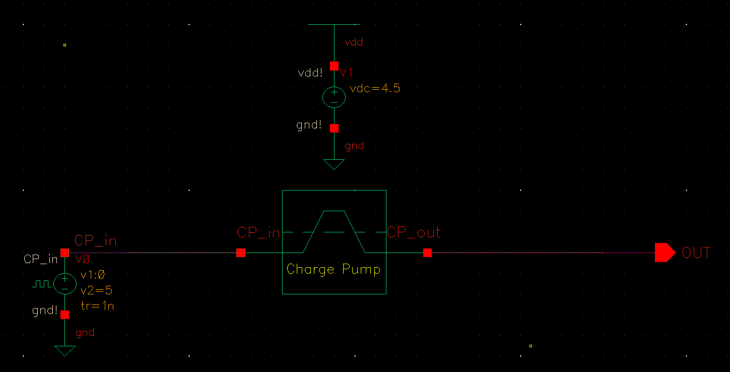
Charge Pump Layout:
While trying to save layout space I organized left to right in order to
keep it easy to understand for the reader.
Along with that I took advantage of the layer system to avoid the
common mistake of trying to keep the metals from overlapping.
-Left most is INV1
-After that comes C1
-Followed by M1
-Next to M2
-In 5th comes INV2
-Connected to that is C2
-Lastly the output inverter.
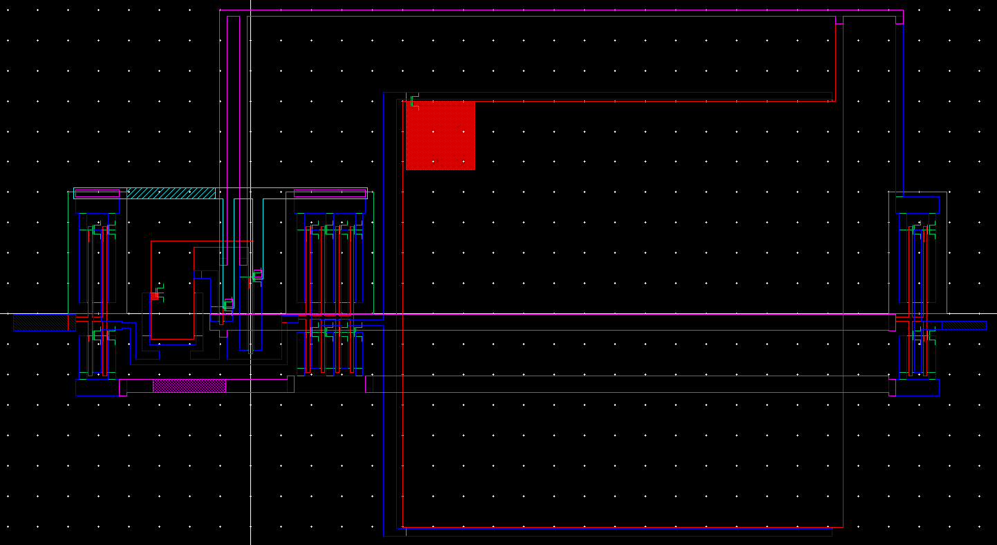
Extracted View
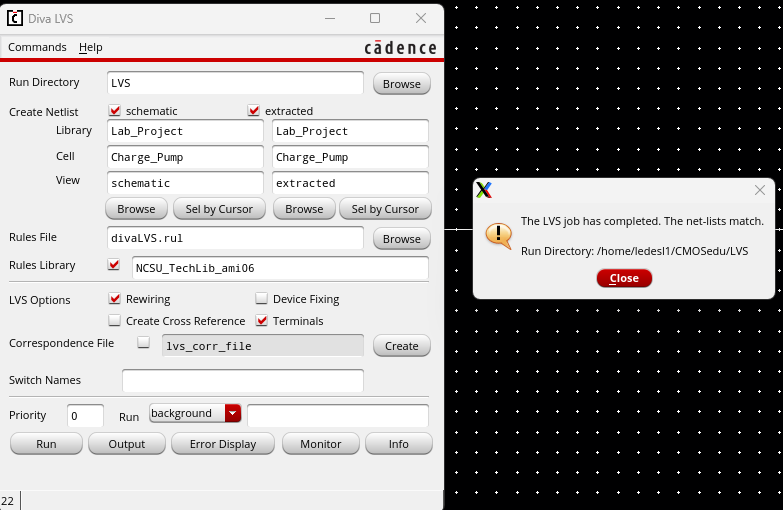
LVS Pass
Files are located here