- This lab will cover the design and simulation of a 10-bit digital-to-analog converter (DAC)
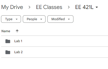
Figure 1: showing the login process and unzipping the lab2.zip file
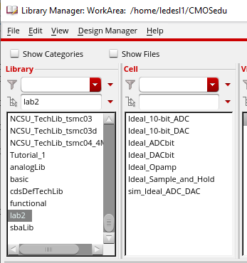
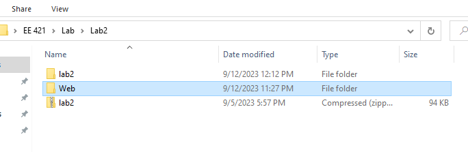
Figure 2: showing lab2.zip added and unzipped in the CMOSedu directory
Figure 3: Showing the edit made to the cds.lib file
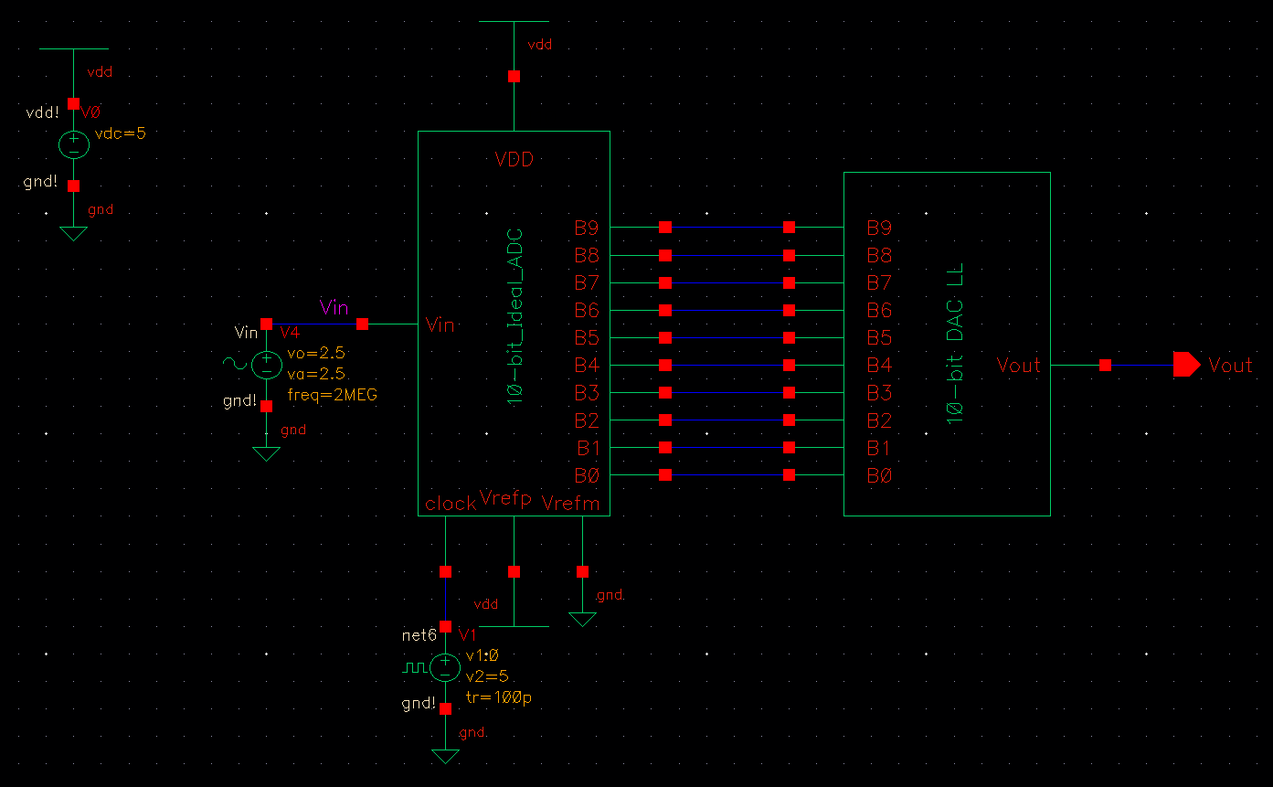
A simulation of the sim_Ideal_ADC_DAC 10-bit ADC and DAC is now performed using the matching ADE L simulation associated.
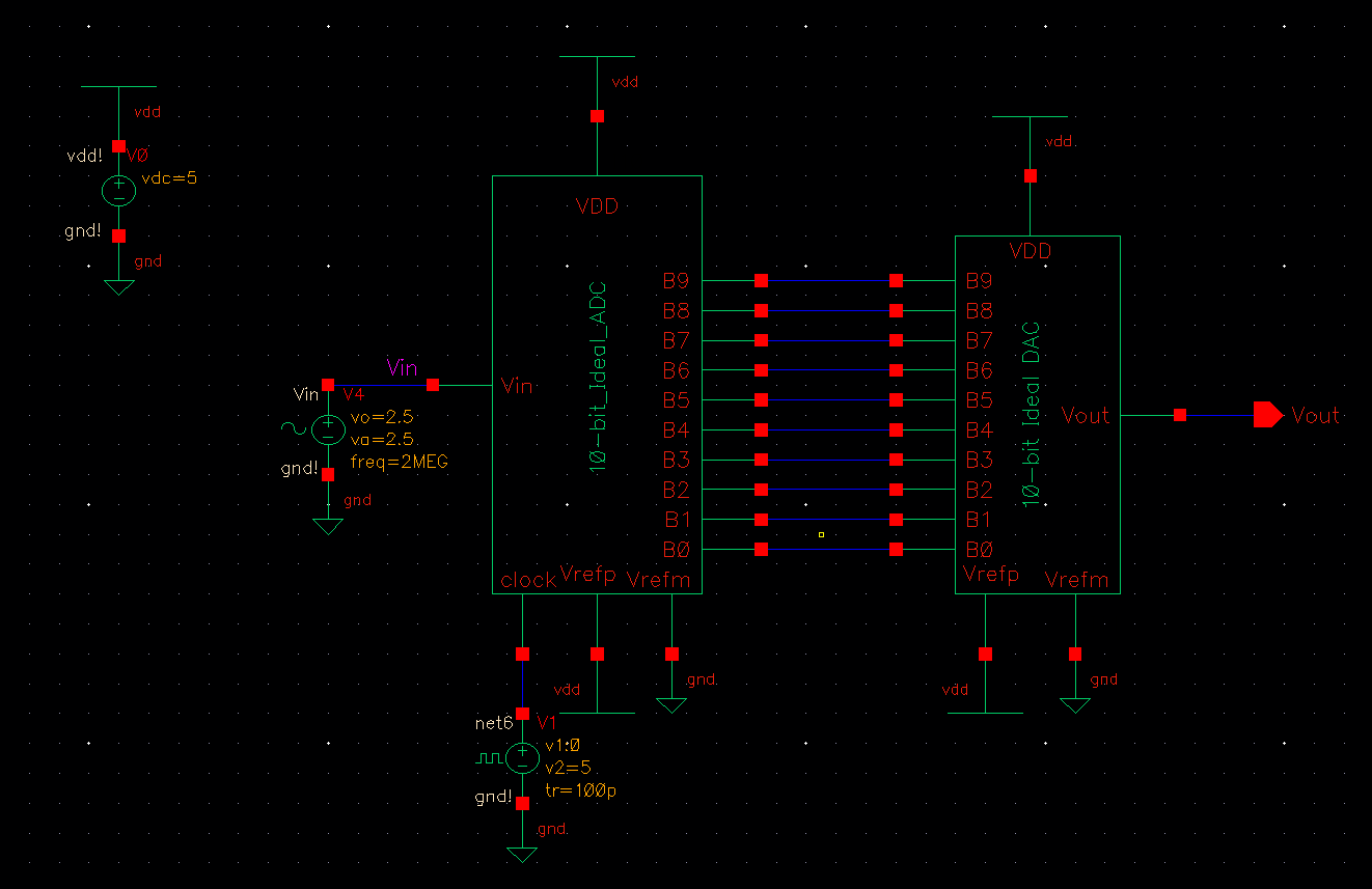
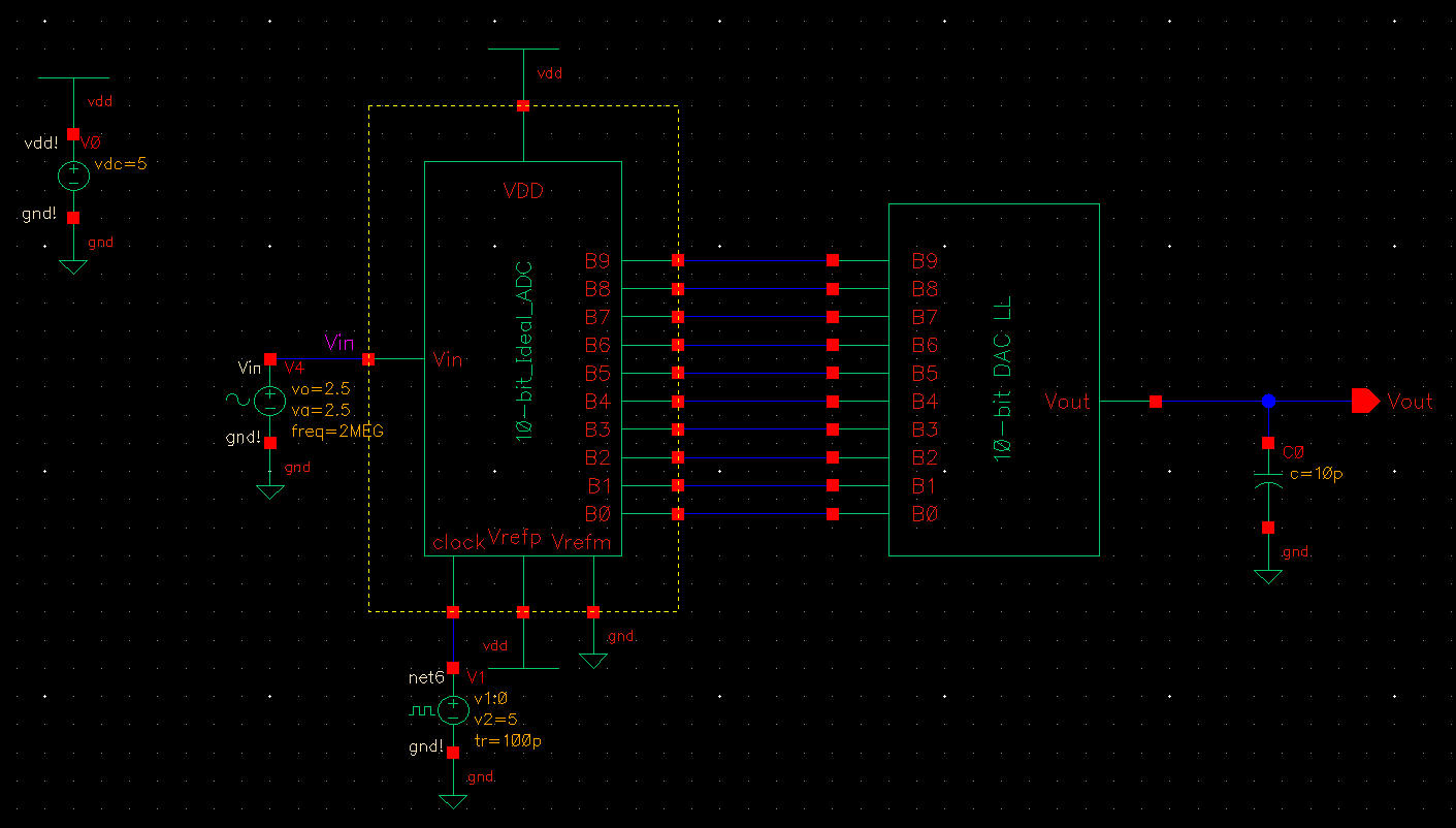
Figure 4: showing the schematic view of the DAC/ADC
Upon
completion of the simulation some experimentation was performed with
adjusting colors, proprtions and such of the graph display.
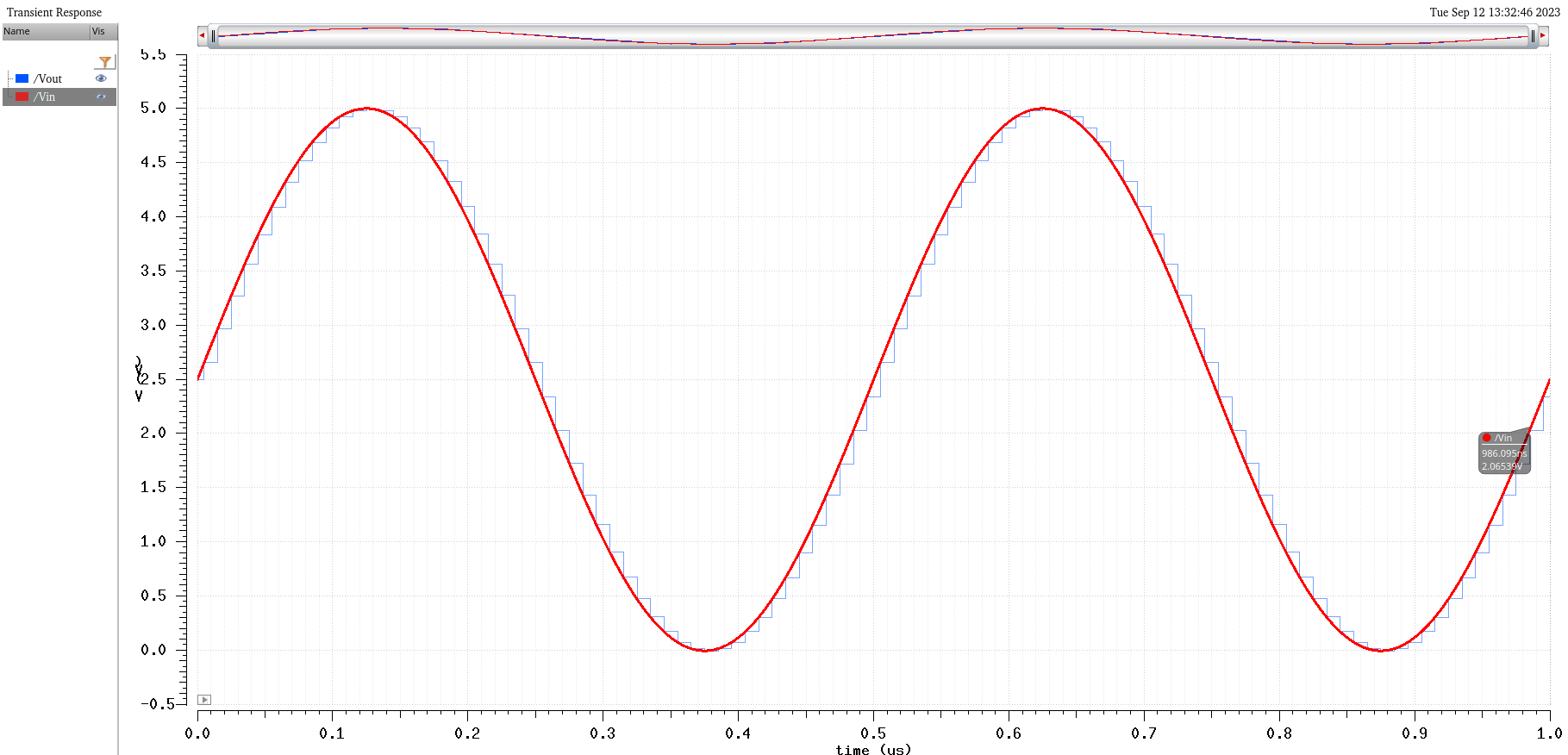
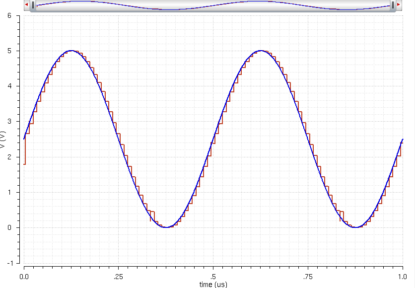
Figure 5: showing simulation results using the provided spectre simulation
From the simulation above we can see that the output bits B[9:0] change incrementally with an increase or decrease of the analog input signal.
Voltage Change Simulation to Test Functionality
To better determine the waveform incremental steps I will now run a simulation at a reduced voltage of 15mV amplitude with a 15mV offset to better observe the height of each step. This will reduce the number of steps as shown in the previous simulations above and provide a more detailed view.
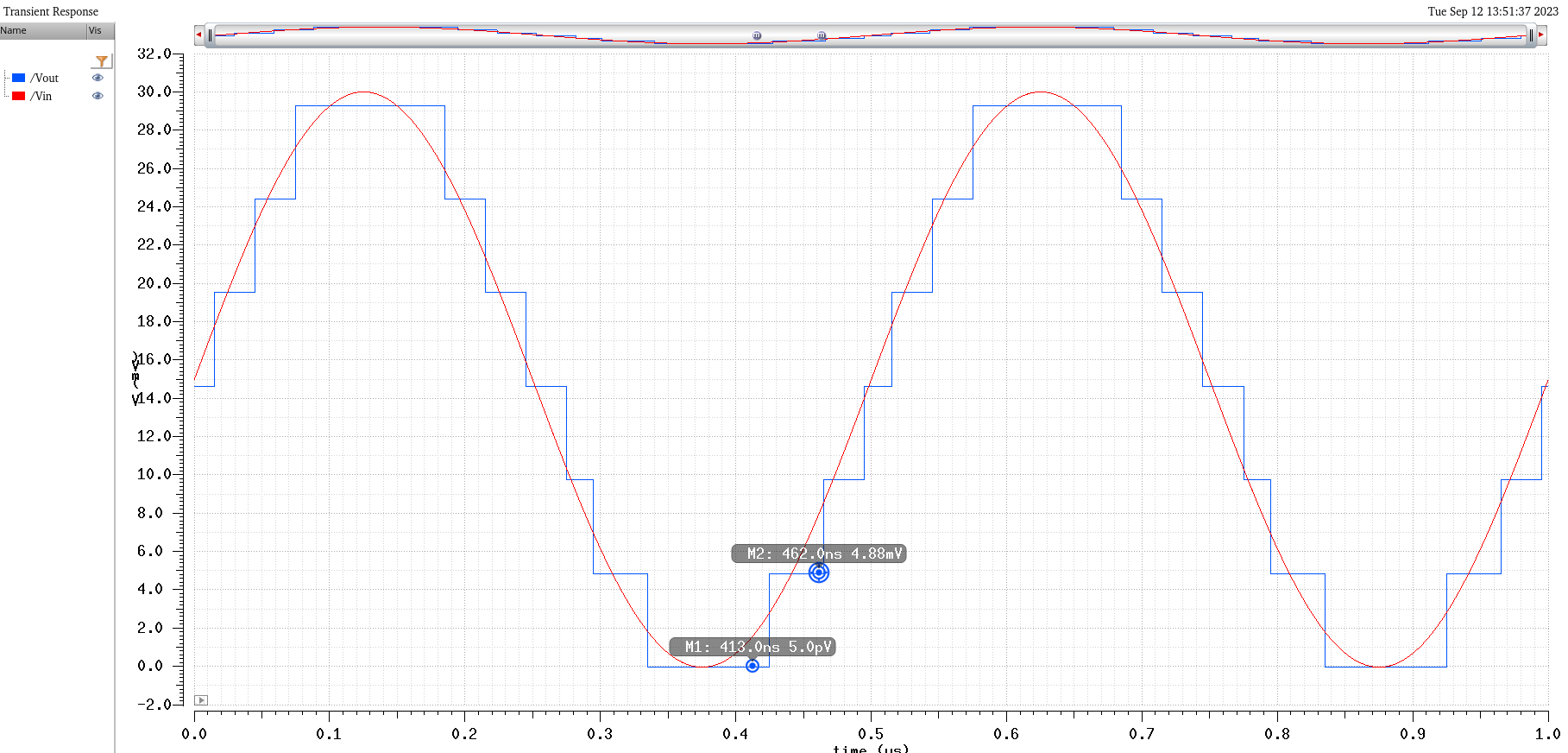
Figure 6: 15mV simulation to show steps in more detail
After completing the simulation, markers are placed at locations of the bottom and top of first step as this first step from zero level determines the least significant bit and represents the minimum change of the ADC that is required to influence a change in output bits B[9:0]. The voltage witnessed with a change of the LSB is 4.88 mV.
LSB (Least Significant Bit) Determination
Using the provided formulas from figure 30.14 the least significant bit can now be determined. Using our ADC's 10 bit architecture and VDD voltage of 5V dc I perform the calculation below.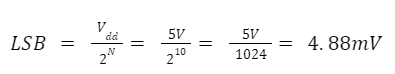
Equation 1: calculation of the minimum voltage for each step using 5V VDD voltage
Going back to reference our original VDD voltage of 5V we can now determine that the minimum voltage required to influence a single output bit change of B[9:0] is 4.88mV and this corresponds directly with the 15mV simulation results so the results align correctly as expected.
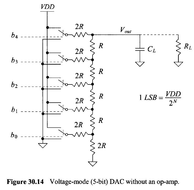
Figure 7: R - 2R Topology Example
Using 3 10k resistors I will first build the single bit voltage divider circuit which will then be turned into symbol and replicated 10 times to create a cascaded 10-bit digital to analog converter. Show below is the single bit circuit using 10k resistors using R - 2R topology.
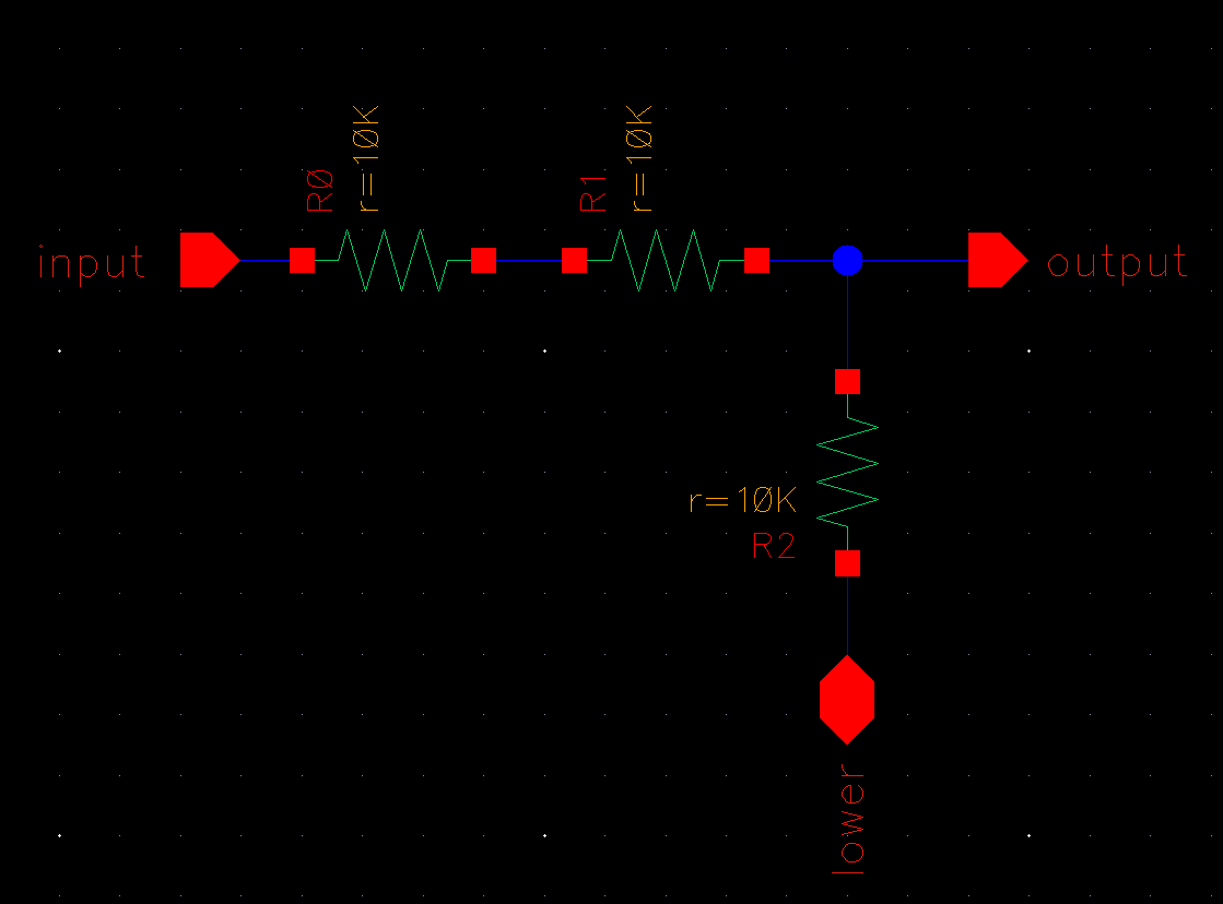
Figure 8: R - 2R Schematic Design for a Single Bit
The circuit above is then turned into a symbol by navigating to the create tab, click create cellview, then from cellview. Shown below is the created individual bit symbol that will now be cascaded to build the 10-bit DAC.
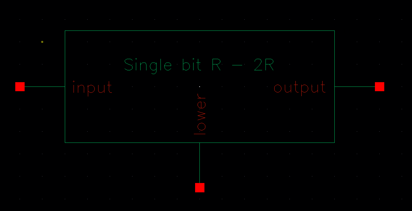
Figure 9: Single Bit DAC Symbol
Cascading
these will create the desired 10-bit circuit shown below. Once this is
completed a symbol will be created using the provided footprint in the
lab2.zip file and simulations can begin to test the circuit.
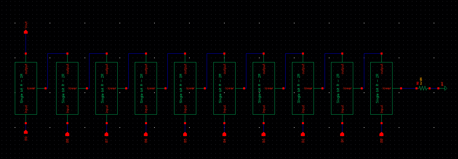
Figure 10: 10-bit DAC Schematic using cascaded single bit symbols
Using the same method decribed earlier for creating a single bit symbol from the schematic, a symbol view is created and shown below
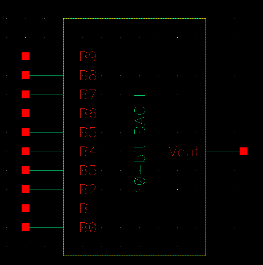
Figure 11: 10-bit DAC Symbol
The output reisistance will now be calculating at the Vout node to give us an overall equivalent resistance. The output resistance is found to be R or 10k in this design. Hand calculations are shown below.
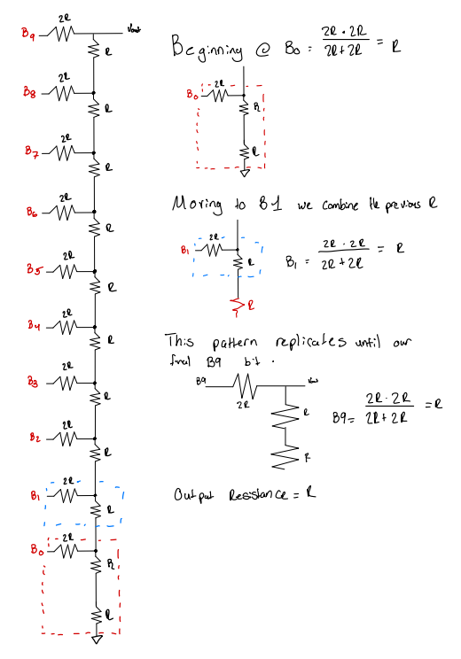
Figure 12: Equivalent Resitance Hand Calculations
Using the assumed R or 10K value to drive a capacitive load of 10pF, the time delay can now be calculated. Hand calculations are shown below.
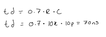
Figure 13: Time Delay Hand Calculations
Using a transient simulation with B[8:0] grounded and a DC pulse voltage applied to B[9], the delay will now be verified. Below we can see the circuit used and simulation results marked at 50% output prving the hand calucations to be correct.
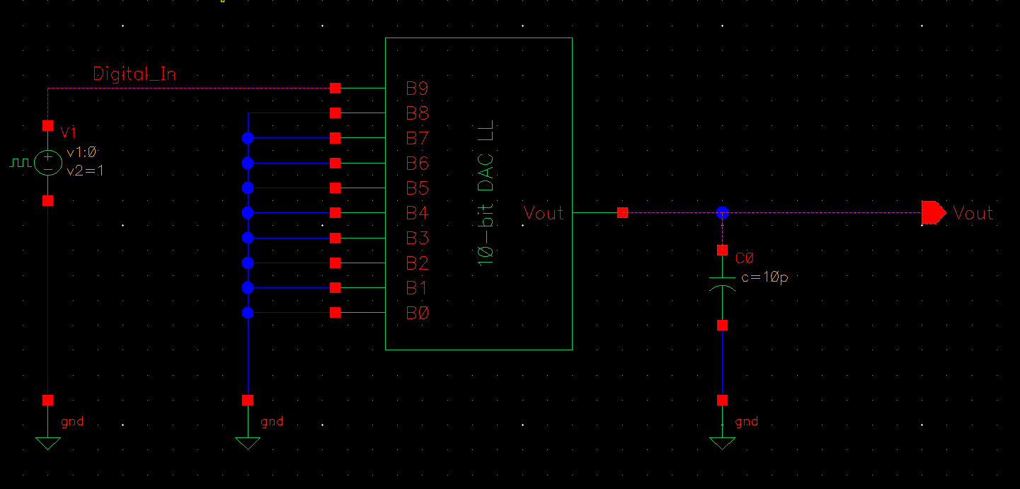
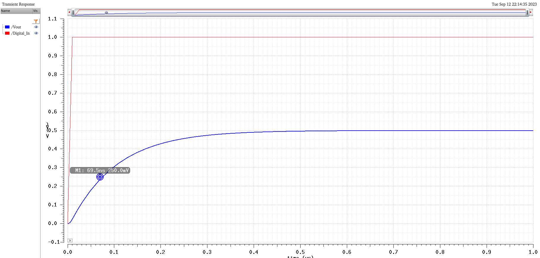
Simulation #1: Schematic and results showing DAC driving 10pF capactive load
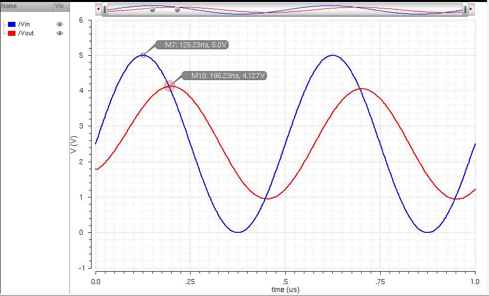
No Load Test of DAC
To
verify proper functionality of my design, the circuit will now be
simulated without a load and compared to that of the ideal DAC circuit
provided. Simulation schematic and output can be seen below.
Simulation #2: Schematic and results of no load DAC test simulation
We can see the above output provides a similar step to that shown in the ideal DAC provided.
10pF Load Test of DAC
The DAC will now be simulated using a 10pF load to test predicted output hand calculations. Schematic and simulation results can be seen below.
Simulation #3: Schematic and results of DAC using 10pF load
Analyzing
the output results shown above we can see again that the ouput lags the
input by approximately 70ns as expected by hand calculations.
RC load test of DAC
The
final simulation will involve the DAC driving a 10K resistor and 10pF
capacitor. Simulations results and schematic are provided below.
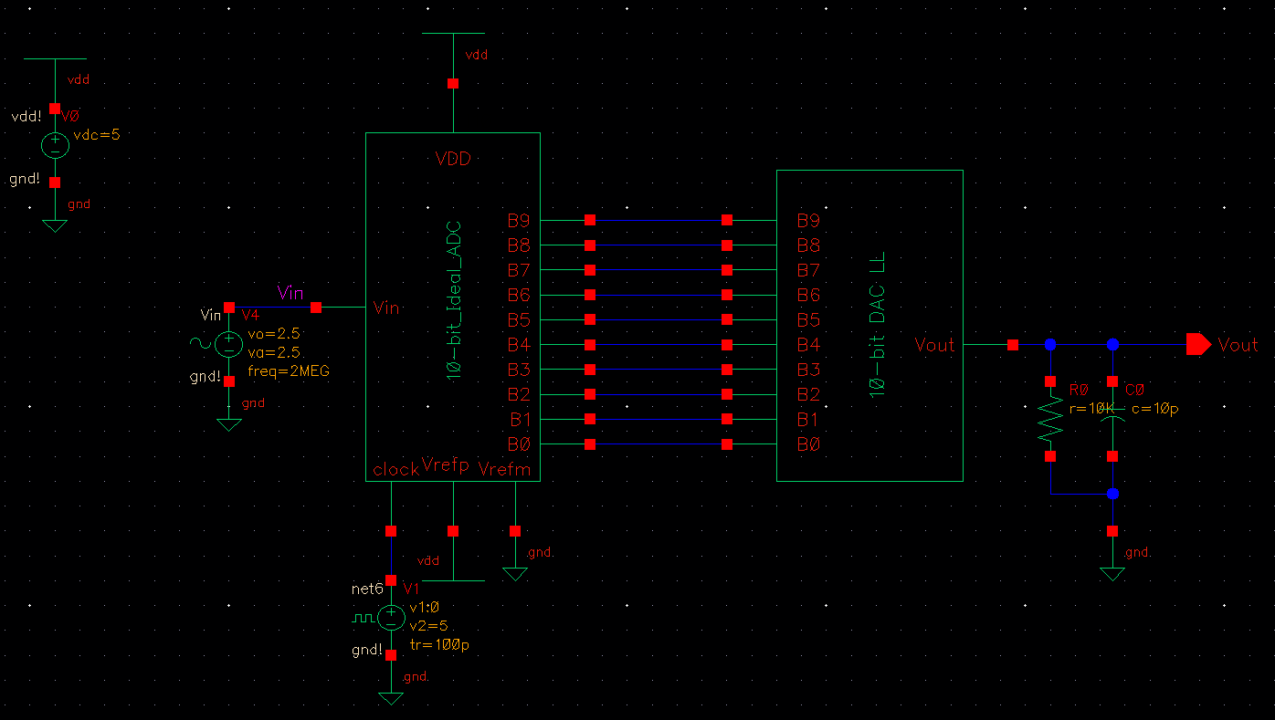
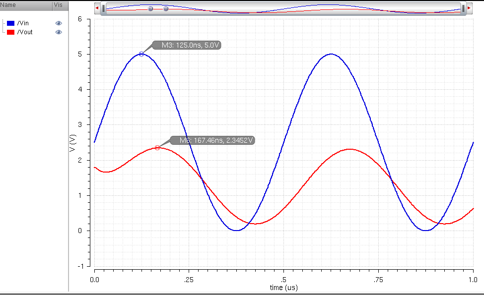
Simulation #4: Schematic and results of DAC driving 10K resitor and 10pF capacitor in parallel
Viewing the simulation results above we can see the Vout is half the input while also lagging by approximently 40ns
Problem Encountered:
I had some trouble with convergence during the simulations shown above and had to modify values within the analog simulator settings to force an output. These values can be seen below and can be edited in the ADE through Simulations -> Options -> Analog. This did not always work even if the values were changed repeated times. I need to look further into this as it might be a problem down the line. My only clue is with one of the given components was sighted an option saying "blowup" range needs to be changed beyond 1.5GA
Conclusion
After
reviewing all simuation results in comparison to the provided ideal
10-bit DAC model, I can confirm this design functions as expected and
performs properly as a digtial to analog converison device. When
reviewing the simulations without a capacitive load our output remains
in phase with the input even when a resitive load is applied. However,
when applying a capacitive lone a significant output phase lag is
witnessed which can be reduced with the addition of a resistor in
parallel to the capacitor.
Post Lab Questions
Discuss
what happens when the resitance of the switches in the outputs of the
ADC (modeled as ideal) are not not small compared to R:
Having
a significant switch resistance relative to R would impact overall
equivalent resistance for the device and significantly impact output
results and overall functionality. Each switch resistance would be need
to be calculated individually and it's respective resistor values would
need to be modified individually to optimize the device's funtionality.