Lab 7 -
EE 421L
Authored
by Josh Jensen
jensej3@unlv.nevada.edu
10/25/23
Lab 7: Using buses and arrays in the design of word inverters, muxes, and high-speed adders
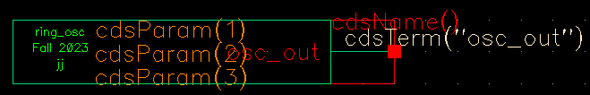
Prelab: Go through Tutorial 5
This tutorial walked through the steps of building a ring oscillator schematic, symbol, and layout
from basic components (such as the inverter).
Schematic:
Symbol:
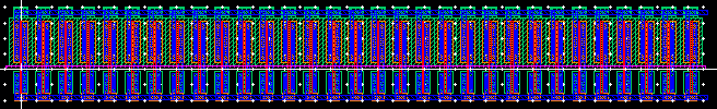
Layout: (click for a larger picture)
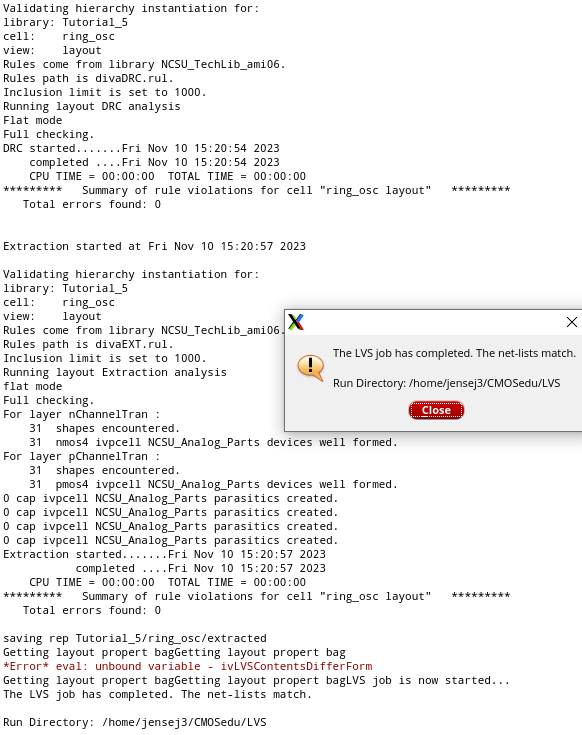
Last but not least, the design rule verification:
Lab:
First, I followed the outlined process of simulating the 4-bit inverter array.
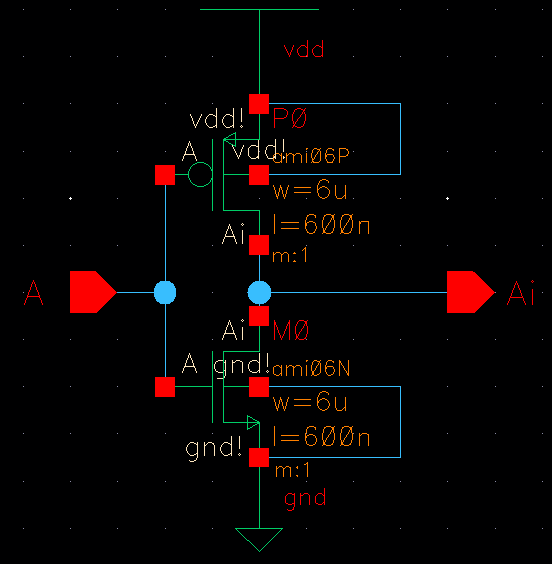
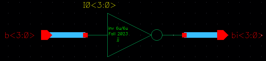
Inverter schematic:
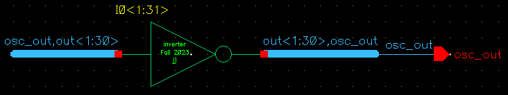
4-bit inverter array, using the inverter symbol:
Simulation schematic for the 4-bit inverter array:
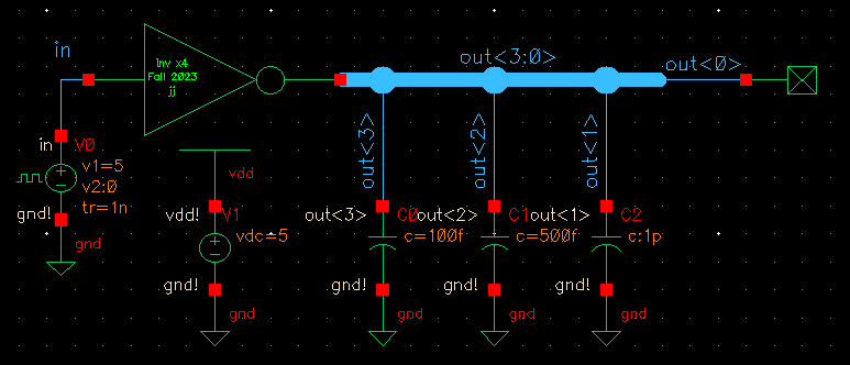
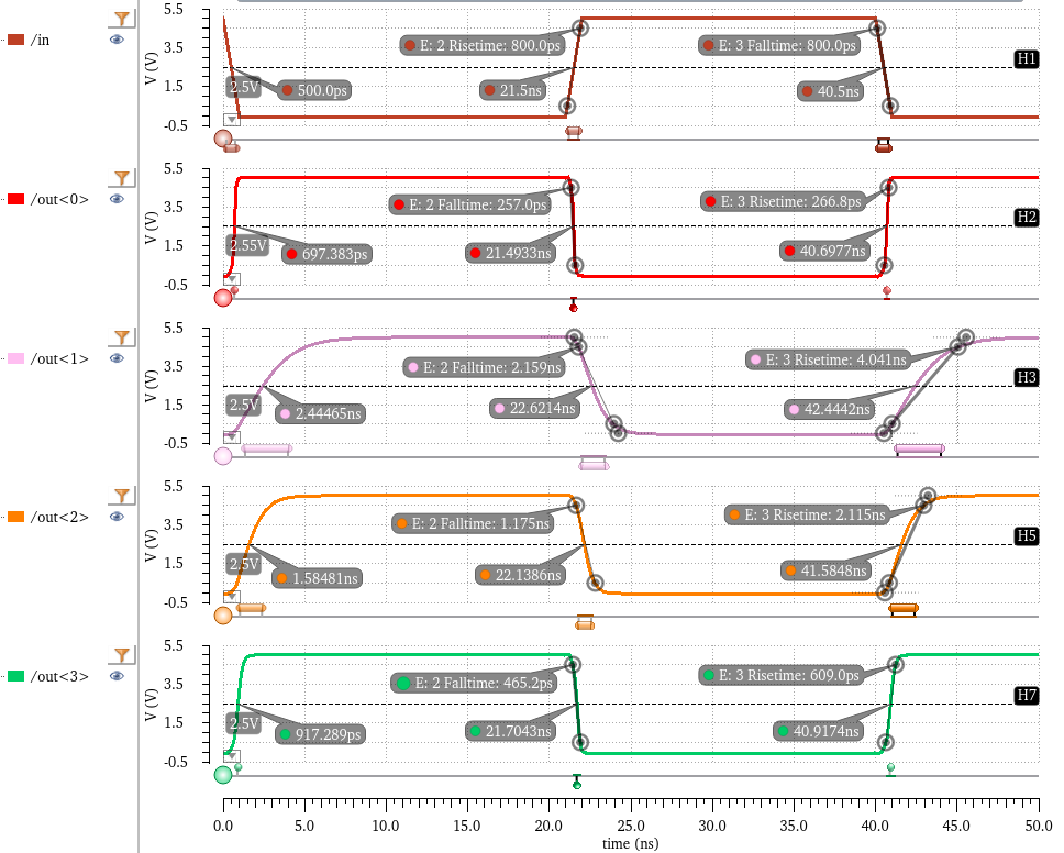
Results for this simulation:
The effects of the capacitive loads are seen in the delays as well as the rise and fall times of the signals.
*For the following measurements, I used a 10%-90% definition for rise and fall times.
We
see that without any capacitor, out<0> has barely any delay, and
in the middle of this section even appears to cross the 2.5V
midpoint
before the input signal (21.4956ns vs 21.5ns). The rise/fall times are
also rather small at less than 50ps each. However,
the
fall time is noted to be about half that of the rise time. This is
because the transistors used are all 6u/0.6u, so the PMOSes
have less resistance (by about half) than the NMOSes. As rise time is proportional to the PMOS resistance and fall time is
proportional
to the NMOS resistance, this leads to the rise time being about half of
the fall time. This general trend will continue
for
the rest of the inverter signals and probably for the rest of the lab
as well, because the transistors will remain the same size.
This doubling can also be seen in the delays for rising signals vs falling signals, for the same reason.
Comparing
this to the out<3> signal, which runs through a relatively weak
100fF capacitor, we see increased delays of about 400ns
(rise) and 200 ns (fall), as well as increased rise times (about 600ps) and fall times (about 470ps).
Now
looking at the heaviest capacitor in this simulation, out<1> has
to run through a much larger 1pF capcitor. This is reflected in
delays
of 1.1ns (rise) and 1.9ns (fall) as well as edge transitiions of 4ns
(rise) and 2.2ns (fall), which are again much larger than those
of out<3> or out<0>.
Next, I moved on to making 8-bit versions of NOT, NAND, NOR, AND, and OR gates.
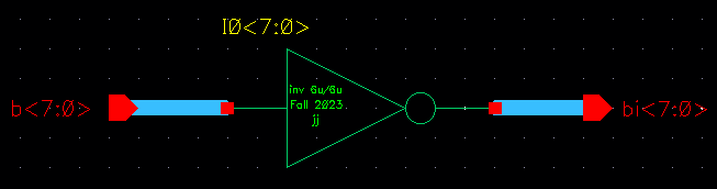
8-bit inverter schematic:
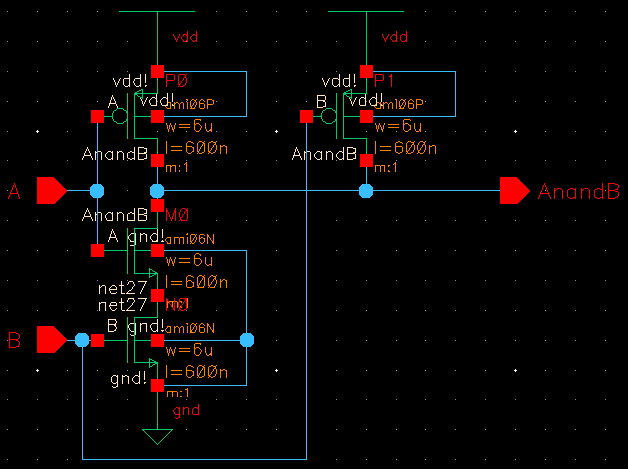
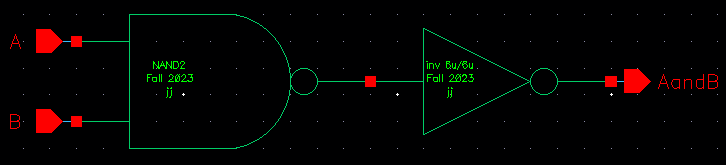
1-bit NAND gate schematic:
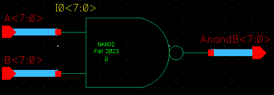
8-bit NAND schematic, using the 1-bit NAND symbol:
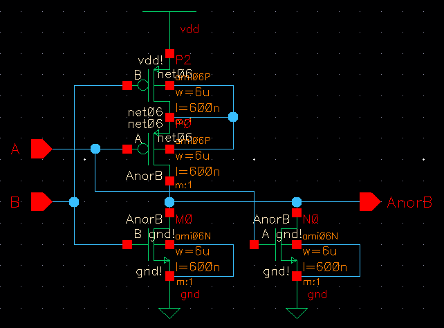
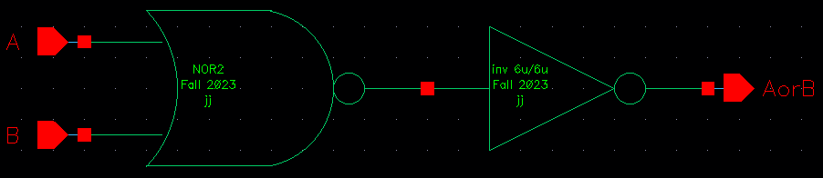
1-bit NOR schematic:
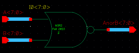
8-bit NOR schematic, using the 1-bit NOR symbol:
To make the AND and OR gates, I simplified my work by reusing the NAND, NOR, and NOT symbols.
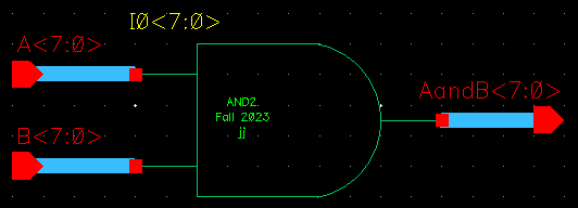
1-bit AND schematic, using the NAND and NOT symbols:
8-bit AND schematic, using the 1-bit AND symbol:
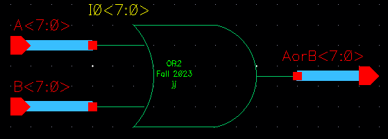
1-bit OR schematic, using the NOR and NOT symbols:
8-bit OR schematic, using the 1-bit OR symbol:
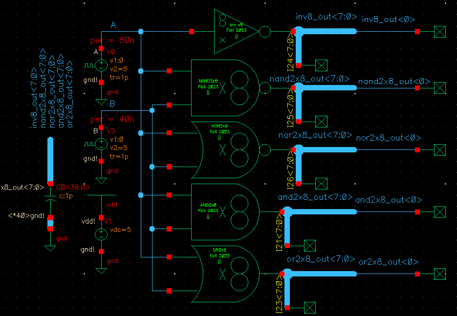
Next, I simulated the 8-bit NOT, NAND, NOR, AND, and OR gates all together.
I went ahead and used a 1p capacitor per output signal to mitigate signal spikes (it was rather extreme for the NOR gate in
particular). I only plotted one output bit from each gate since all 8 bits in each set would be the same anyway.
Gate simulation schematic:
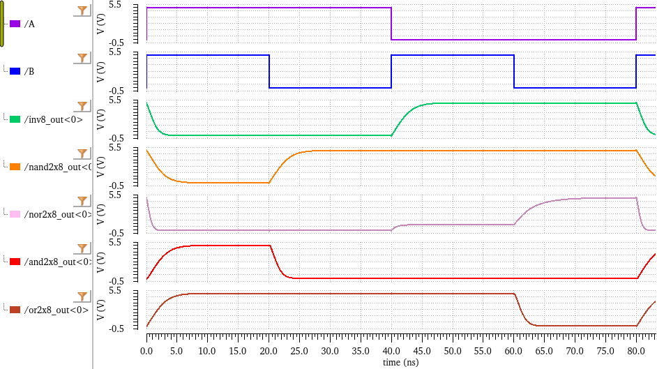
Gate simulation results:
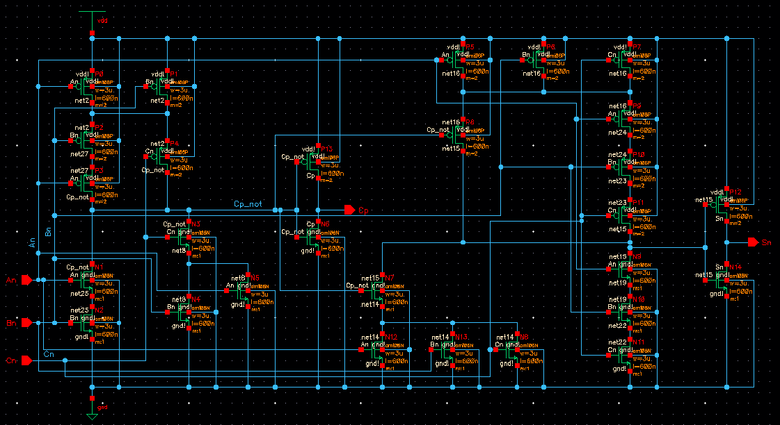
Next, I created an 8-bit full adder using the AOI design from Figure 12.20 in the textbook. For reference...
Schematic: (click image for a larger version)
As this is a new schematic I wasn't entirely familiar with, I decided to simulate it just to make sure it worked as expected.
Simulation schematic:
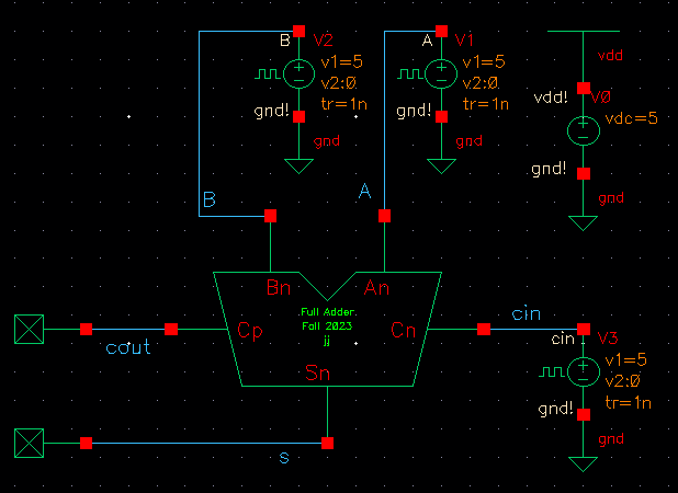
Simulation results:
Yes, this works correctly.
0+0+1 gives a carry out of 0 and a sum of 1 (01).
0+1+1 gives a carry out of 1 and a sum of 0 (10).
1+1+1 gives a carry out of 1 and a sum of 1 (11).
After
confirming that it worked, I made the layout for a single-cell full
adder. The inputs and outputs are on the metal 2 layer.
Layout:
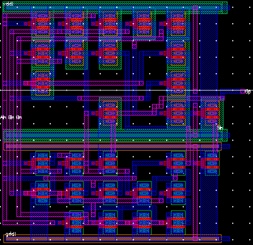
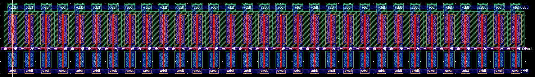
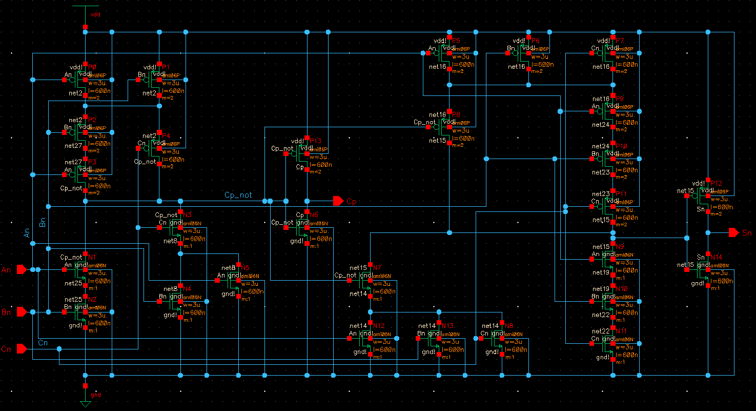
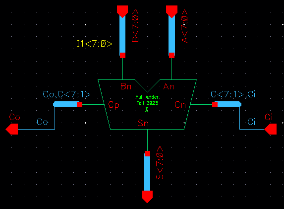
Next, I made an 8-bit version of the full adder.
Schematic:
I used Ci to represent the initial carry in, Cp to represent Cn+1, and Co for the final carry out.
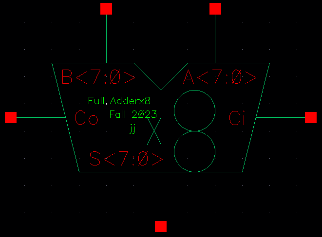
Symbol:
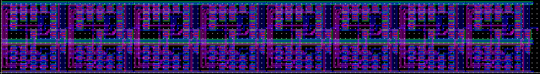
Layout: (click for a larger version)
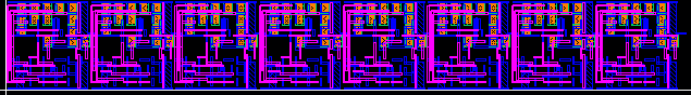
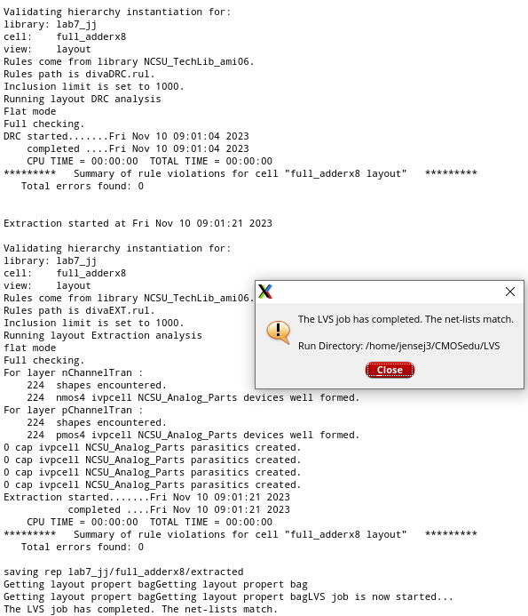
Design rule checks:
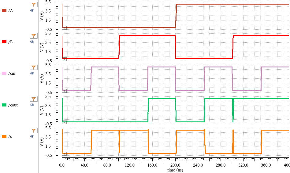
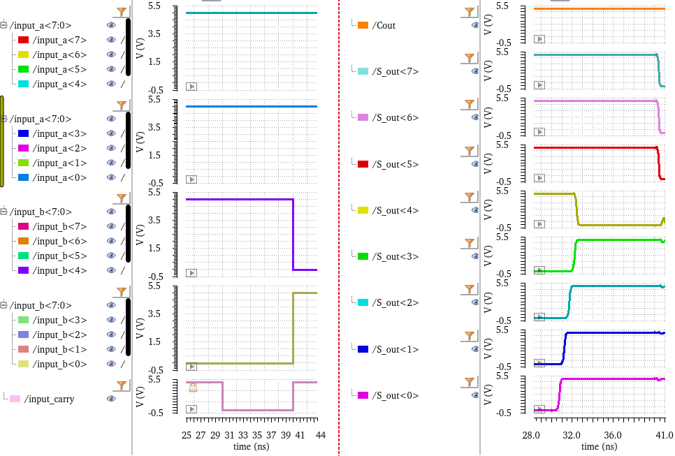
To simulate the 8-bit adder, instead of simulating all possible 2^17-1 input combinations,
I just varied A<7:4>, A<3:0>, B<7:4>, B<3:0>, and Ci as if it were any other 5-variable
logic function.
For
example, at 36 ns, A = 1111 1111, B = 1111 0000, and Cin = 0. I would
expect that the lower four bits of A would stay intact,
while the upper four bits of A and B would sum to produce 1110 and an overflow to carry out.
We see that this is what happens, as S = 1110 1111 and Cout = 1 at 36 ns.
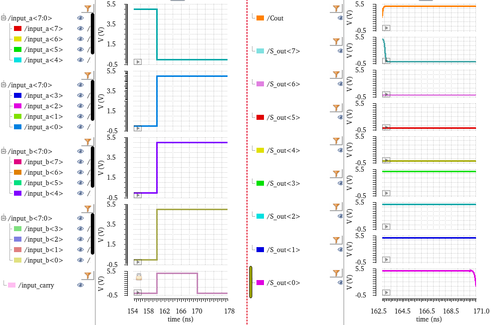
For
another example, here is the plot at 166 ns. At this point, A = 0000
1111, B = 1111 1111, and Ci = 1. Performing the binary addition
by hand, I would add Ci to B, which would reset B to 0000 0000 and sending the overflow 1 to Cout. After that, A + 0000 0000 is
simply A, or 0000 1111. This is reflected in the graph, as we see S<7:4> is 0000, S<3:0> is 1111, and Cout = 1.
Instruction
for Lab 7
Return
to list of my EE421L labs