
Lab 6 - EE 421L
Prelab: Go through Tutorial 4
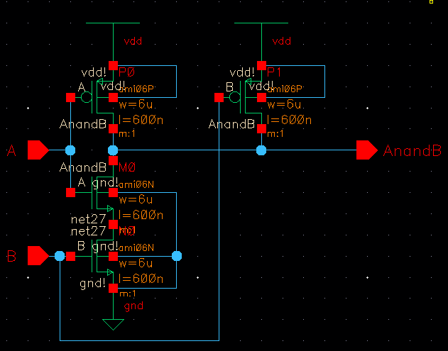
I followed Tutorial 4 to create a 2-input NAND gate, first using a PMOS sizes of 12u/0.6u
and NMOS sizes of 6u/0.6u. This is intended to conflict with the schematic, which uses PMOS
sizes of 6u/0.6u.
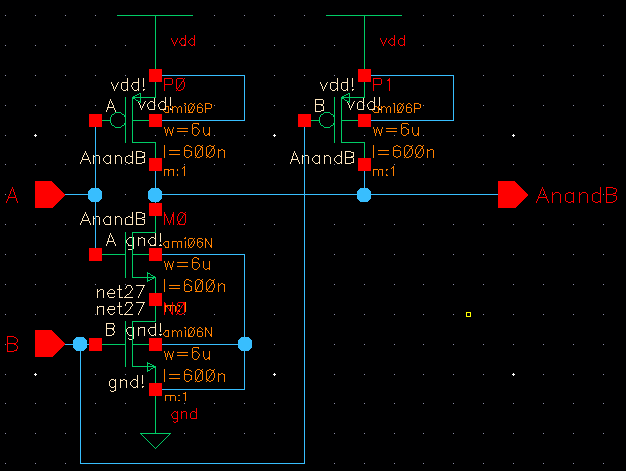
This is the schematic, showing the 6u/0.6u PMOS devices:
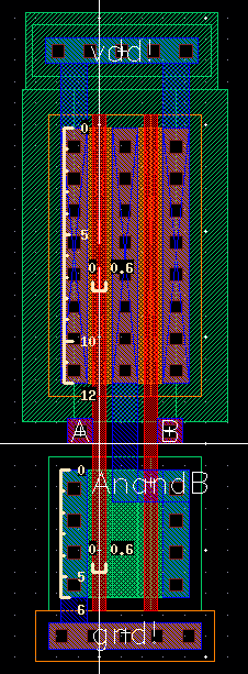
Here is the first layout of the NAND gate. Note how the PMOS widths are 12u.
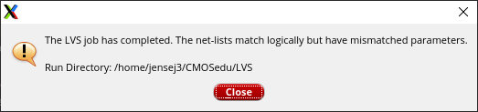
I used the LVS option "Compare FET Parameters" to intentionally fail because of mismatched sizes:
I then fixed the layout, so the parameters would match. Note that the PMOS widths are now 6u.
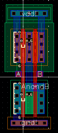
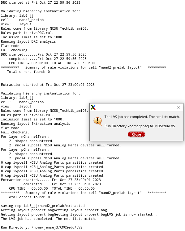
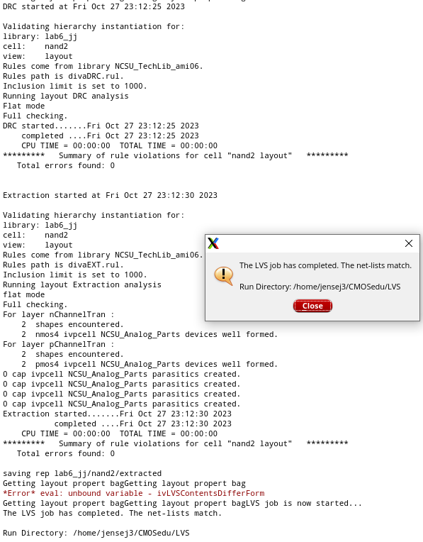
These are the successful DRC, Extraction, and LVS checks for this layout.
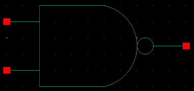
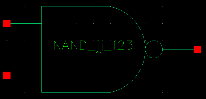
Finally, I practiced making a NAND gate symbol for use in simulations.
Lab:
First, I used my work from the prelab to create the NAND gate schematic, layout, and symbol.
I labelled the symbol as per the lab instruction, with the type of gate, my initials, and the semester.
Clean DRC, Extraction and LVS results for the NAND gate:
I simulated both the NAND gate and XOR gate together, so I will show those results later.
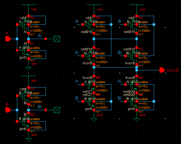
Next, I made an XOR gate using PMOS sizes of 6u/0.6u and NMOS sizes of 6u/0.6u as well.
This design first uses two inverters to obtain the complements of inputs A and B, then uses several
pathways to implement the desired output behavior. The two pairs of series NMOS ensure that if
both A and B are equal, the output is pulled down to ground. Likewise, if A and B are equal, then there will be
one row of PMOS that is off and preventing VDD from reaching the output. It is only if A and B differ that
there will be a path from VDD to output AxorB.
Here is the schematic:
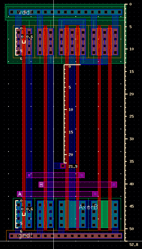
Here is the layout I implemented. I used the metal2 layer to connect across the lines of metal1 or
poly1 as necessary, but all inputs and outputs are still on the metal1 layer. It was at this point that
I realized I should probably use a larger standard cell size in order to accomodate the later full
adder layout and the extra signals that it would have. I figured that since the full adder would have
7 total signals, planning for 10 signals' worth of extra space would be sufficient. I calculated the
space required using the logic of 0.9u spacing between metal layers and 1.2u width of the metal layers,
so 2.1u per signal with an extra 0.9u on the far side. This evaluates out to 2.1u * 10 + 0.9u = 21.9u.
With this in mind, I made this layout with 21.9u of extra space and measured the total width of the
layout so I could modify the earlier NAND design to also conform to the standard cell size.
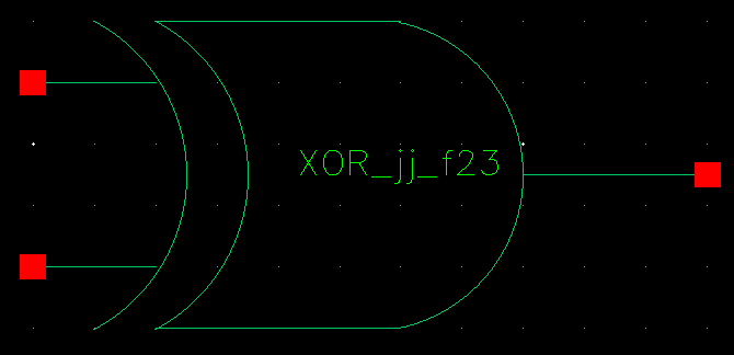
Here is the symbol for the XOR design:
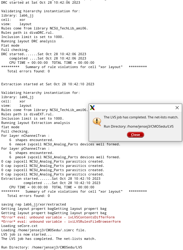
And here are all of the successful design rule checks:
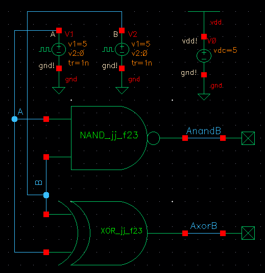
At this point, I ran simulations to confirm that the NAND and XOR gates function as desired.
In this schematic, the A voltage source alternates every 200ns and the B voltage source
alternates every 100ns, so in 400ns I expect to see every combination of A and B logic values.
Finally, here is the simulation. Please click the image to see it in full resolution.
First, A (blue) and B (red) alternate as desired, with values of 00, 01, 10, and 11
occuring at 0, 50, 100, and 150 ns respectively.
Second, AnandB (green) is active for all AB logic values except for 11, as expected
of a NAND gate.
Third, AxorB (purple) is active for logic values 01 and 10, and is low for 00 and 11.
This confirms that both the NAND and XOR gates are working correctly.

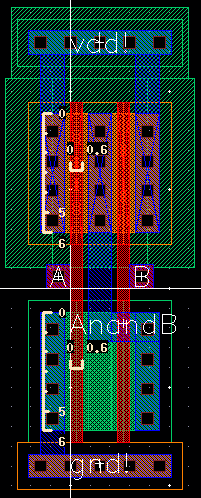
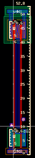
Next, I modified the earlier NAND layout to fit within the same standard cell as the XOR gate.
It is a little cluttered but note that the total width of the layout is the same 52.8u as the XOR.
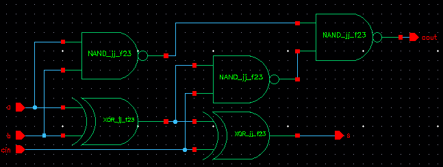
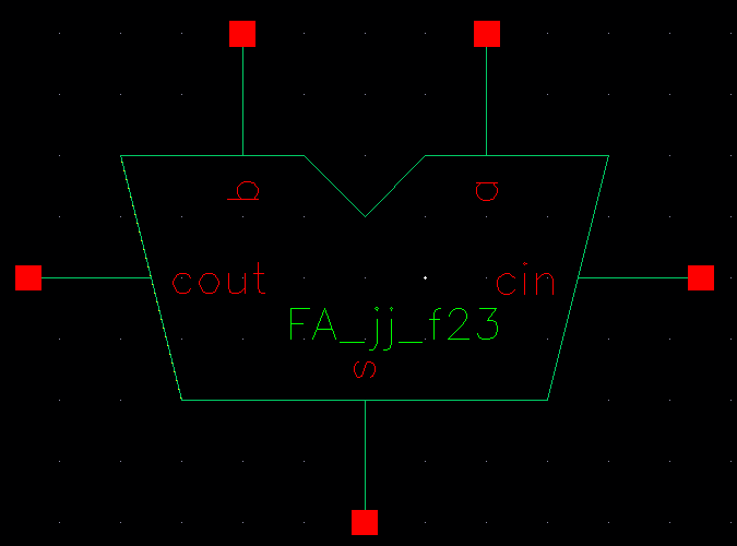
Next, I started on the full adder. Here are the associated schematic and symbol:
Here is the layout I made to implement this design, using the standard cell NAND and XOR gates.
The input pins a, b, and cin as well as the output pins s and cout are all on the metal2 layer. Please
click the image to view the layout with more zoom.

Here are the associated design rule checks for this design:

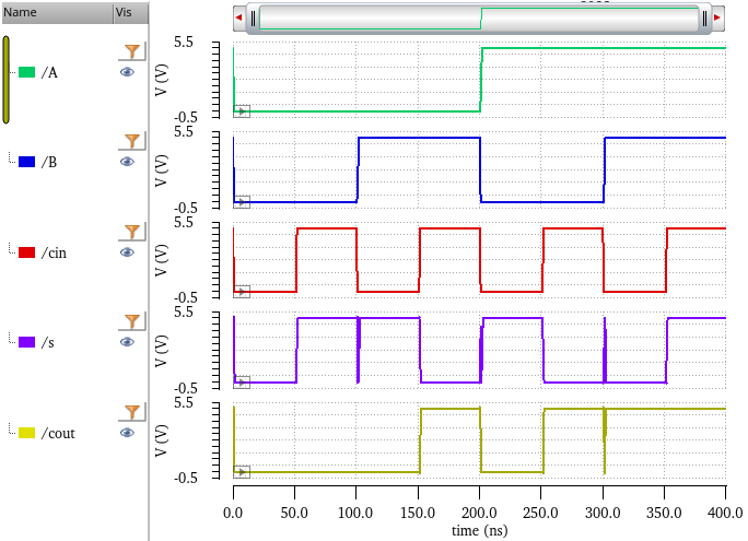
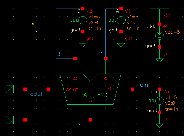
Last but not least, I simulated the full adder to confirm it works correctly for all values
of a, b, and cin. This is organized similarly to the NAND and XOR simulation, with A
and B alernating at periods 400ns and 200ns, only now with cin alternating with a period
of 100ns. This means that the simulation will test a new logic case every 50ns, covering
all 8 possible combinations over the total 400ns.
Here are the resulting simulation plots. I will break down the results and compare them to the
expected values for each time section. As you can see, the simulation results confirm that the
full adder device is functioning as desired.
| Time (ns) | a | b | cin | Obtained | Expected | Valid | ||
| s | cout | s | cout | |||||
| 0 | 0 | 0 | 0 | 0 | 0 | 0 | 0 | Yes |
| 50 | 0 | 0 | 1 | 1 | 0 | 1 | 0 | Yes |
| 100 | 0 | 1 | 0 | 1 | 0 | 1 | 0 | Yes |
| 150 | 0 | 1 | 1 | 0 | 1 | 0 | 1 | Yes |
| 200 | 1 | 0 | 0 | 1 | 0 | 1 | 0 | Yes |
| 250 | 1 | 0 | 1 | 0 | 1 | 0 | 1 | Yes |
| 300 | 1 | 1 | 0 | 0 | 1 | 0 | 1 | Yes |
| 350 | 1 | 1 | 1 | 1 | 1 | 1 | 1 | Yes |