Lab 5 -
EE 421L
Authored
by Josh Jensen
jensej3@unlv.nevada.edu
9/27/23
Lab 5: Design, layout, and simulation of a CMOS inverter
Prelab: Go through Tutorial 3
Here are the results of the inverter I created, following the tutorial.
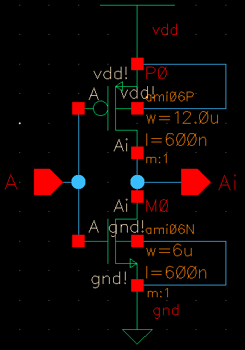
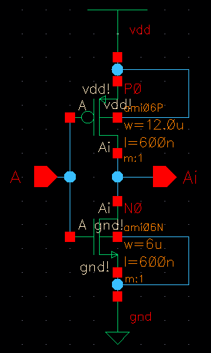
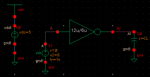
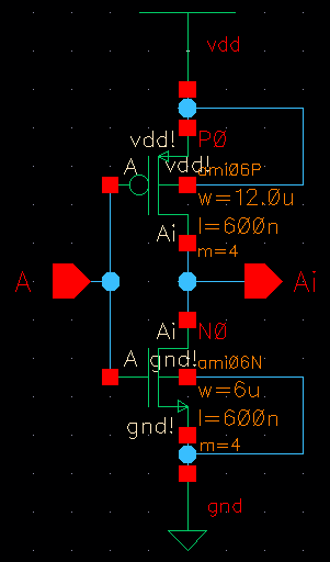
Inverter schematic:
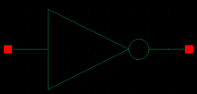
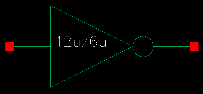
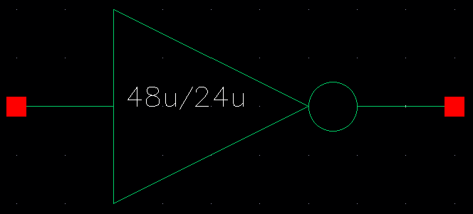
Inverter symbol:
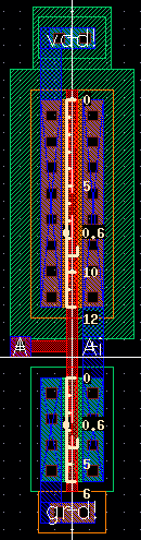
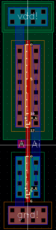
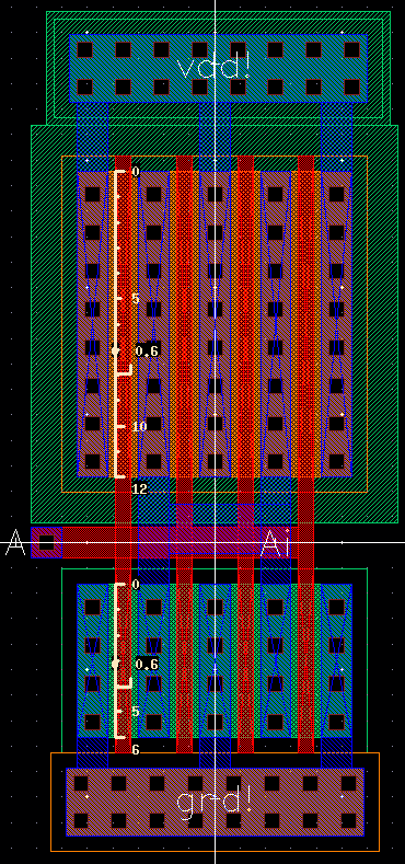
Inverter layout:
Please note the measured 12u/0.6u dimensions of the PMOS as well as the 6u/0.6u NMOS.
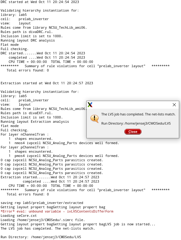
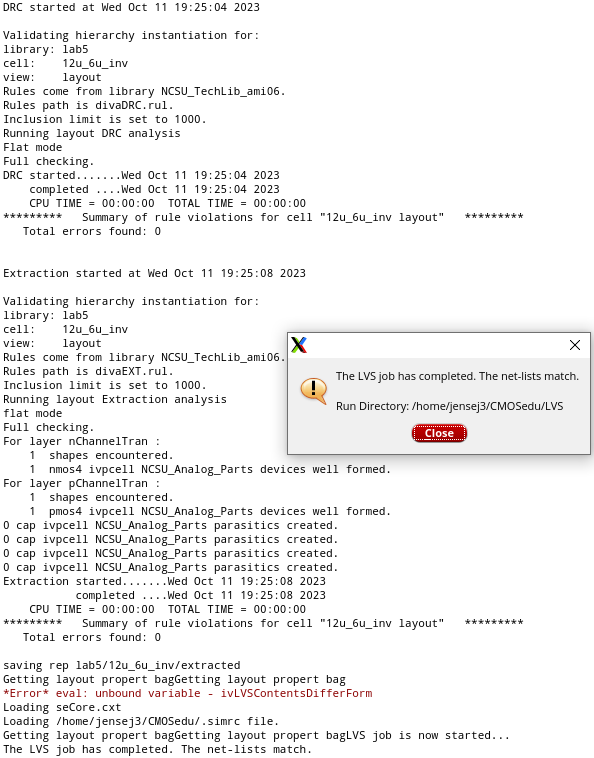
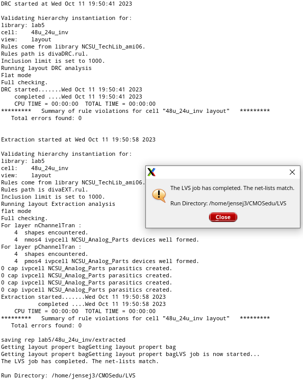
DRC/LVS pass:
Lab:
First, I made a 12u/0.6u PMOS, 6u/0.6u NMOS inverter. This was very similar to
the prelab work from Tutorial 3.
Schematic:
Symbol:
Layout:
As in the prelab layout, please note the measured dimensions for the PMOS and NMOS.
Two rows of contacts for the vdd and gnd rails help to reduce the equivalent resistance,
and there are more replacements available if ever there is a problem with some of the contacts.
DRC/LVS pass:
Next, I ran some simulations to judge how well this inverter drives capacitive loads.
This is important because in IC design we will often need to drive signals through
off-chip loads.
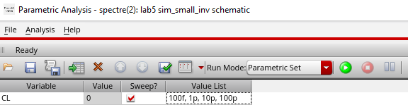
(100 fF, 1 pF, 10 pF, 100 pF loads):
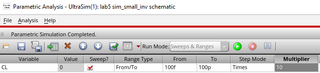
I used the same idea from lab 4 to run the same simulation multiple times for varying values of CL, using the
parametric analysis function. This time, I changed it slightly to allow me to directly enter the list of values.
ADE L:
Here we see that the inverter is able to drive a signal through the smallest capacitor here (100fF), but struggles
to do the same for higher capacitance loads. I used a marker at 2.5V (VDD/2) to judge the delay for each case.
At 100fF the delay is minor at about 0.26ns, but it gets worse at 1.14ns (1pF) and almost 10ns (10pF).
Within the 5ns rise time and 10ns at VDD, the output signal barely falls below 2.5V and 4.75V for 10pF and
100pF loads, respectively.

Please click to enlarge the image.
Ultrasim:
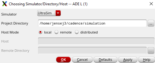
I needed to make some changes to the ADE window in order to run the Ultrasim simulation.
First, of course I needed to actually change the simulator setting from Spectre to Ultrasim.
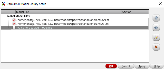
Next, I had to add the models for the NMOS and PMOS, as it didn't carry over the settings from Spectre.
Finally, I had to change the parametric analysis slightly as it was not allowing me to use a predefined list of values for CL.
The Ultrasim results are more accurate than the previous Spectre results, but they give similar conclusions.

Please click to enlarge the image.
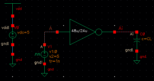
48u/0.6u PMOS, 24u/0.6u NMOS (both M4) inverter:
Schematic:
Symbol:
Layout:
Please note the measured 12u/0.6u PMOS dimensions as well as 6u/0.6u NMOS, both of which
have four fingers. This means that the PMOS is equivalent to 48u/0.6u and the NMOS 24u/0.6u.
DRC/LVS pass:
Simulations (100 fF, 1 pF, 10 pF, 100 pF loads):
ADE L:
Now that we are using an inverter which is four times the size as before (12u/6u to 48u/24u), we see that it
is better able to handle the same loads. Comparing to the previous results:
- For 100fF, we are down to about 0.15ns, from 0.26ns.
- For 1pF, we are down to about 0.43ns, from 1.14ns.
- For 10pF, we are down to about 2.6ns, from almost 10ns.
- For 100pF, we are still unable to drive the output down to 2.5V, but it is able to reach 3.9V (instead of 4.75).
These results clearly show increasing the size of the inverter is very effective in reducing the propagation delay
in driving a signal through a capacitive load off-chip.

Please click to enlarge the image.
Ultrasim:

Please click to enlarge the image.
Zipped lab directory:
lab5_jj.zip
Instruction
for Lab 5
Return
to list of my EE421L labs