todo: redo pmos/nmos layout far
Lab 4 - EE 421L
Prelab: Go through Tutorial 2
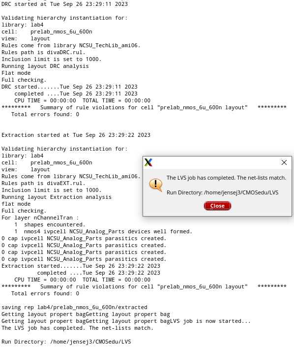
First, we were instructed to make an NMOS transistor with dimensions of
6um width and 6nm length.
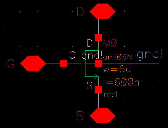
This is the schematic. Note that the body is tied to the gnd! net, as we want
the bulk of our NMOS devices to be tied to ground.
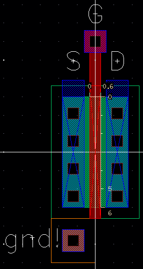
This is the layout of the device. I've placed rulers to show that the correct
dimensions were used, and how they are measured on the transistor.
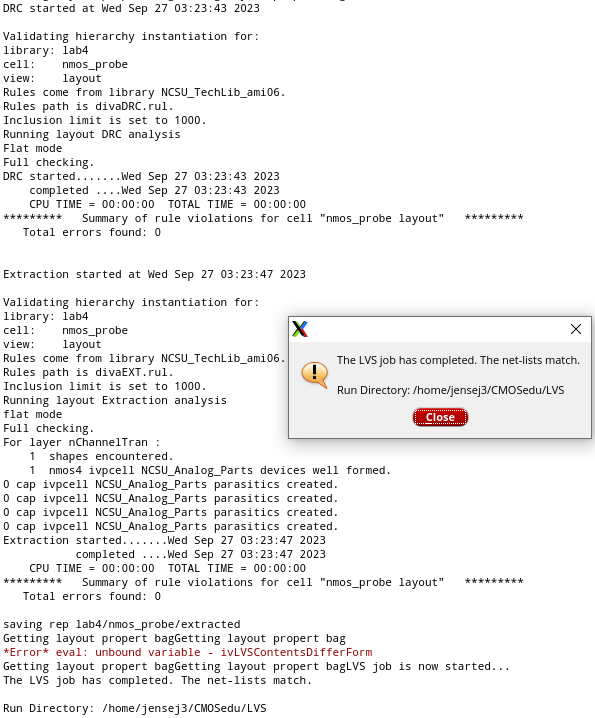
Next, I ran my DRC, Extraction, and LVS checks to make sure this design was good.
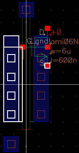
To verify one more time, we can look at the extracted view to see that the
software recognized the device I wanted to implement.
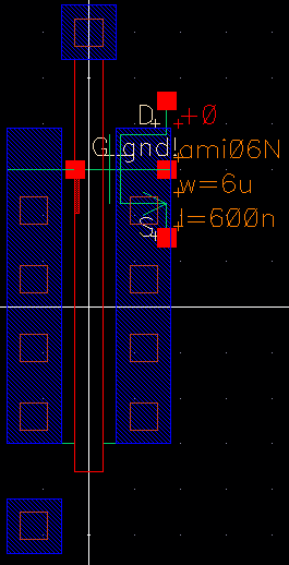
If we click on either the nodes of the schematic shown here or the metal/poly
layers shown in the background, the corresponding element is highlighted. For
example, I can click on the top left portion of metal1 to highlight the S node
in the schematic, or vice-versa. This confirms that that piece of metal1 was
indeed interpreted as the source node of the transistor.
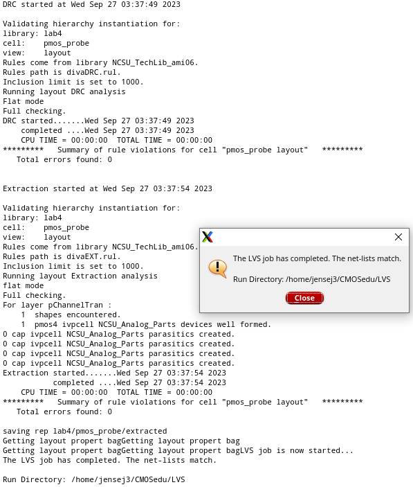
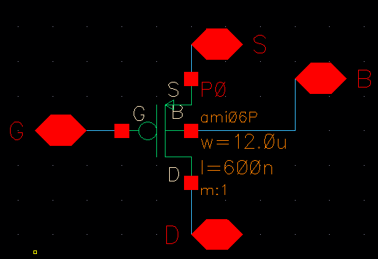
Next, we followed the tutorial to create a PMOS. The given dimensions were
12um by 600nm, and this time, we were to connect a B pin to the body instead
of tying it to a net. Here is the schematic.
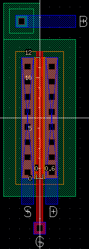
Next up is the layout, with dimensions shown.
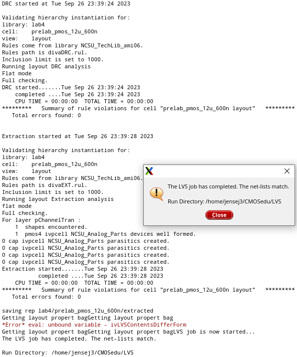
Here are the DRC, Extraction, and LVS checks, all passed.
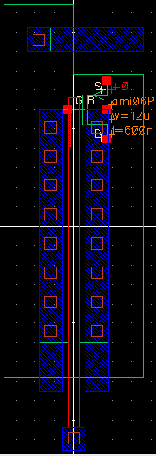
And as before, here is the extracted view.
Lab:
First, we ran some simulations. The NMOS devices are 6u/0.6u and the
PMOS devices are 12u/0.6u.
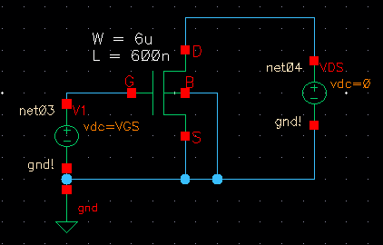
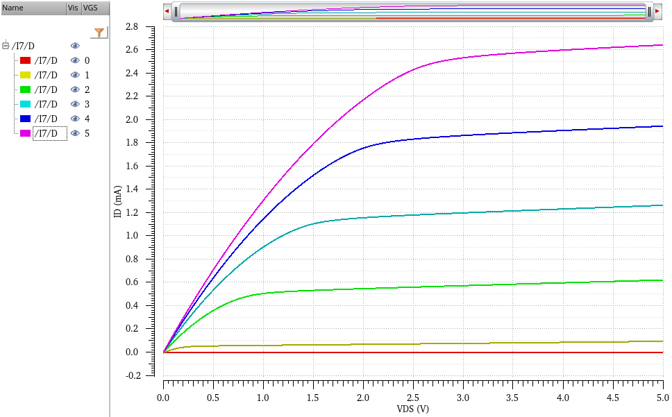
Simulation 1: I_D vs. V_DS of an NMOS.
V_GS will be tested from 0 to 5V in steps of 1V
V_DS will be tested from 0 to 5V in steps of 1mV
Here is the pertinent schematic.
For this first simulation, I'll briefly summarize the steps of setting up
the simulation.
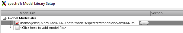
First, we need to make sure we include the models for the transistors we are
using. In this simulation we are only using an NMOS, so we include that model.
Next, we set the V_GS to 0V in the design variables. This is just an arbitrary
value for now and will be changed in the parametric analysis window. The dc
analysis here allows us to do the 0-5V variation of V_DS.
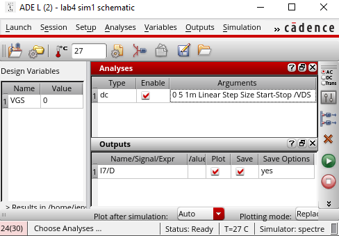
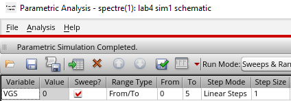
Next, we set up the parametric analysis to allow us to plot separate curves
for each of the V_GS values (0, 1, 2, 3, 4, and 5V).
Finally, here are the resulting I-V curves.
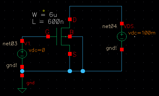
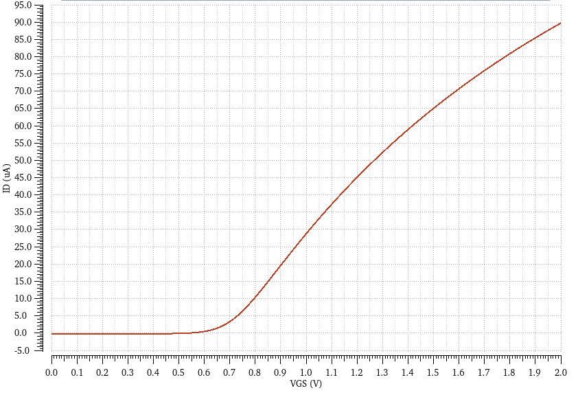
Simulation 2: I_D vs. V_GS of an NMOS. This is the same as simulation 1,
but V_DS will be kept constant at 100mV while V_GS is swept from 0 to 2V,
in steps of 1mV. Here is the schematic I used.
Here is the resulting curve.
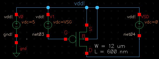
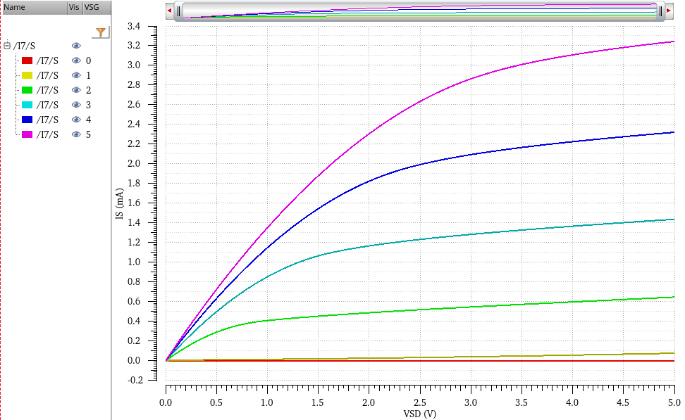
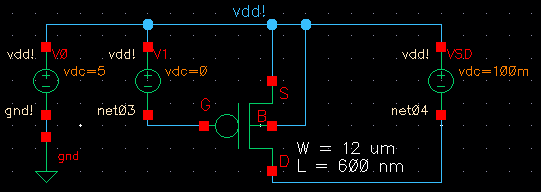
Simulation 3: I_D vs. V_SD of a PMOS.
V_SG will be tested from 0 to 5V in steps of 1V
V_SD will be tested from 0 to 5V in steps of 1mV
Here is the schematic.
Here is the simulation plot. I labelled the current I_S instead of I_D because that
is the node I used to plot it, and it looks nicer because the values are positive.
I_D would have the same magnitude, but the values would be negative as the sim
would measure it in the opposite direction.
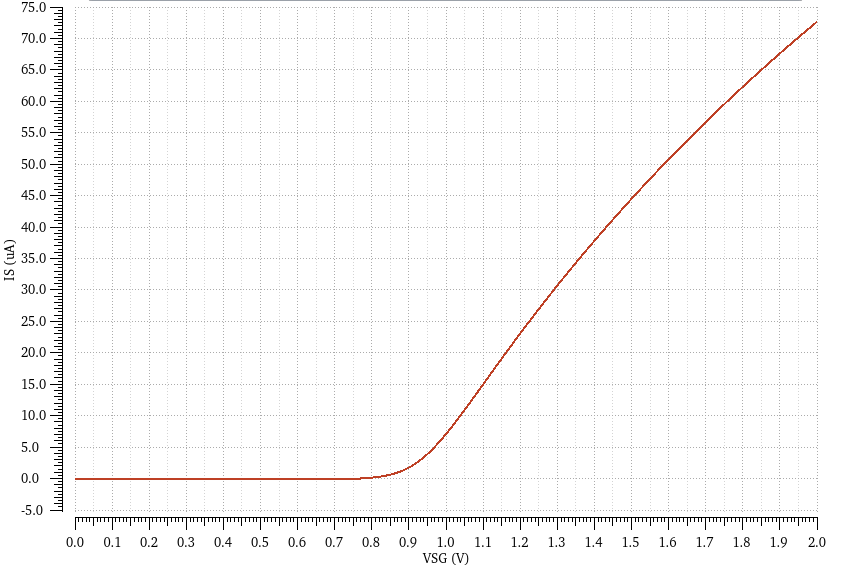
Simulation 4: I_D vs. V_SG of a PMOS. This is the same as simulation 3,
but V_SD will be kept constant at 100mV while V_SG is swept from 0 to 2V,
in steps of 1mV. Here is the schematic I used.
Here is the resulting curve, plotted as I_S against V_SG.
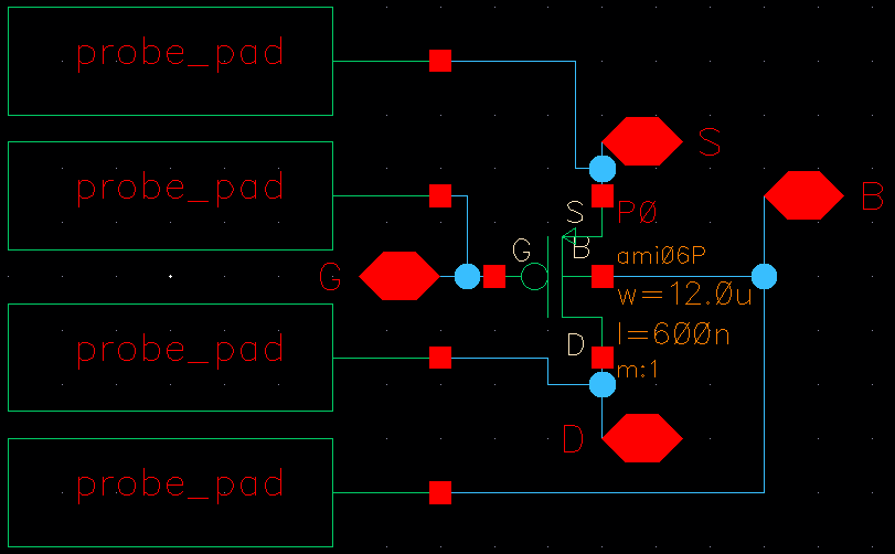
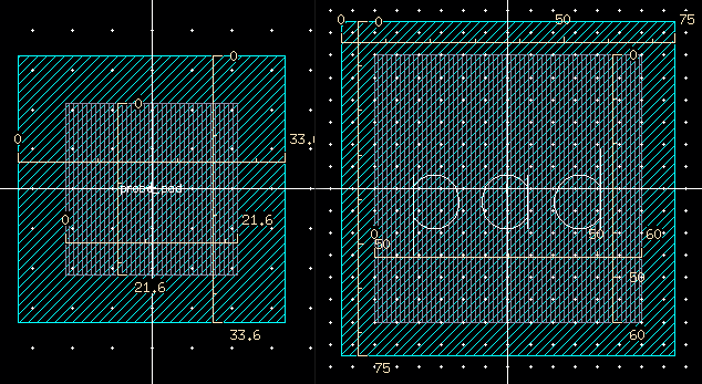
Next, we did a layout for a 6u/0.6u (W/L) NMOS with all four terminals
connected to probe pads. The cell for these probe pads was given in the
provided lab4 directory. We've used bonding pads before in the lecture
section, but these new probe pads are significantly smaller.
Here is a comparison of their relative sizes, with the probe pad on the left
and the bonding pad on the right. Aside from the size difference, they use
the same layers- metal3, (over)glass, and of course the text labels.
First, I created my NMOS schematic, with probe pads.
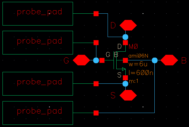
Next, I attached the probe pads to the layout I created before, also making
sure to connect the body ptap to a pin B instead of just to the gnd! net.

Here is the zoomed out version, showing the entire pads.
 Of course, I performed all the necessary verification checks.