Lab 3 - EE 421L
Prelab:
I finished the rest of Tutorial 1, which had me lay out a 1/2 voltage divider.
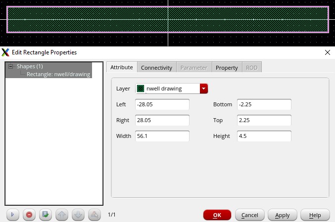
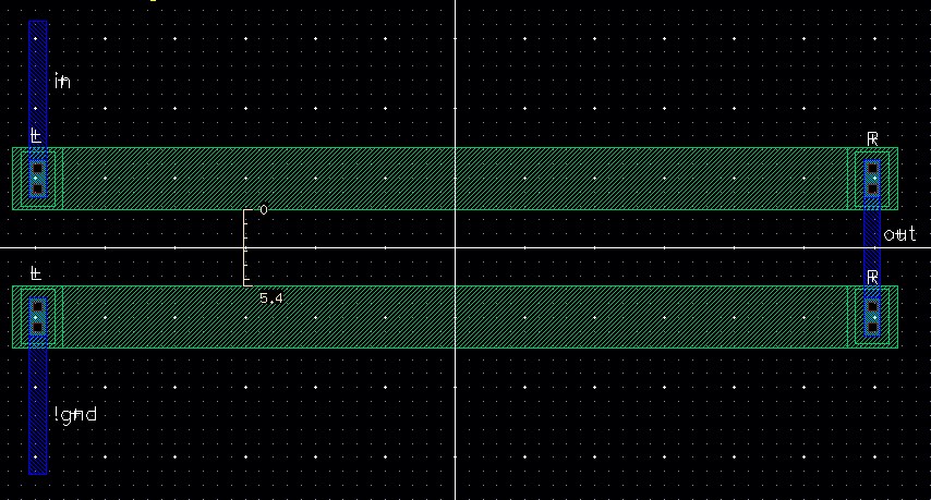
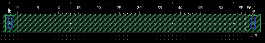
First, I made the n-well, sized 4.5um by 56.1um
Next, I added the n-taps. These provide a connection between the n-well to the Metal 1
layer on either side.
I then added L and R pins, one on each side of the resistor, allowing for connections on M1.
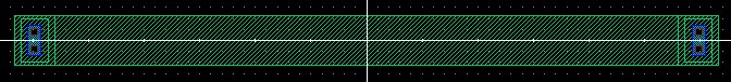
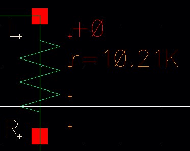
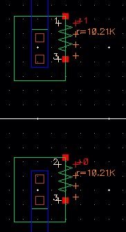
I DRC'ed the design and then extracted it, giving the following view. This specified a more
exact resistance for this element (10.21k ohms).
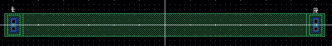
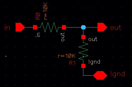
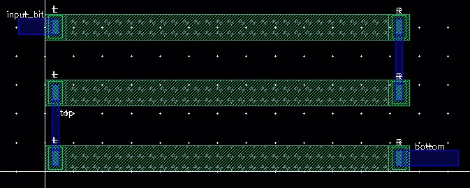
After that, I laid out the design to match the voltage divider schematic, also shown below
for clarity.
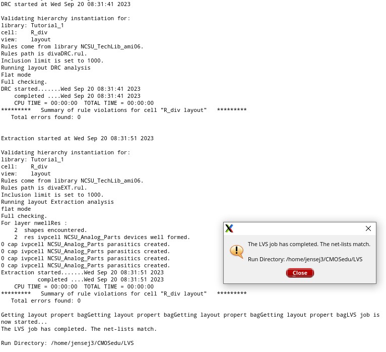
I then DRC'ed and extracted the full voltage divider layout.
Finally, here are the successful DRC, Extraction, and LVS outputs for the voltage divider.
Lab:
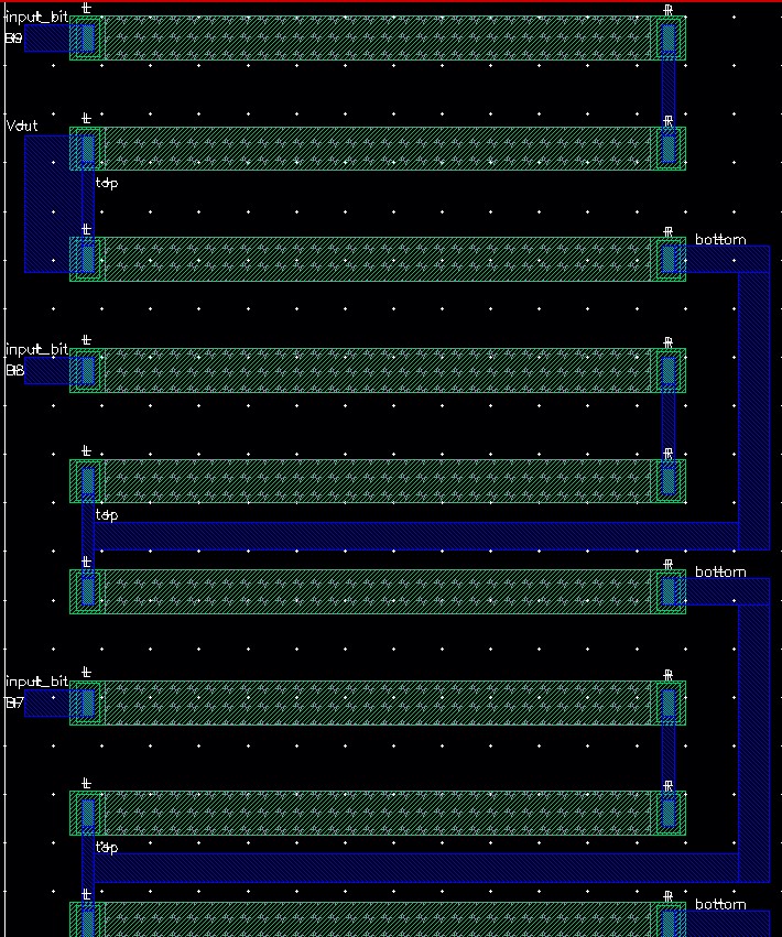
In this lab, I did the layout for my 10-bit DAC schematic from Lab 2.
This DAC design used many resistors, and these were implemented using n-wells.
N-wells have a resistance between each end, which can be calculated using this equation:
R_nwell = R_sheet * Number_squares = R_sheet * Length / Width
Since I wanted resistors of about 10k ohms, using our n-well sheet resistance of 855
(this value is obtained from the ON Semi datasheet on the C5 process we are using),
I calculated that our L/W should be 10k/855, or about 12 squares.
It will be convenient to use the same width as the 2-row ntaps I used in Tutorial 1,
so with W = 4.5um, L would be 12*4.5um = 52.63um.
However, since I already made a resistor of about 10k ohms in Tutorial 1, and knowing
that the exact value of each resistor doesn't matter too much in this design so long as
all the resistors are the same, I decided to save time and use the Tutorial 1 resistor.
The 10.21k ohm to 10k ohm difference is small enough to not matter when compared to
the slight defects that one might see in the actual manufacturing of the chip. And, because
all of the resistors are the same, the ratio will be preserved because any skew in actual
resistance values should be consistent for each n-well of the same size.
We are measuring the n-well dimensions with the length being the path between the resistor nodes,
and width being the other side of the rectangle. These are measured in micrometers (um),
and we can confirm our measurements by using the built-in ruler (keybind k).
Since I implemented my Lab 2 schematic as a modular setup connecting ten 1-bit DAC cells,
I first did the layout for one cell.
Next, I used a mosaic pattern to easily space the ten cells, and then I added another resistor
at the bottom to match my schematic. Since all of our pins had to be on the Metal 1 layer, I
decided to not use any other metal layers and instead ran M1 lines back across from the "top"
node of one cell to the "bottom" of the next cell up.
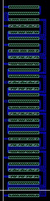
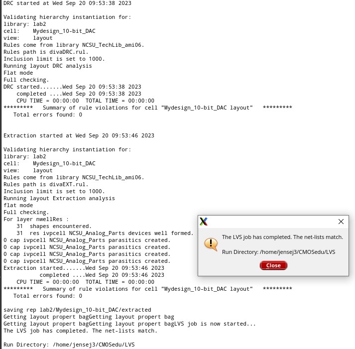
I made sure all of my pins were connected properly (notably I accidentally assigned my ground
pin as !gnd instead of gnd!, so my LVS initially failed), I performed the DRC, Extraction, and LVS
tests to ensure that my design matched my work from Lab 2.
Submission directories:
prelab: tutorial_1_submission.zip
lab: lab2_submission.zip
- The directory was originally called lab2 because I just used the same design directory from Lab 2.