Lab 2 - EE 421L
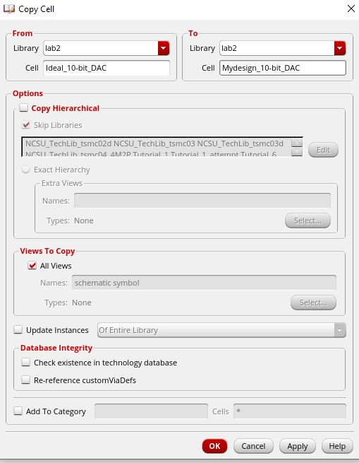
To do this, I first copied the cellview from the ideal 10-bit DAC and give it a new name.
Then I deleted the extra pins that I won't be using in my design.
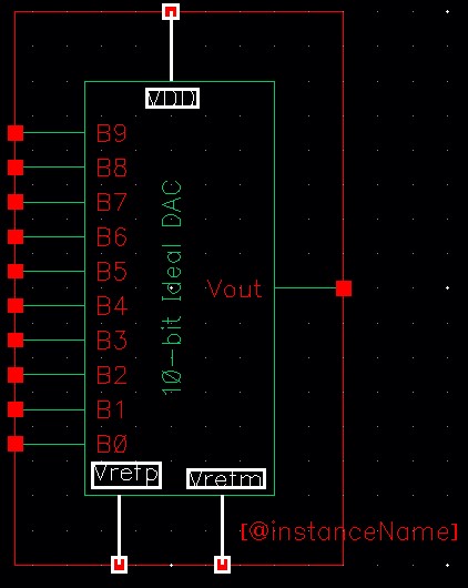
Then I renamed the symbol view to my design name.
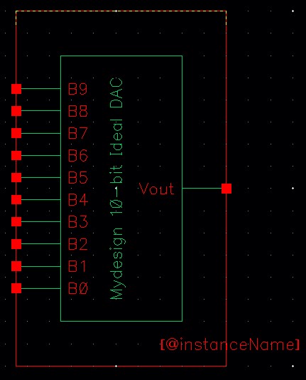
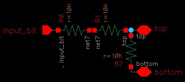
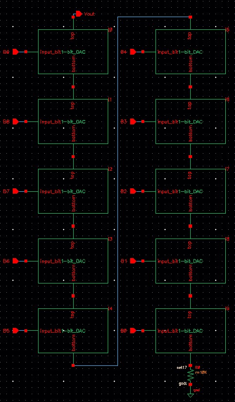
Finally, I made the 10-bit DAC schematic. The B9 to B0 pins are the digital inputs, and Vout is the analog output.
Now that I had my 10-bit DAC completed, I could make a simulation schematic to confirm it worked correctly under a load.
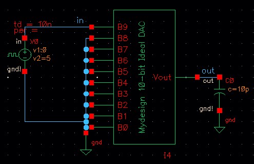
Here, I set a load of 10pF, which I expect to give a delay of about 70ns, because 0.7*R*C = 0.7 * 10k ohms * 10 pF = 70 ns.
In this simulation, since the input from B9 is 5V (mimicking a VDD of 5V and a logic high for B9), I expect that Vout will come up to 2.5V, since that is half of VDD (Vout = VDD/2^(N-n) = 5V / 2^(10-9) = 5V / 2 = 2.5V, where N = the total number of bits = 10 and n is the position of the bit being set to 1). Since our calculated time delay is for when the output reaches 50% of the expected value, I've put a marker to show the position of 2.5V/2 = 1.25V.
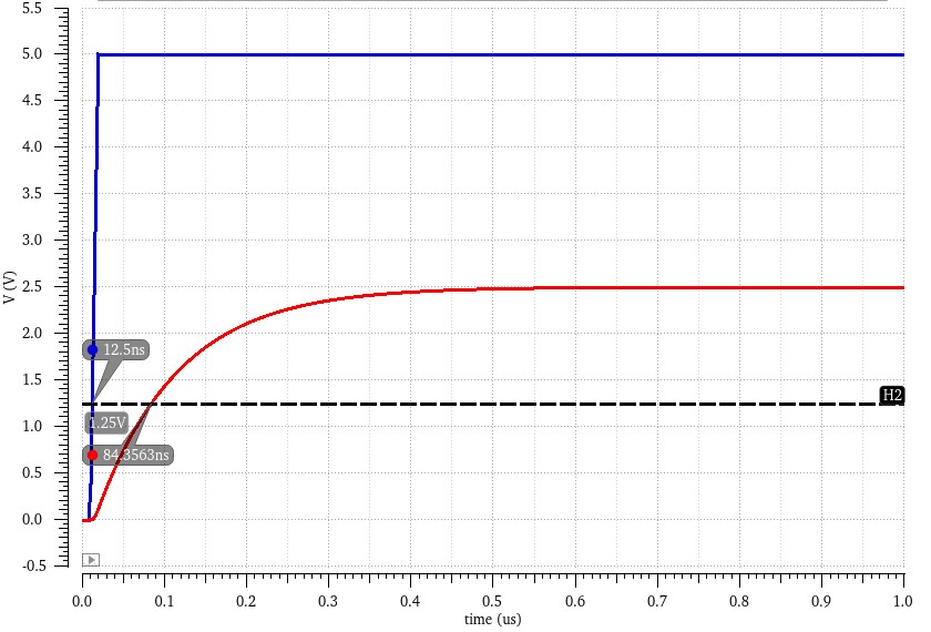
As we can see, the input reaches 1.25V at 12.5ns, and the output reaches 1.25V at 84.3563ns. This shows a time delay of a little less than 72ns, which is reasonably close to our calculated time delay for this configuration.
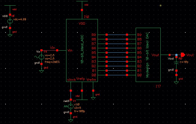
At this point, I turned back to the ADC-DAC configuration to continue testing my DAC schematic. As before, I copied the cellview for the prelab ADC-DAC simulation and just changed the DAC unit being used to the one I created. However, for the simulation to converge and have a DC solution, the VDD supply voltage needed to be 4.99V instead of 5V.
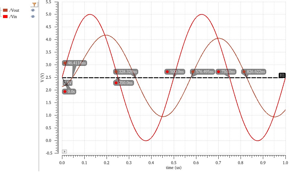
First, a simulation with no additional load being driven from the DAC:
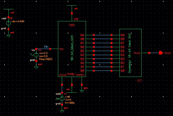
And results:
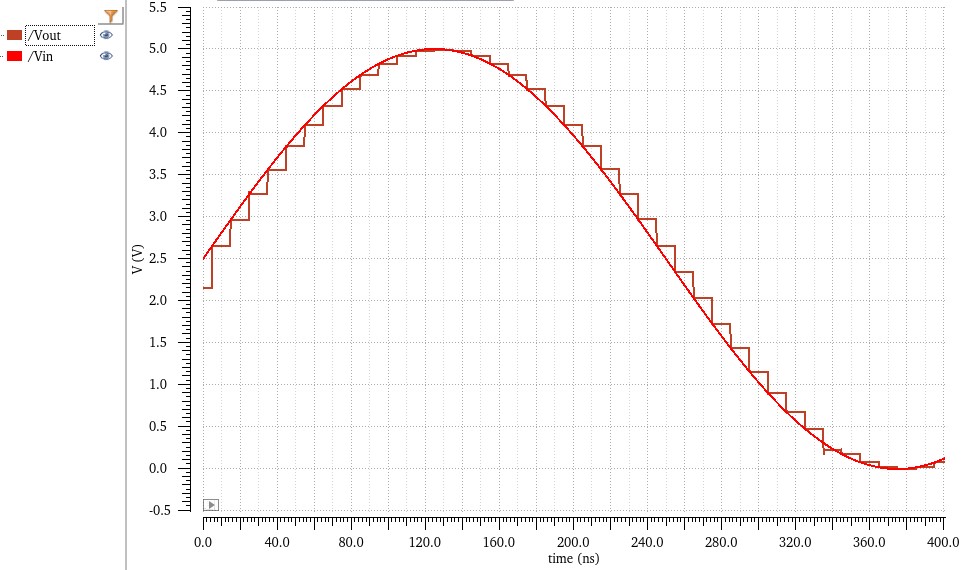
This was the same result as the prelab, confirming that my design works correctly.
Next, a simulation with the DAC driving an additional 10k-ohm resistor load:
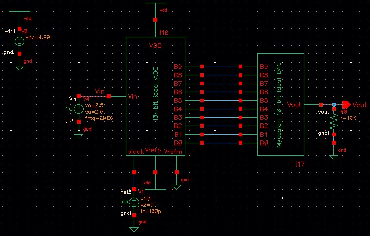
And results:
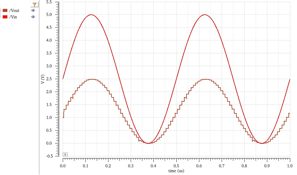
Here we effectively see a voltage divider, since the output resistance of the DAC is 10k ohms and this is placed in series with the 10k ohm load. The output voltage is in phase with the input, but only ranges from 0-2.5V instead of from 0-5V.
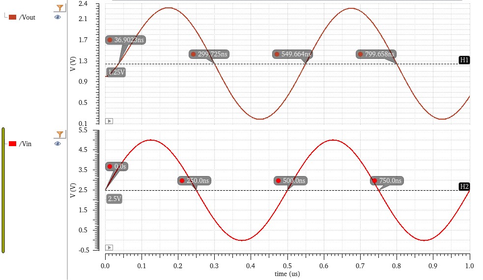
A simulation with the DAC driving a 10pF capacitor load (having removed the additional 10k-ohm):
And results:
Since this is effectively an RC circuit, we see the magnitude and phase differences between the input and output that we would expect in that situation.
Finally, a simulation with the DAC driving both the additional 10k-ohm and 10pF capacitor, in parallel:
And results:
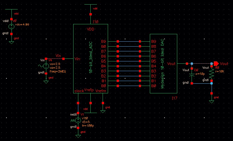
This basically just combined the prior two cases, showing the magnitude and phase change from the capacitor as well as the overall magnitude decrease from the resistor.