Input Capacitance
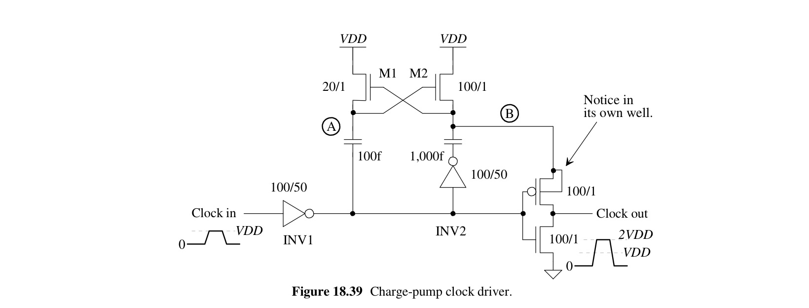
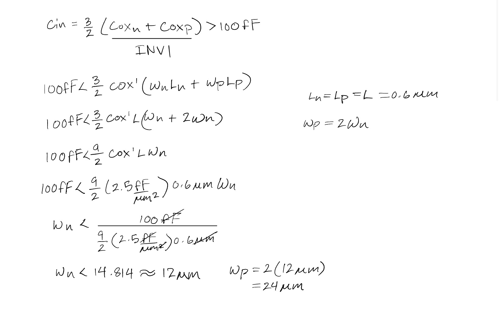
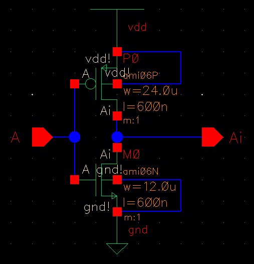
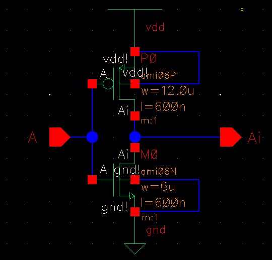
I started with the sizing of INV1. The required parameter was that the input capacitance Cin is less than 100fF. The input capacitance is only present in INV1. To achieve this I used the equation Cin = (3/2)(Coxp+Coxn). Assuming the length to be the minimum 0.6um, I was able to determine the width of the NMOS and PMOS to be 12um and 24um. The math can be seen below.
INV1 schematic
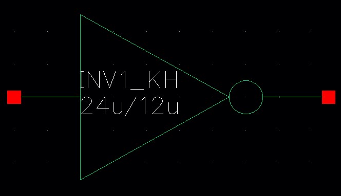
INV1 symbol
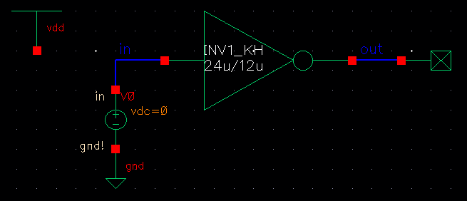
With my INV1 designed I simulated the operation of the inverter and got its switching point using a DC sweep.
INV1 simulation schematic
INV1 simulation
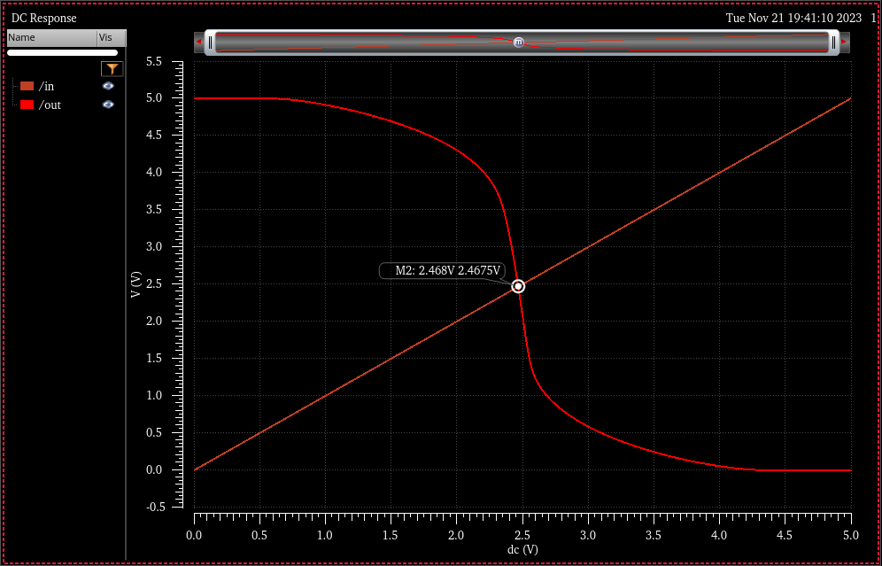
As can be seen in the simulation the switching point is at about 2.4V this falls within the parameters of logic low is 1V or less and logic high is 3V or more.
INV2
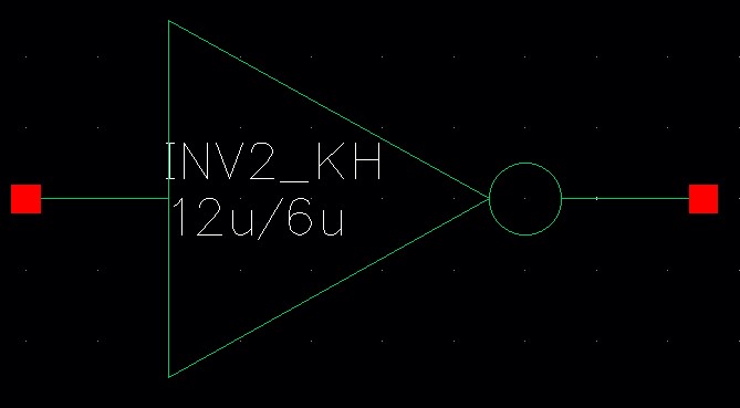
The sizing of INV2 is 12u/6u. The reason I chose this is that it will give me a switching point of 2.5V which is needed to invert the output of inverter 1 at about the half point. I made the inverter smaller to save on layout space and I don't need a large inverter for this part.
INV2 schematic
INV2 symbol
INV2 simulation schematic
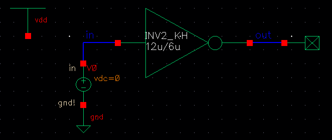
INV2 simulation schematic
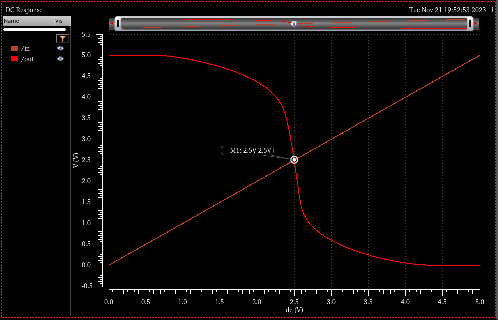
The switching point is at 2.5V proving the proper operation of this inverter.
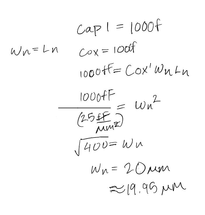
Capacitor 1
The capacitor on the left side of the circuit can be smaller due to the fact that it is not supplying power to the load of the circuit. I will be using NMOSs in strong inversion to reduce layout size. I chose to stick with the 100fF capacitance for my design ;however, I needed a bigger capcitor to turn on M2 so I chose to use 1pF. My hand calculations on sizing the MOSFET can be seen below. The reason I used W=L is to reduce the layout size of the MOSFET.
Capacitor 2
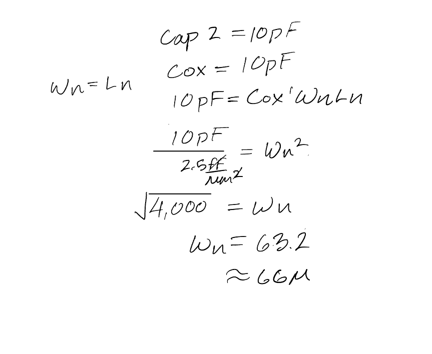
The capacitor on the right side of the circuit supplies power to the load so this capacitor must have a larger capacitance than the load. To determine the capacitance needed I used the equation for charge sharing between capacitors.
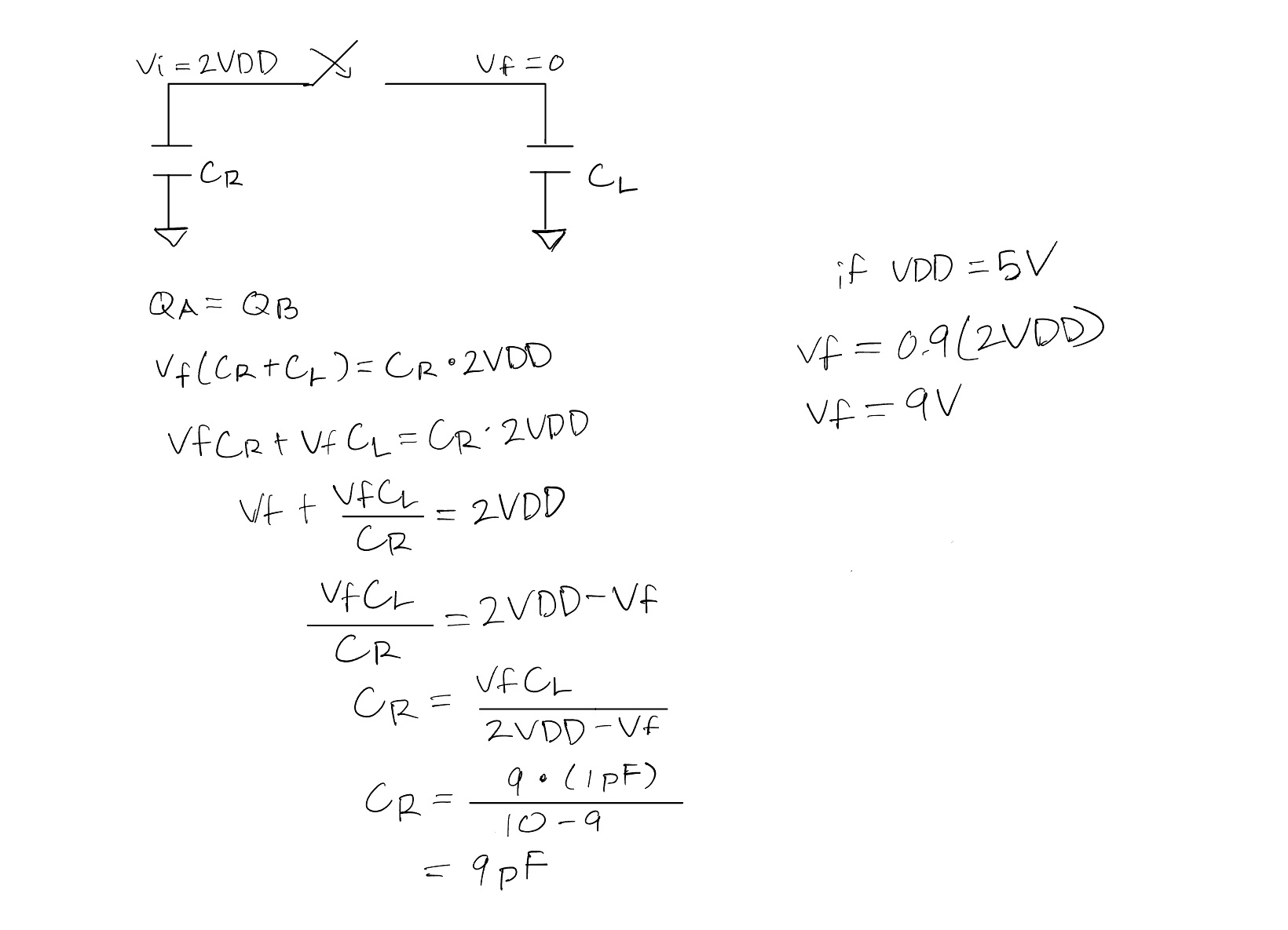
I determined that I would need a 9pF capacitor to supply power to the load at VDD. I increased the needed capacitance to 10pF load to ensure that the capacitor is able to drive the 1pF load. For the size of the NMOS needed I used the hand calculations below.
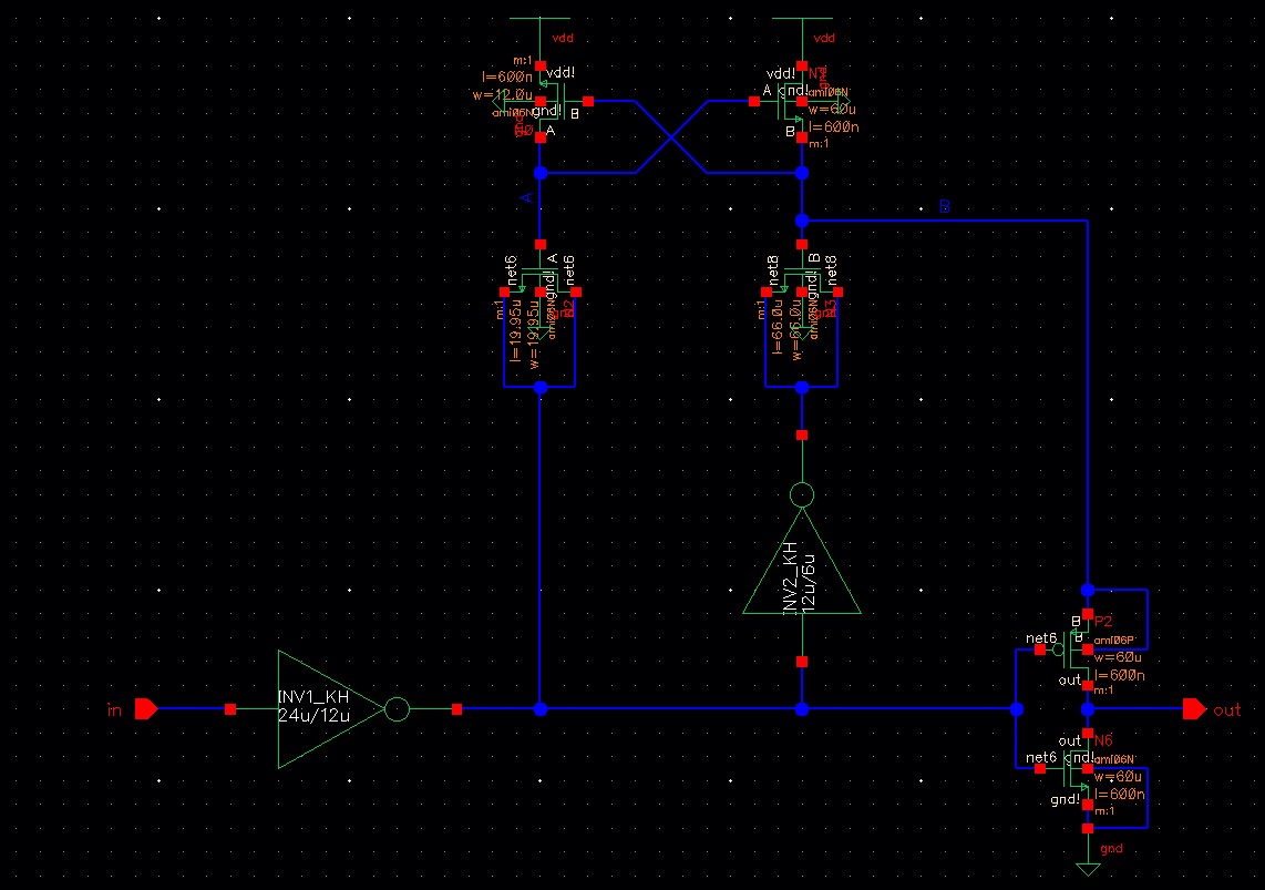
M1 and M2
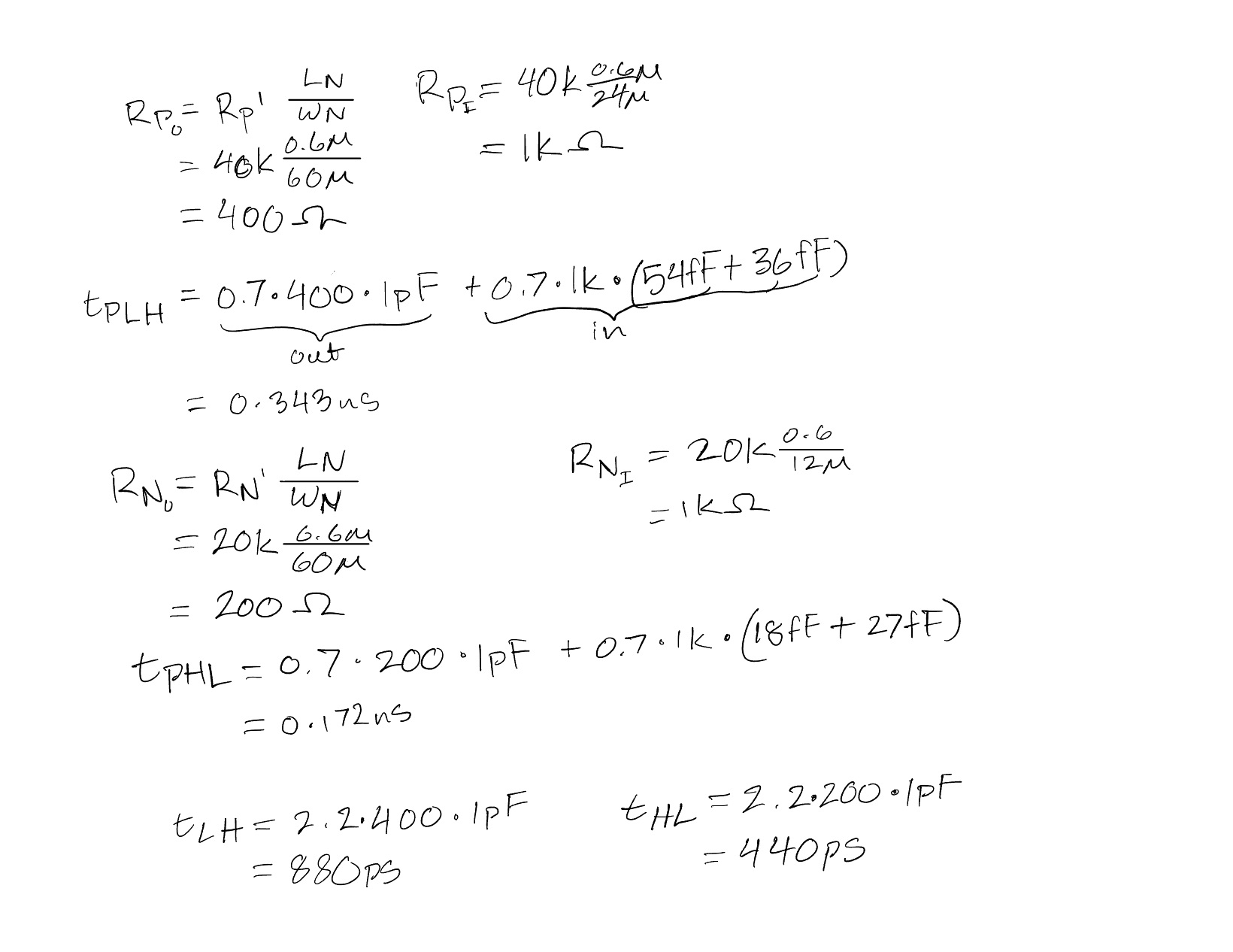
For the MOSFETs at the top of the circuit M1 charges capacitor 1 to VDD and M2 charges capacitor 2 to VDD. Capacitor 1 is small so the sizing of M1 can be smaller to reduce layout size and power. The opposite is true for M2. It must be larger to charge capacitor 2 faster. If these MOSFETs are sized to small the capacitors will not be able to charge fast enough with changing input pulses. For this reason I used the MOSFET ratios in the figure to get the sizes M1=12u/0.6u and M2=60u/0.6u.
Output Inverter
For this inverter I chose to use the ratios in the figure. Assuming 0.6um for the length of the MOSFETs so for the width of the MOSFETs I used 60um. The reason I made these bigger is to drive a higher current to the load.
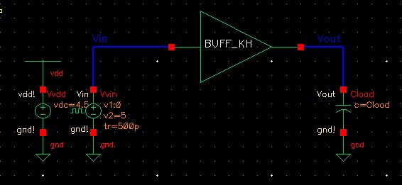
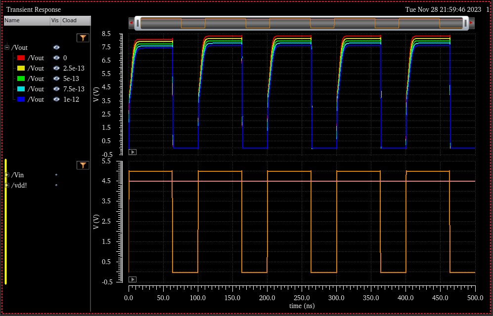
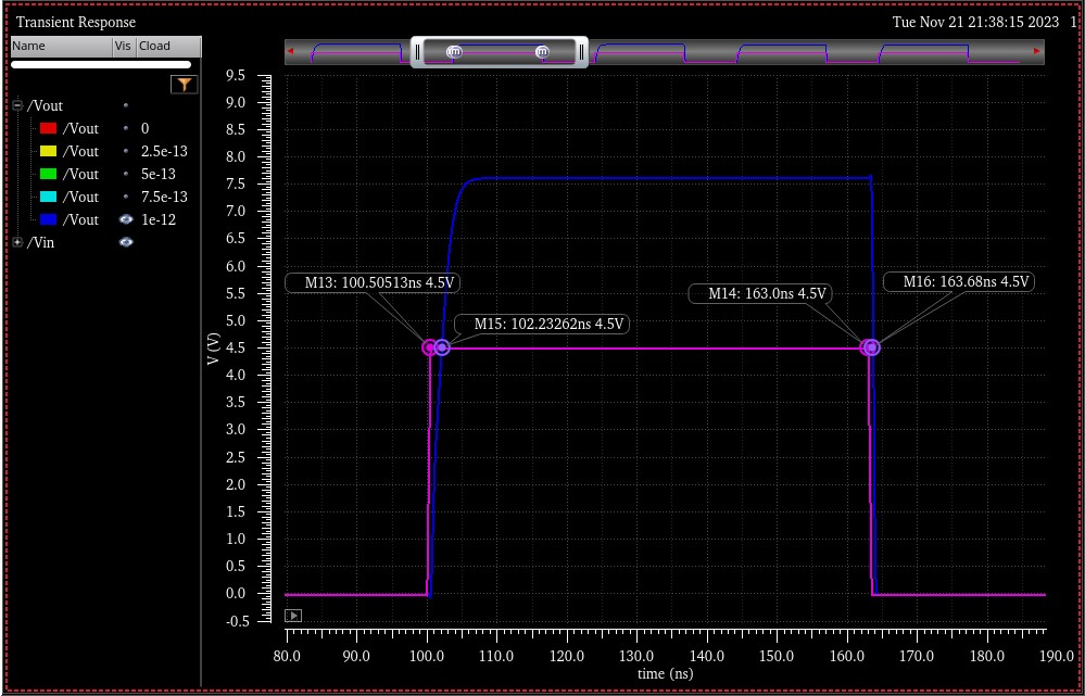
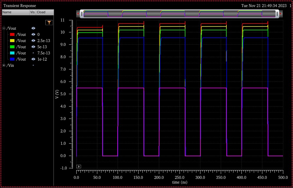
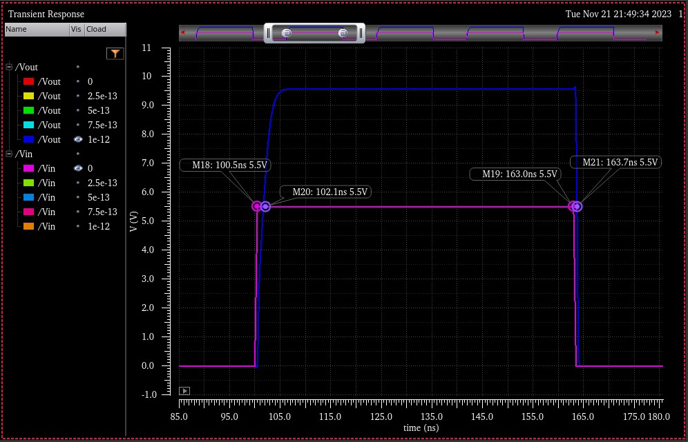
Final Buffer Schematic and Simulations
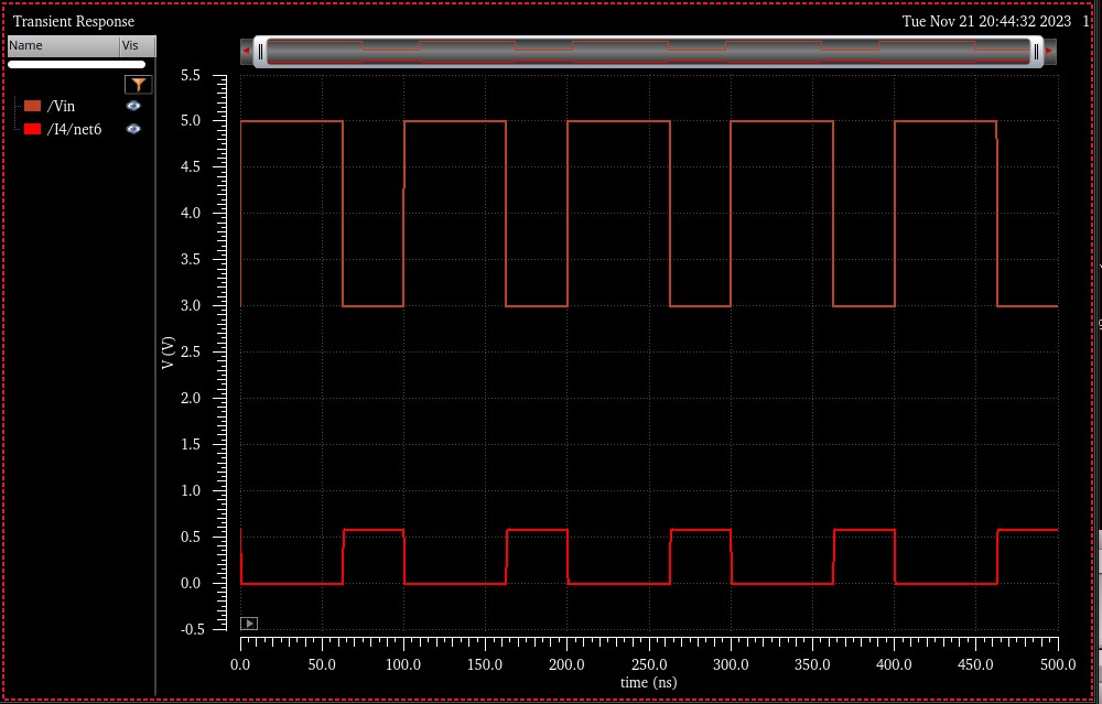
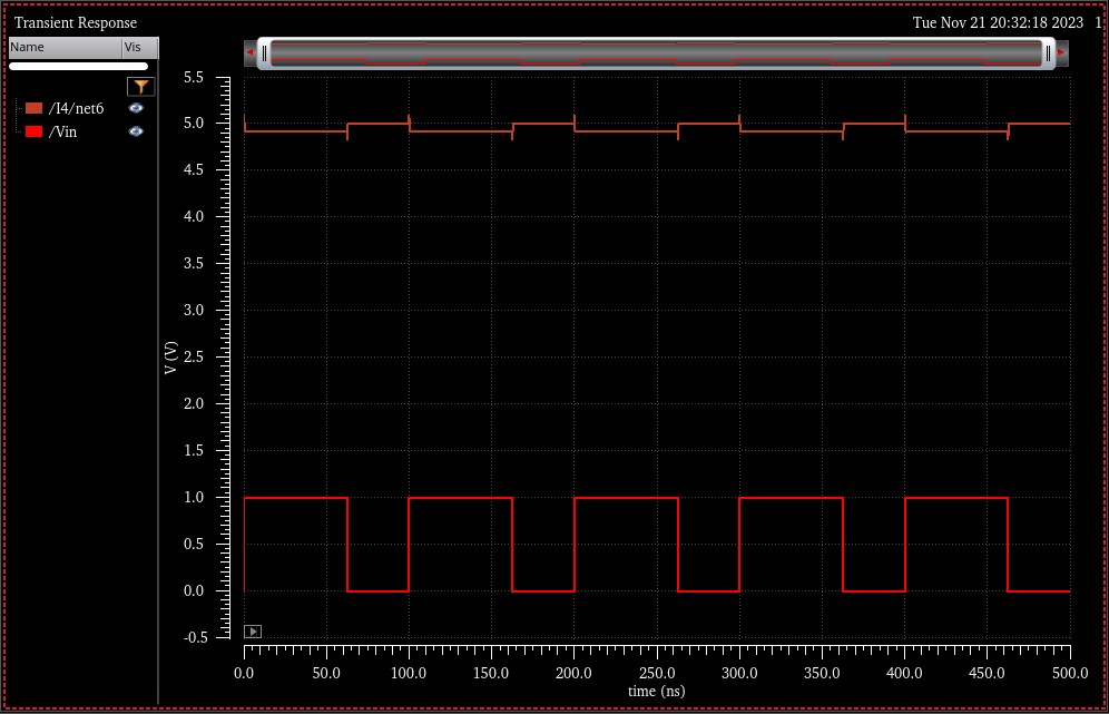
Putting all these pieces together I made the circuit below and simulated it to make sure it was operating correctly and within parameters.
Buffer Schematic