Lab 7 - ECE 421L
Authored
by Kanoa Hokoana, hokoana@unlv.nevada.edu
October 25, 2023
Lab 7: Using buses and arrays in the design of word inverters, muxes, and high-speed adders
For the prelab I went through tutorial 5.
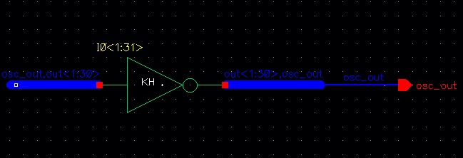
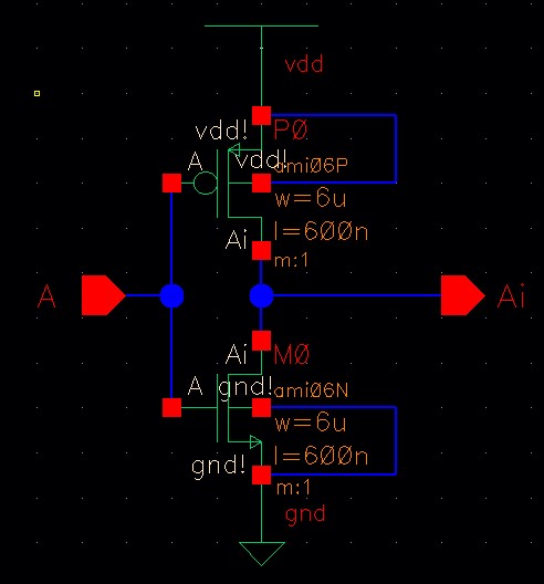
For tutorial 5 I made a ring oscillator. This is the schematic for the ring oscillator.
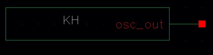
I then made a symbol.
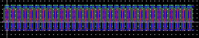
Then I made a layout for the ring oscillator.
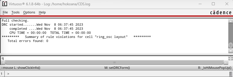
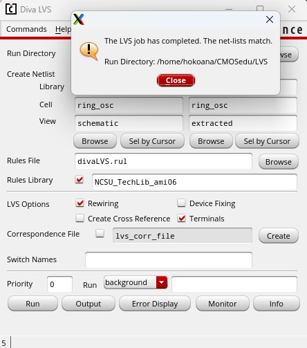
DRC and LVS check
This concludes tutorial 5 and the prelab.
For the first part of the lab I created a 4-bit inverter. I then created an 8-bit NAND, NOR, AND, inverter, and OR gate.
After
that I drafted an 8-bit DEMUX/MUX. Finally, I drafted an 8-bit
full-adder. All drafted logic units used 6u/0.6u NMOS and PMOS devices.
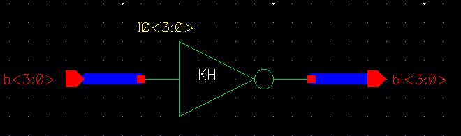
4-bit inverter
1-bit inverter schematic
4-bit inverter schematic
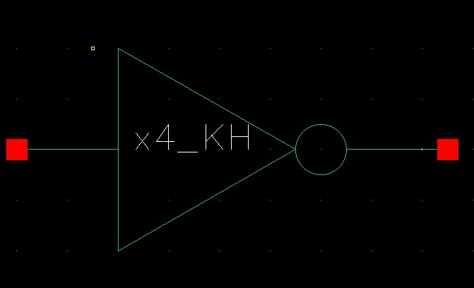
4-bit inverter symbol
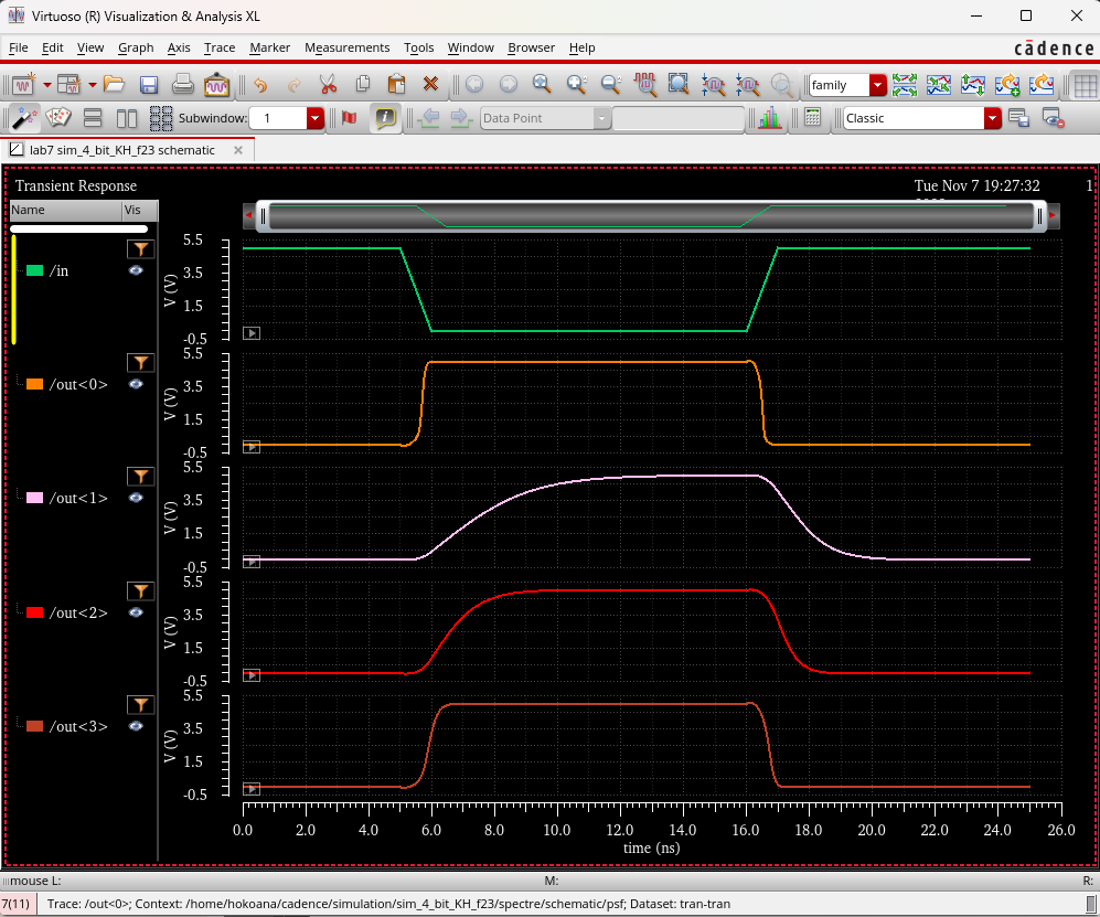
4-bit inverter simulation schematic
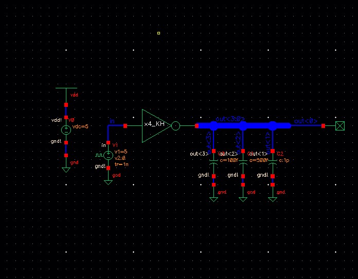
Simulation
8-bit inverter
Schematic
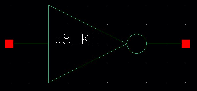
Symbol
8-bit NAND Gate
1-bit NAND Gate schematic
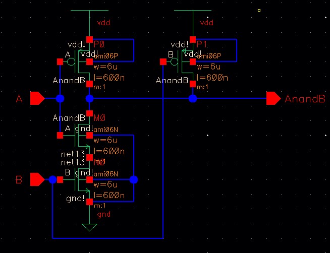
8-bit NAND Gate schematic
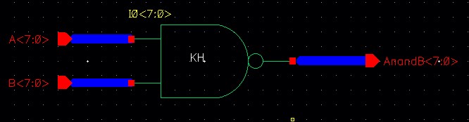
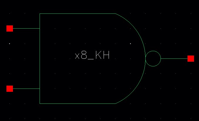
8-bit NAND Gate symbol
8-bit NOR Gate
1-bit NOR Gate schematic
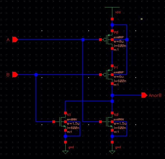
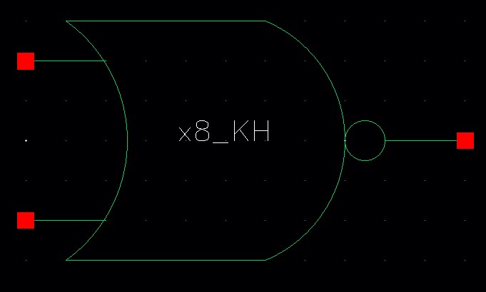
8-bit NOR Gate schematic
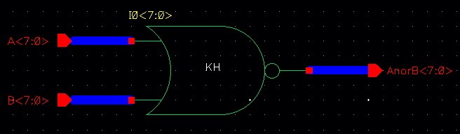
8-bit NOR Gate symbol
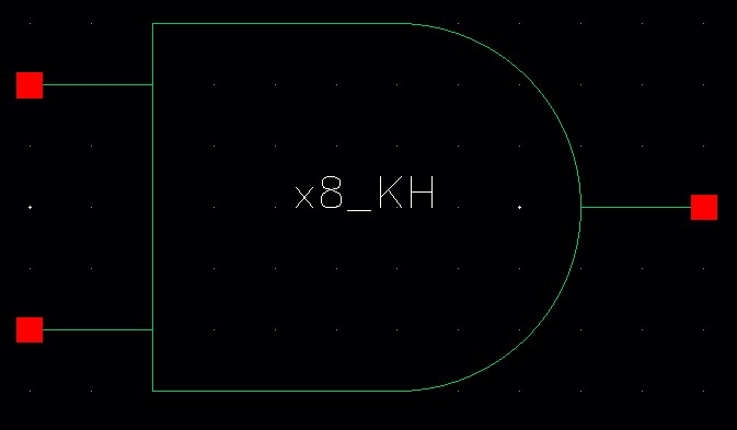
8-bit AND Gate
Schematic
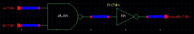
Symbol
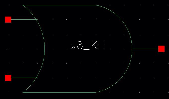
8-bit OR Gate
Schematic
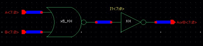
Symbol
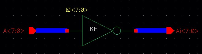
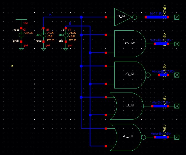
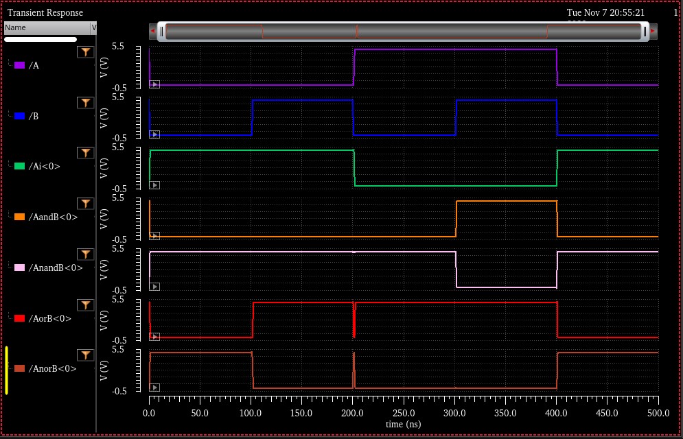
Simulation of NAND, NOR, AND, Inverter, and OR gates
Simulation Schematic
Simulation
2 to 1 DEMUX/MUX
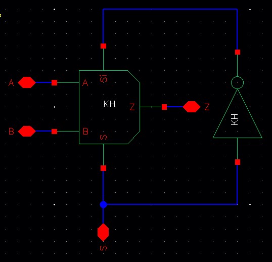
1-bit Schematic
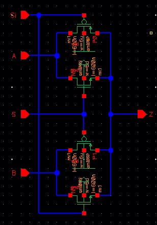
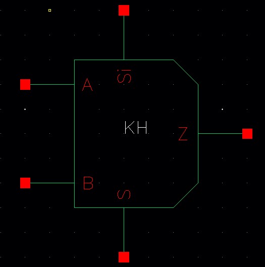
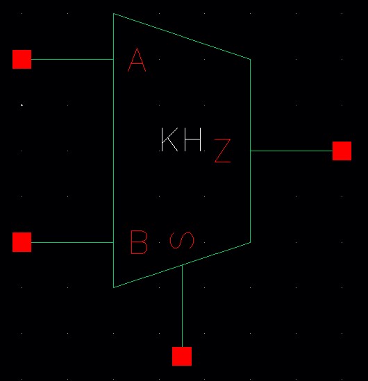
1-bit symbol
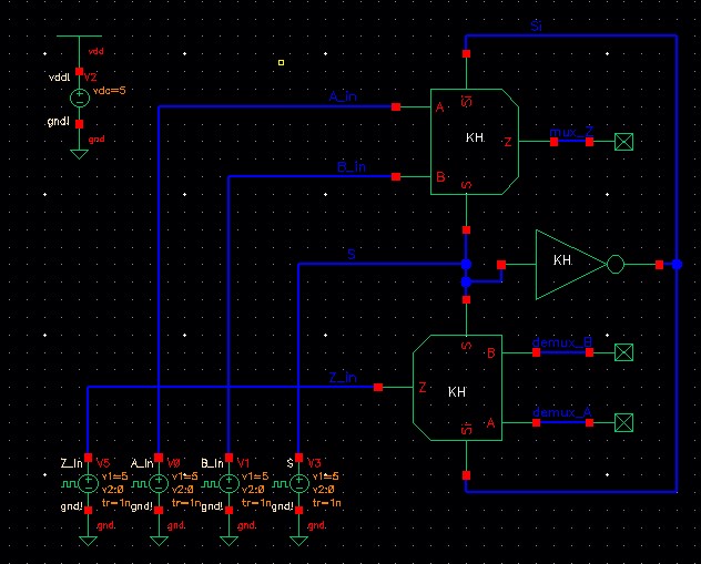
1-bit Simulation Schematic
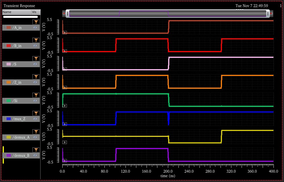
1-bit Simulation
A
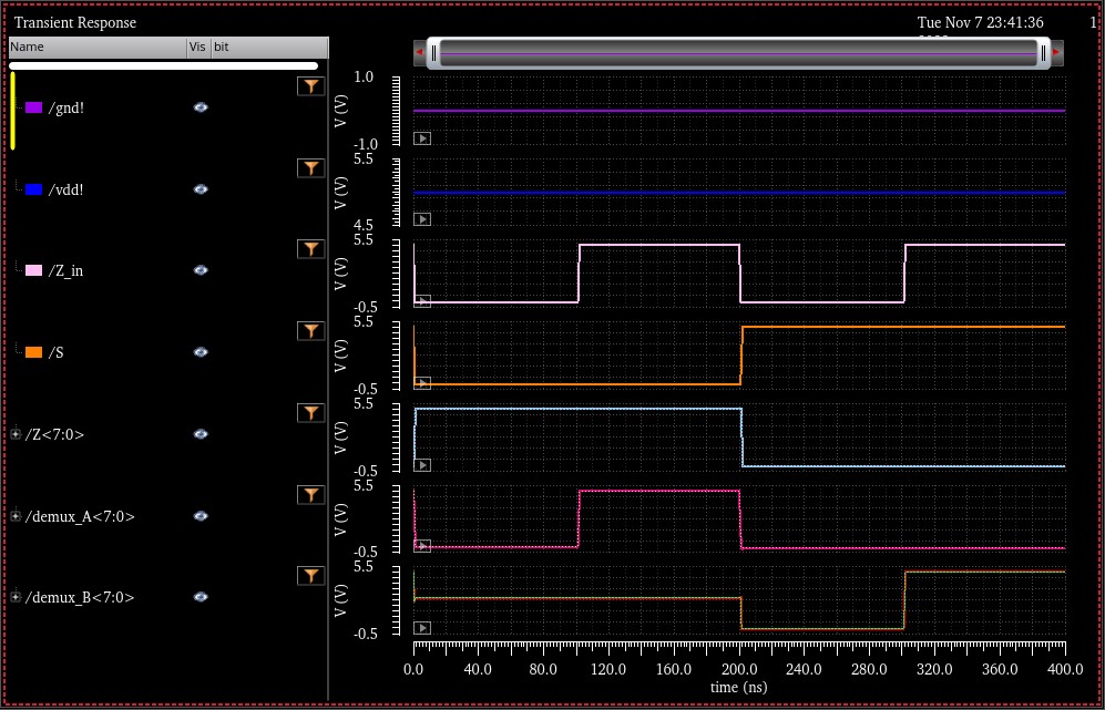
MUX chooses which input signal will be outputted when S is "1" A is
outputted to Z and when Si is "1" B is outputted to Z. A DEMUX does the
opposite when S is "1" the input Z is outputted to A and when Si is "1"
the input Z is outputted to B.
8-bit DEMUX/MUX
1-bit Schematic
1-bit Symbol
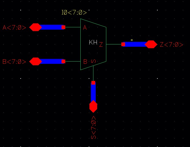
8-bit Schematic
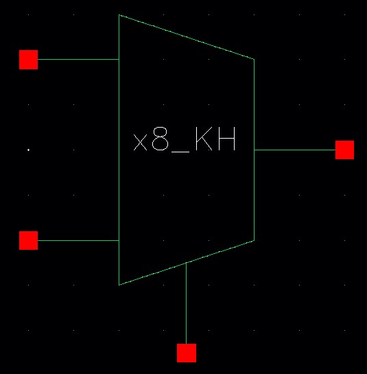
8-bit Symbol
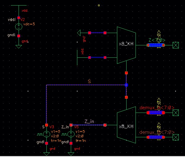
8-bit Simulation Schematic
8-bit Simulation
8-bit Full-adder
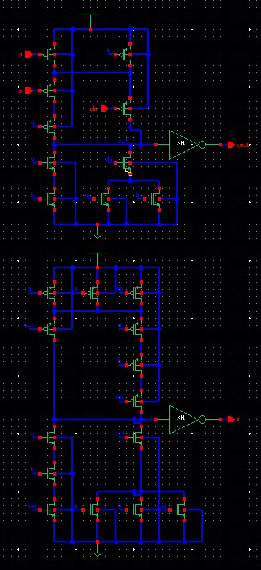
1-bit Schematic
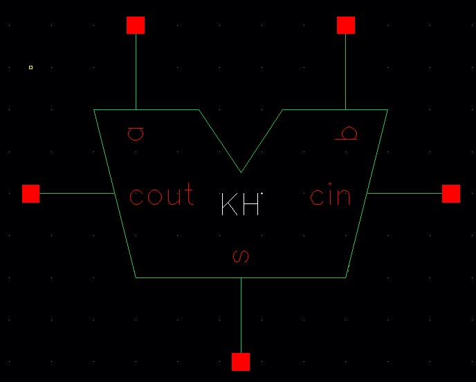
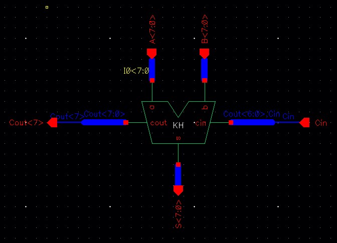
1-bit Symbol
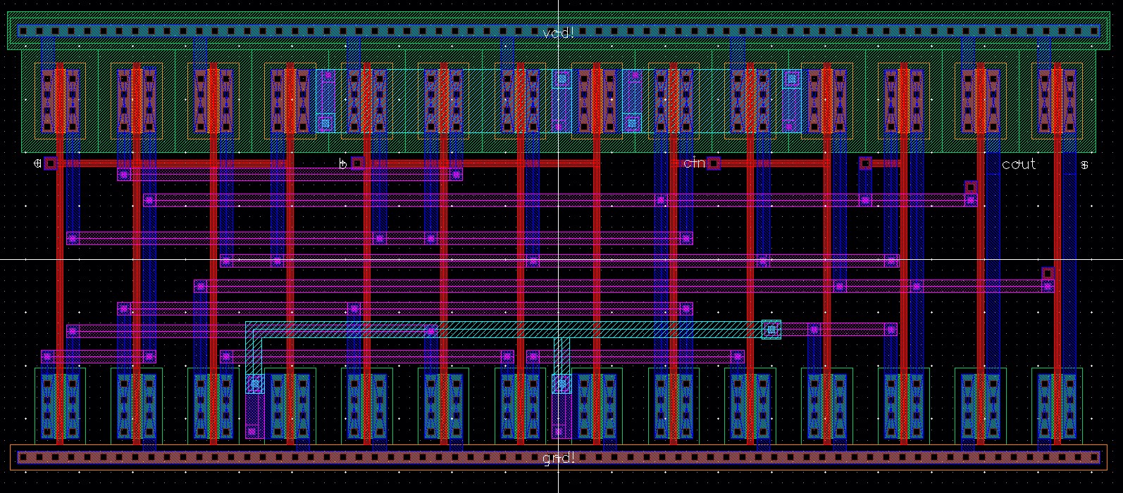
1-bit Layout
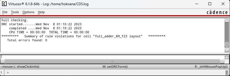
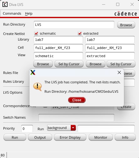
1-bit DRC and LVS Check
8-bit Schematic
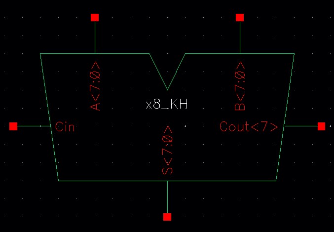
8-bit Symbol
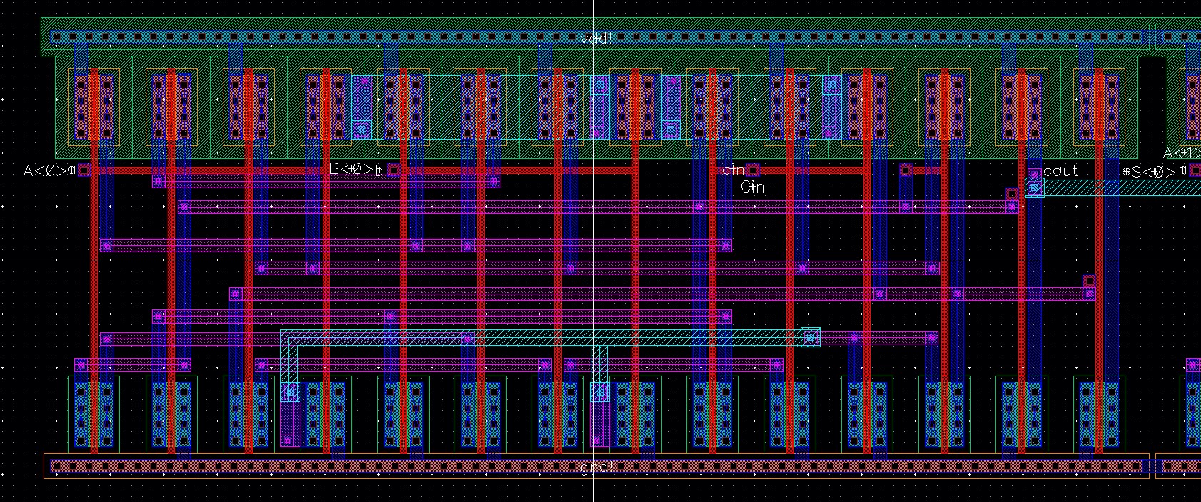
8-bit Layout

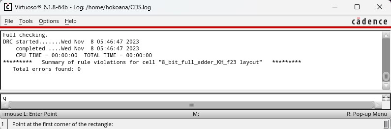
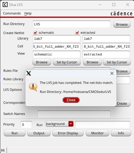
8-bit DRC and LVS Check
8-bit Simulation Schematic
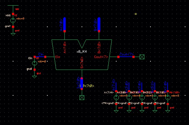
8-bit Simulation
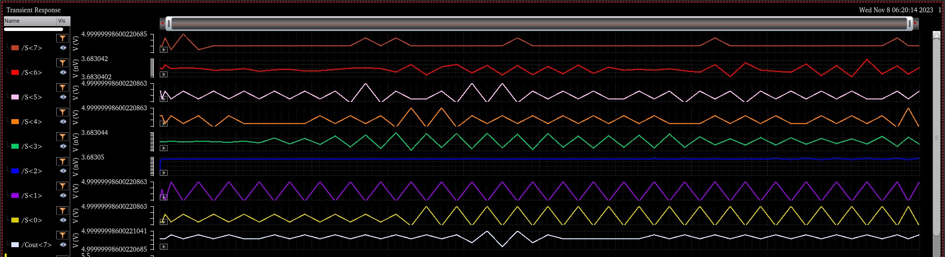
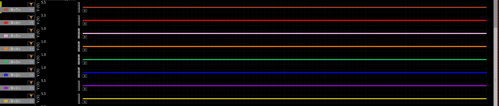
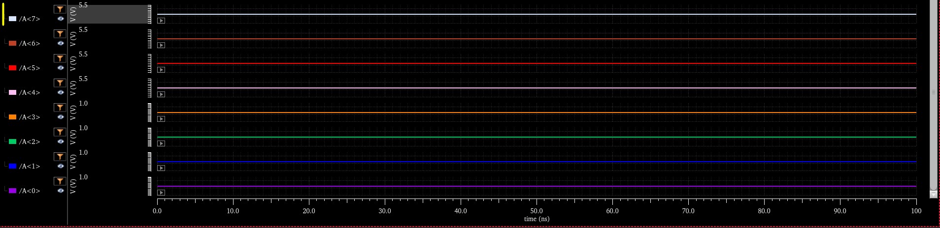
I
used the two binary numbers A = 11110000 and B = 11000011. The result
is Cout = 1 and S = 10110011. This can be seen in the simulation above.
This concludes lab 7.Backing up work
These are the files used in this lab: lab7.zip
This completes lab 7.
Return to EE 421L Labs