Lab 6 - ECE 421L

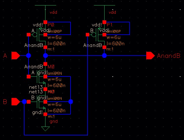
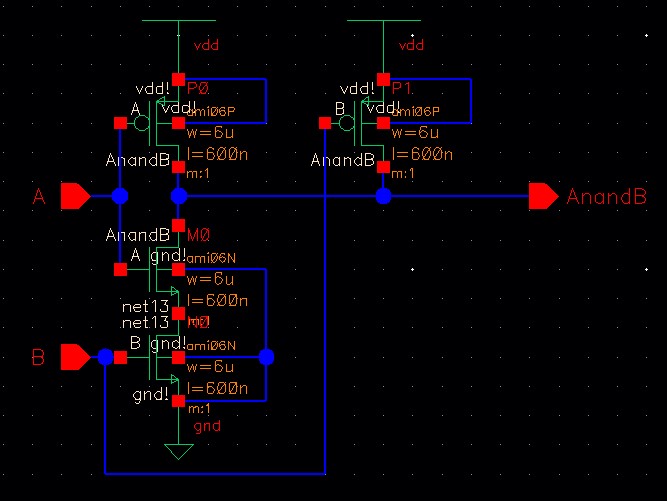
This is the schematic for the 2-input NAND gate.
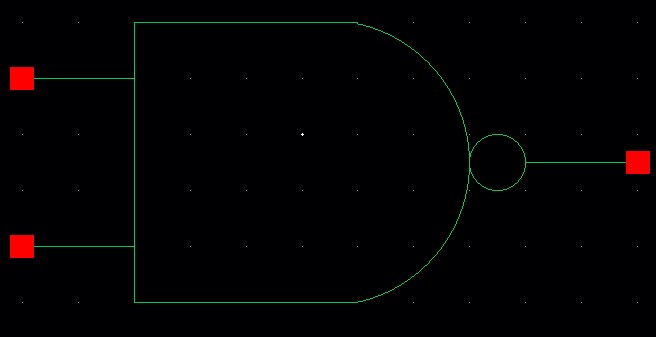
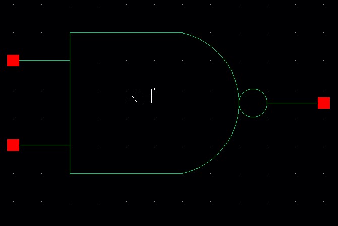
I then made the symbol for the schematic.
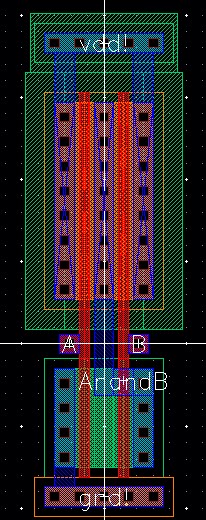
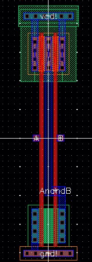
Then I made the layout for the 2-input NAND gate.
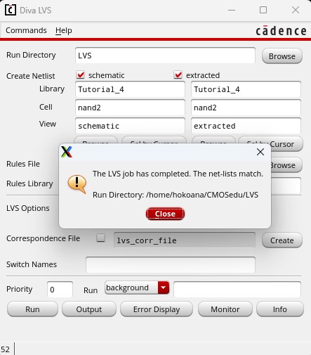
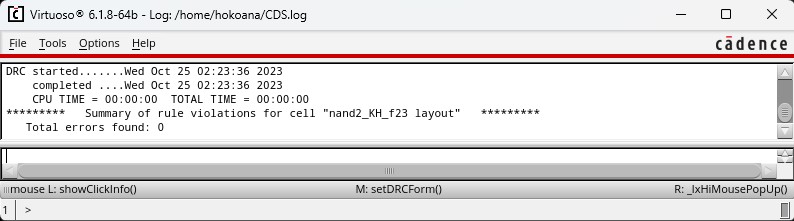
DRC and LVS Check
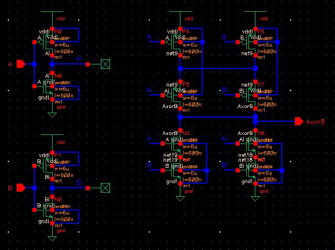
I then drafted the schematic for the 2-input XOR gate.
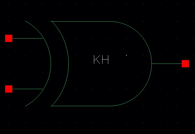
I then created a symbol for the 2-input XOR gate.
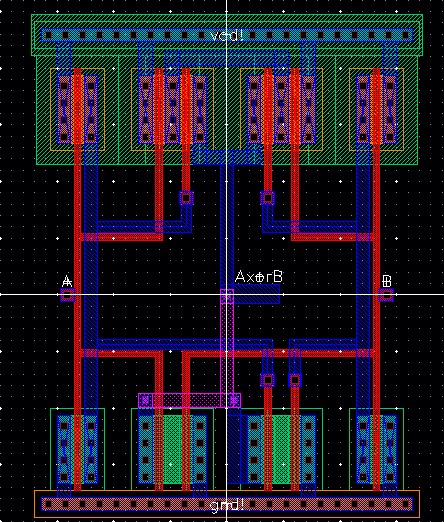
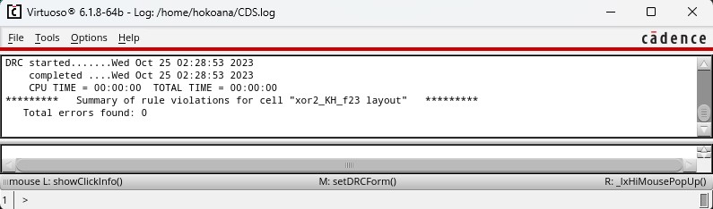
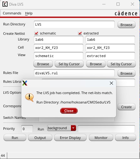
I then drafted the layout for the 2-input XOR gate.
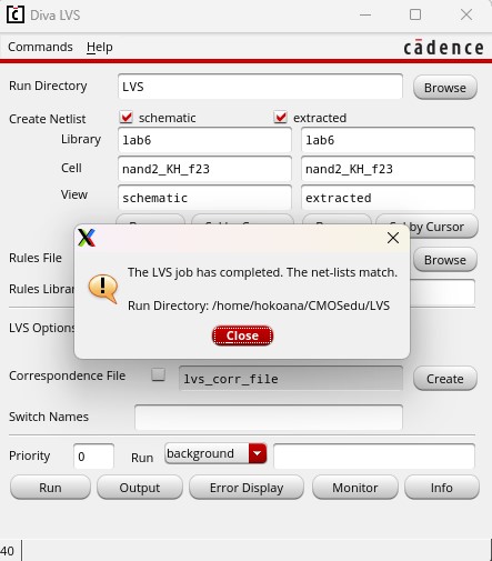
DRC and LVS Check
I then simulated the gates for all possible inputs using the schematic below
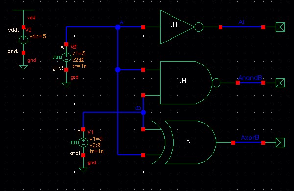
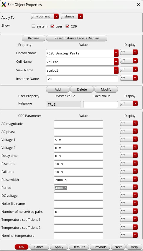
I set up the vpulse to simulate a digital input.
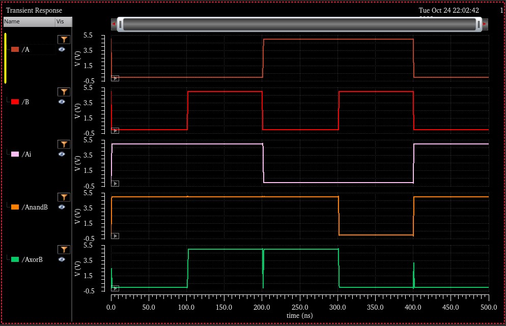
As seen above the outputs and inputs match with the truth tables below.
NAND Gate
| A | B | AnandB | |
| 0 | 0 | 1 | |
| 0 | 1 | 1 | |
| 1 | 0 | 1 | |
| 1 | 1 | 0 |
XOR Gate
| A | B | AxorB | |
| 0 | 0 | 0 | |
| 0 | 1 | 1 | |
| 1 | 0 | 1 | |
| 1 | 1 | 0 |
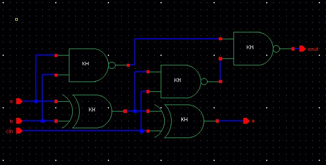
I then drafted the schematic for a full-adder.
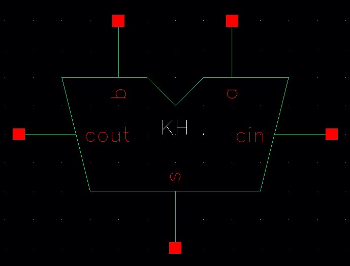
I then made a symbol for the full-adder.
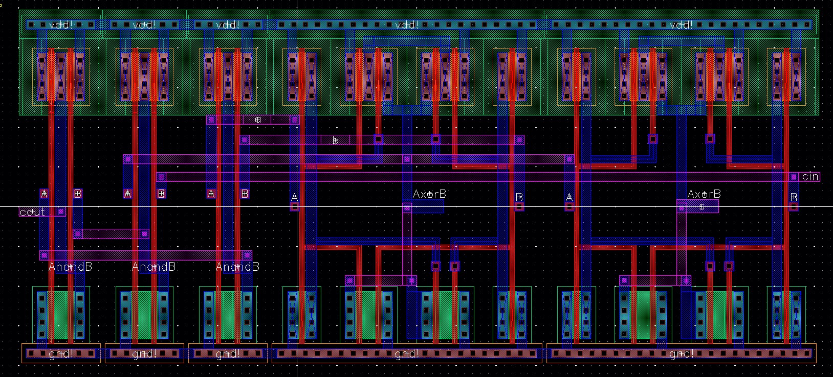
I then drafted the layout for a full-adder.
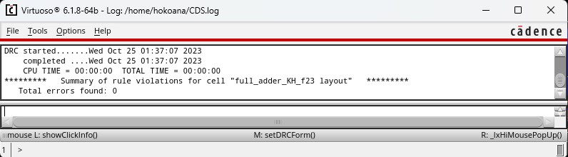
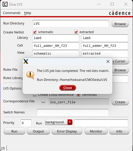
DRC and LVS check
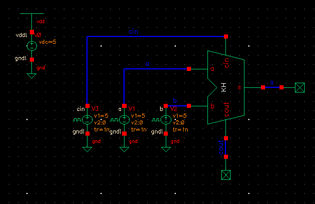
I then simulated the full-adder for all possible inputs using the schematic below.
This is the simulation
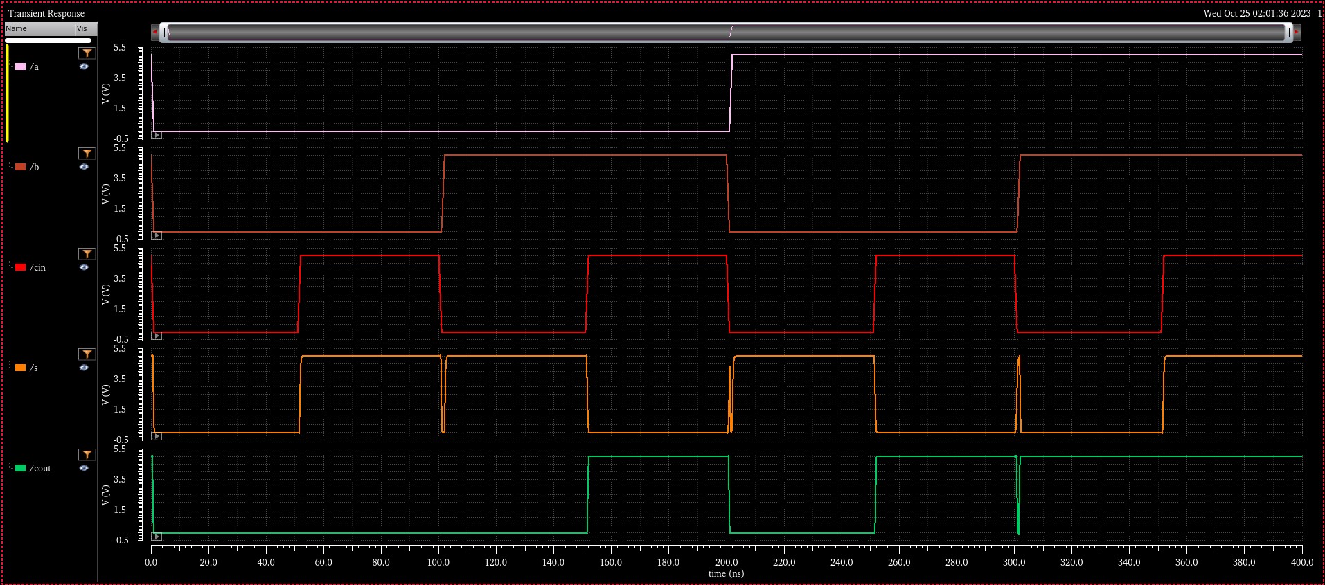
The simulation matches the output of the full-adder truth table below.
Full-Adder
| a | b | cin | s | cout | |
| 0 | 0 | 0 | 0 | 0 | |
| 0 | 0 | 1 | 1 | 0 | |
| 0 | 1 | 0 | 1 | 0 | |
| 0 | 1 | 1 | 0 | 1 | |
| 1 | 0 | 0 | 1 | 0 | |
| 1 | 0 | 1 | 0 | 1 | |
| 1 | 1 | 0 | 0 | 1 | |
| 1 | 1 | 1 | 1 | 1 |
Backing up work

These are the files used in this lab: lab6.zip
This completes lab 6.