Lab 5 - ECE 421L
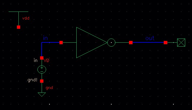
I then made another schematic with the symbol.
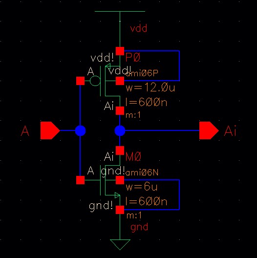
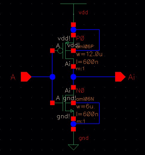
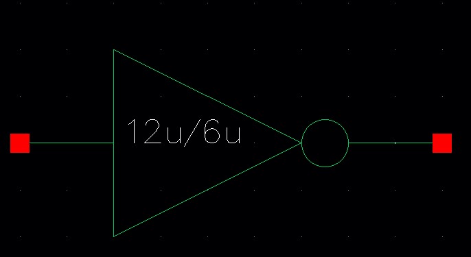
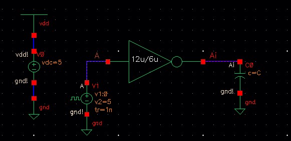
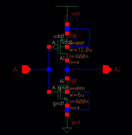
This is the schematic for the 12u/6u inverter.
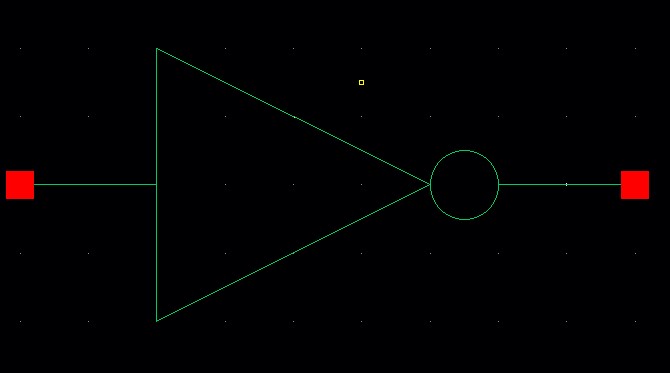
I then made the symbol for the schematic.
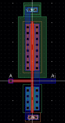
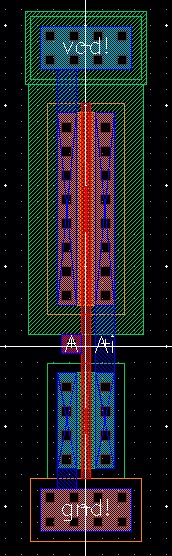
Then I made the layout for the 12u/6u inverter.
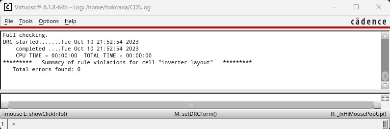
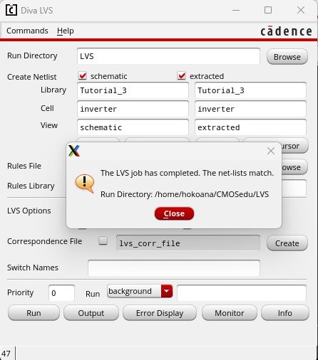
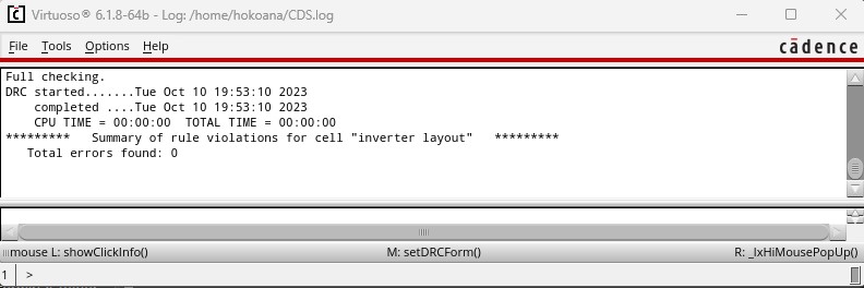
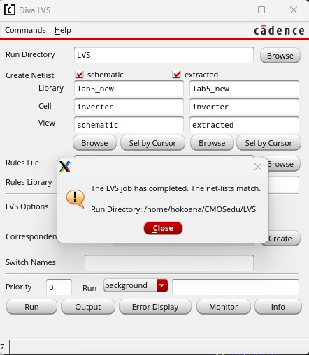
DRC and LVS Check
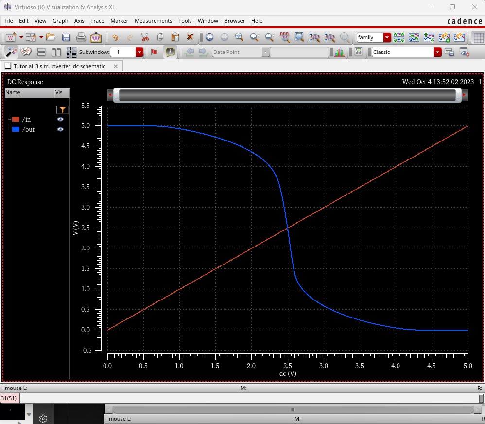
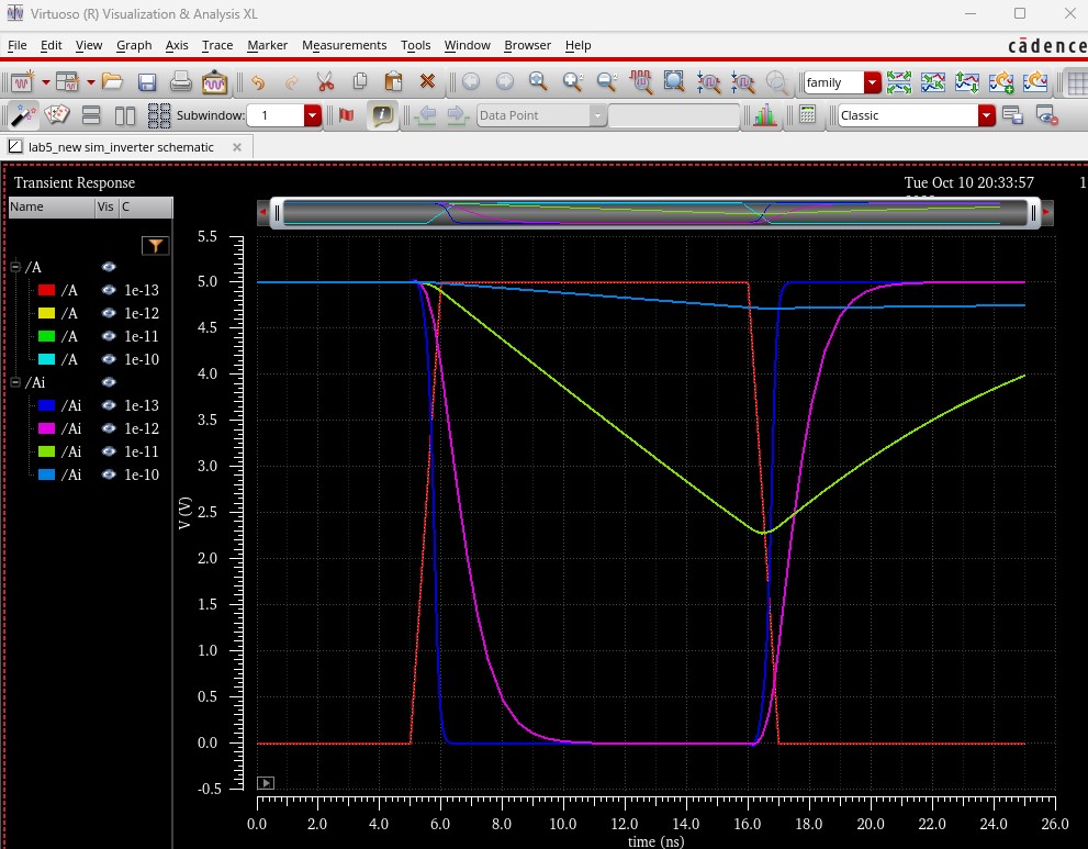
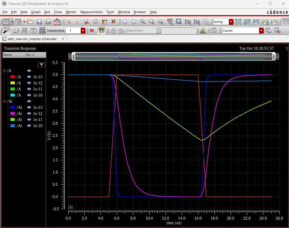
I then simulated the 12u/6u inverter driving a 100 fF, 1 pF, 10 pF, and 100 pF capacitive load.
Spectre
Ultrasim
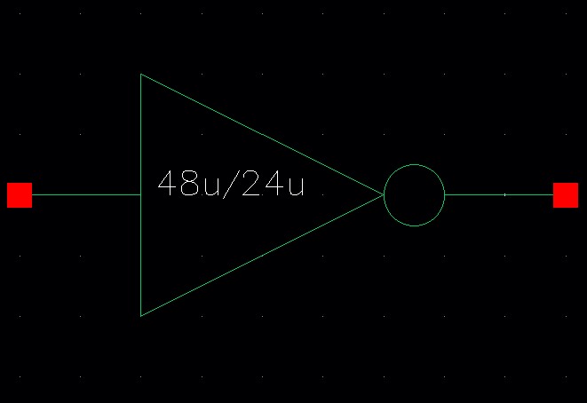
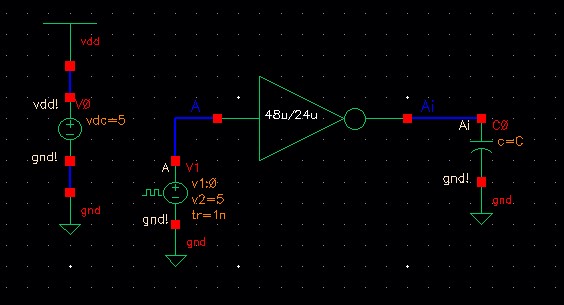
I then drafted the schematic for 48u/24u inverter.
I then created a symbol for the 48u/24u inverter.
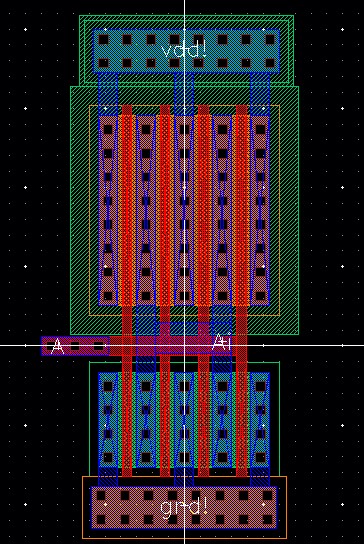
I then drafted the layout for the 48u/24u inverter.
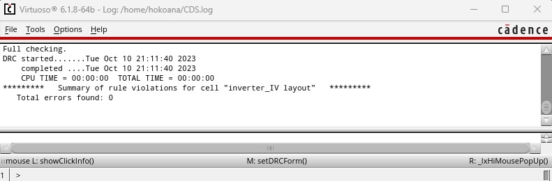
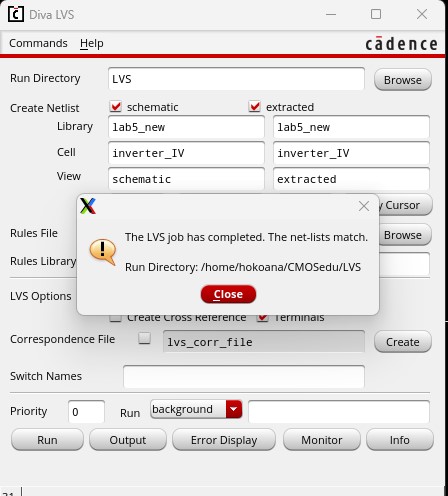
DRC and LVS Check
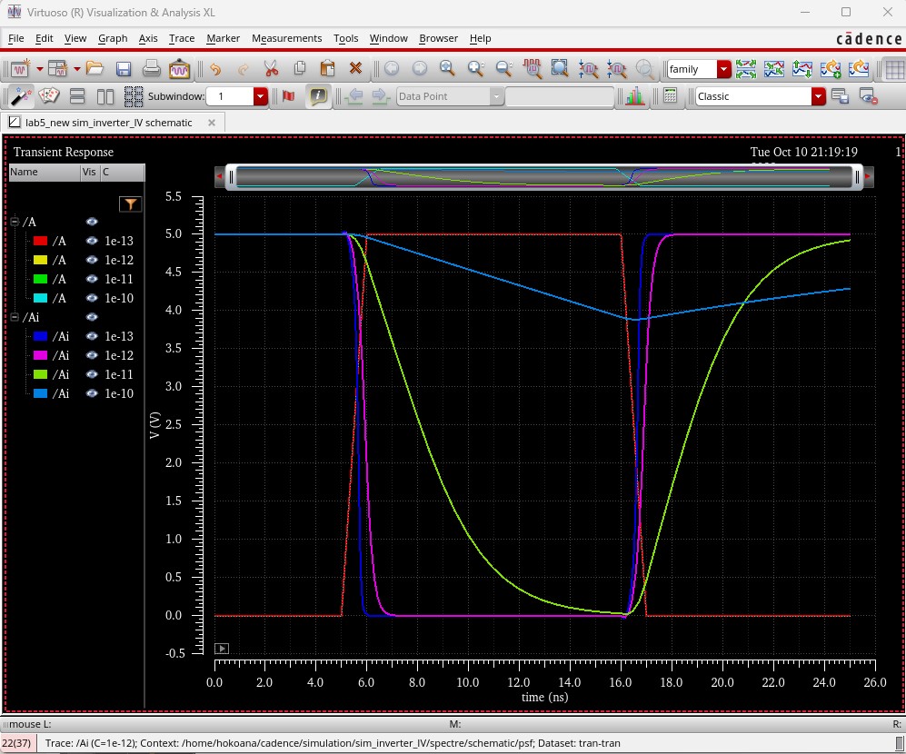
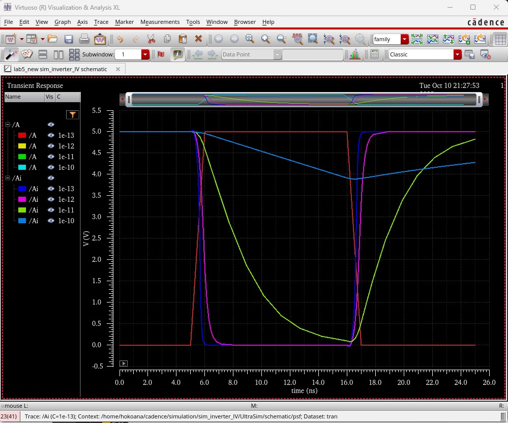
I then simulated the 48u/24u inverter driving a 100 fF, 1 pF, 10 pF, and 100 pF capacitive load.
Spectre
Ultrasim
These are the files used in this lab: lab5_new.zip
Backing up my work
This completes lab 5.